

Page 1
www.iButton.com
SPECIAL FEATURES
Real-Time Clock/calendar in binary format
Uses the same binary time/date representation
as the DS1994 but with 1 second resolution
Clock accuracy is better than ± 2 minutes per
month at 25°C
Operating temperature range from -40°C to
+70°C
Over 10 years of operation
PRELIMINARY
DS1904
RTC iButton
Presence detector acknowledges when reader
first applies voltage
Meets UL#913 (4th Edit.); Intrinsically Safe
Apparatus, Approved under Entity Concept
for use in Class I, Division 1, Group A, B, C
and D Locations (application pending)
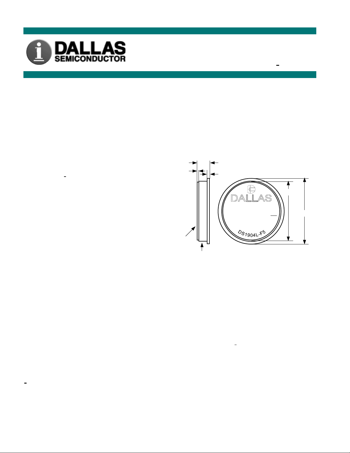
F5 MicroCan
5.89
COMMON iButton FEATURES
Unique, factory–lasered and tested 64-bit
registration number (8-bit family code + 48bit serial number + 8-bit CRC tester) assures
absolute traceability because no two parts are
alike
Multidrop controller for MicroLAN
Digital identification and information by
momentary contact
Chip-based data carrier compactly stores in-
formation
Data can be accessed while affixed to object
Economically communicates to host with a
single digital signal at 16.3k bits per second
Standard 16 mm diameter and 1-Wire proto-
col ensure compatibility with iButton Device
family
Button shape is self-aligning with cup-shaped
probes
Durable stainless steel case engraved with
registration number withstands harsh environments
Easily affixed with self-stick adhesive back-
ing, latched by its flange, or locked with a
ring pressed onto its rim
0.36 0.51
16.25
YYWW REGISTERED RR
40 24
000000FBC52B
DATA
GROUND
All dimensions are shown in millimeters
ORDERING INFORMATION
DS1904L-F5 F5 MicroCan
EXAMPLES OF ACCESSORIES
DS9096P Self-Stick Adhesive Pad
DS9101 Multi-Purpose Clip
DS9093RA Mounting Lock Ring
DS9093A Snap-In Fob
DS9092 iButton Probe
17.35
iButton DESCRIPTION
The DS1904 RTC iButton is a rugged real-time clock module that can be accessed with minimal
hardware. Data is transferred serially via the 1-Wire protocol, which requires only a single data lead and a
ground return. The DS1904 contains a unique 64-bit factory-lasered ROM and a real-time clock/calendar
implemented as a binary counter. The durable MicroCan package is highly resistant to environmental
1 of 12 022400
Page 2
DS1904
hazards such as dirt, moisture, and shock. Accessories permit the DS1904 to be mounted on almost any
surface including printed circuit boards and plastic key fobs. The DS1904 adds functions such as
calendar, time and date stamp, stopwatch, hour meter, interval timer, and logbook to any type of
electronic device or embedded application that uses a microcontroller.
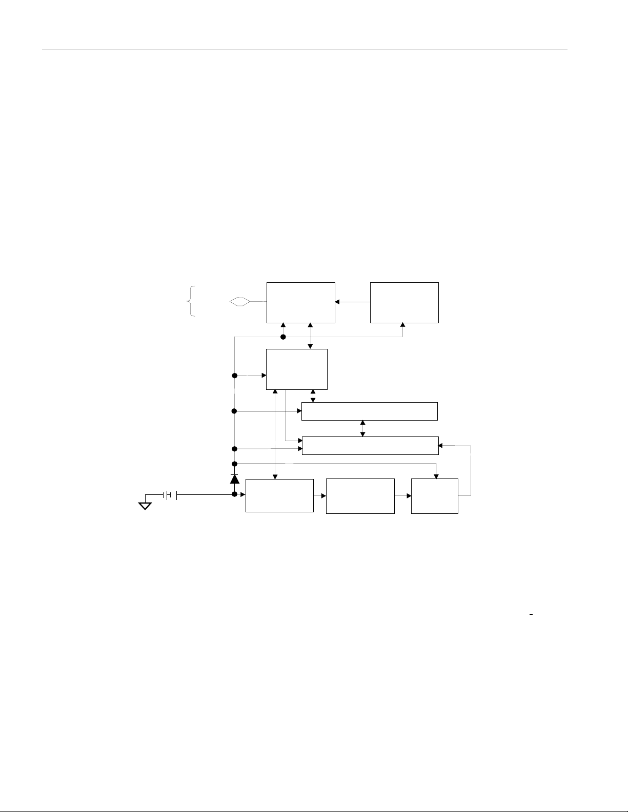
OVERVIEW
The DS1904 has two main data components: 1) 64-bit lasered ROM, and 2) real-time clock counter
(Figure 1). The real-time clock utilizes an on-chip oscillator that is connected to a 32.768 kHz cr ystal.
The hierarchical structure of the 1-Wire protocol is shown in Figure 2.
The bus master must first provide
one of four ROM function commands: 1) Read ROM, 2) Match ROM, 3) Search ROM, 4) Skip ROM.
The protocol for these ROM functions is described in Figure 7. After a ROM function command is
successfully executed, the real-time clock functions become accessible and the master may then provide
one of the real-time clock function commands. The protocol for these commands is described in Figure 5.
All data is read and written least significant bit first.
BLOCK DIAGRAM Figure 1
LID
CONTACT
3V
LITHIUM
DATA
ROM
FUNCTION
CONTROL
CLOCK
FUNCTION
CONTROL
OSCILLATOR
CONTROL
READ/WRITE BUFFER
RTC COUNTER (32-BIT)
32.768 kHz
OSCILLATOR
64-BIT
LASERED
ROM
1 Hz
DIVIDER
64-BIT LASERED ROM
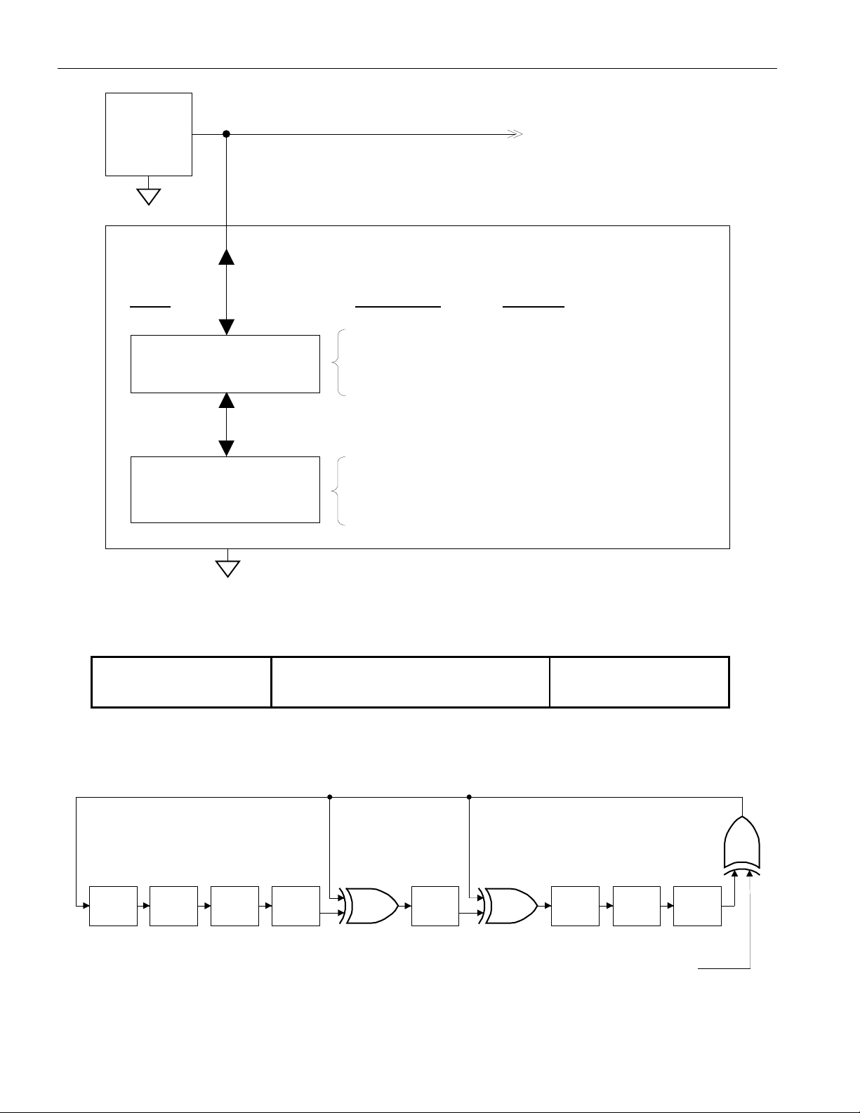
Each DS1904 contains a unique ROM code that is 64 bits long. The first eight bits are a 1-Wire family
code. The next 48 bits are a unique serial number. The last eight bits are a CRC of the first 56 bits. (See
Figure 3.) The 1-Wire CRC is generated using a polynomial generator consisting of a shift register and
XOR gates as shown in Figure 4. The polynomial is X
Dallas Semiconductor 1-Wire Cyclic Redundancy Check is available in the Book of DS19xx iButton
Standards. The shift register bits are initialized to zero. Then starting with the least significant bit of the
family code, one bit at a time is shifted in. After the 8th bit of the family code has been entered, then the
serial number is entered. After the 48th bit of the serial number has been entered, the shift register
contains the CRC value. Shifting in the eight bits of CRC should return the shift register to all zeros. The
64-bit ROM and ROM Function Control section allow the DS1904 to operate as a 1-Wire device and
follow the 1-Wire protocol detailed in the section "1-Wire Bus System".
8
+ X5 + X4 + 1. Additional information about the
2 of 12
Page 3
HIERARCHICAL STRUCTURE FOR 1-WIRE PROTOCOL Figure 2
A
A
(
,
,
p
A
(
DS1904
Bus
Master
Command
Level
1-Wire ROM
Commands
DS1904
Function
see Figure
see Figure
1-Wire Bus
DS1904
vailable
Commands
Read
Match
Search
Ski
Write
Read
Other
Devices
Data Fields
ffected
64-bit
64-bit
64-bit
N/
RTC Counter
RTC Counter
Device
Device
64-BIT LASERED ROM Figure 3
MSB LSB
8-Bit CRC Code 48-Bit Serial Number 8-Bit Family Code (24h)
MSB LSB MSB LSB MSB LSB
1-WIRE CRC GENERATOR Figure 4
Polynomial = X8 + X5 + X4 + 1
0
X
1ST
STAGE
STAGE
1
X
2ND
2
X
3RD
STAGE
3
X
4TH
STAGE
4
X
5TH
STAGE
5
X
R
6TH
STAGE
S
7TH
STAGE
6
X
INPUT DATA
7
X
8TH
STAGE
8
X
3 of 12
Page 4

DS1904
TIMEKEEPING
A 32.768 kHz crystal oscillator is used as the time base for the real-time clock counter. The oscillator can
be turned on or off under software control. The oscillator must be on for the real time clock to function.
The real-time clock counter is double buffered. This allows the master to read time without the data
changing while it is being read. To accomplish this, a snapshot of the counter data is transferred to a
read/write buffer, which the user accesses.
DEVICE CONTROL BYTE
The on/off control of the 32.768 kHz crystal oscillator is done through the device control byte. This byte
can be read and written through the Clock Function commands.
Device Control Byte
76543210
U4 U3 U2 U1
OSC
OSC 0 0
Bit 0 - 1
Bits 0 and 1 are hard-wired to read all 0’s.
Bit 2 - 3
These bits control/report whether the 32.768 kHz crystal oscillator is running. If the os cillator is running,
both OSC bits will read 1. If the oscillator is turned off these bits will all read 0. When writing the device
control byte both occurrences of the OSC bit should have identical data. Otherwise the value in bit address 3 (bold) takes precedence.
Bit 4 - 7
These non-volatile bits have no particular function within the chip. They can be read and written und er
the control of the application software.
0 No function
OSC Oscillator Enable/Disable
Un General-purpose user flags
REAL-TIME CLOCK
The real-time clock is a 32-bit binary counter. It is incremented once per second. The real-time clock can
accumulate 136 years of seconds before rolling over. Time/date is represented by the number of seconds
since a reference point, which is determined by the user. For example, 12:00 a.m., January 1, 1970 could
be a reference point.
CLOCK FUNCTION COMMANDS
The “Clock Function Flow Chart” (Figure 5) describes the protocols necessary for accessing the real-time
clock. With only four bytes of real-time clock and one control byte the DS1904 does not provide random
access. Reading and writing always starts with the device control byte followed by the least significant
byte of the time data.
4 of 12
Page 5

CLOCK FUNCTION COMMAND FLOW CHART Figure 5
Master TX Control
Function Command
DS1904
66H
Read Clock
?
Y
DS1904 copies
RTC Counter
to R/W Buffer
Bus Master RX
Device Control Byte
Bus Master RX
LS Byte (7:0)
Bus Master RX
next Byte (15:8)
Bus Master RX
next Byte (23:16)
N
Device Control Byte
99H
Write Clock
?
Y
Bus Master TX
Bus Master TX
LS Byte (7:0)
Bus Master TX
next Byte (15:8)
Bus Master TX
next Byte (23:16)
Bus Master TX
MS Byte (31:24)
N
Bus Master RX
MS Byte (31:24)
N
Bus Master
TX Reset
?
Y
N
Bus Master
TX Reset
?
Y
DS1904 copies
R/W Buffer
to RTC Counter
DS1904 TX
Presence Pulse
N
Bus Master
TX Reset
?
Y
5 of 12
Page 6

DS1904
READ CLOCK [66h]
The read clock command is used to read the device control byte and the contents of the real-time clock
counter. After having received the most significant bit of the command code the devi ce copies th e actual
contents of the real-time clock counter to the read/write buffer. Now the bus master reads data beginning
with the device control byte followed by the least significant byte through the most significant byte of the
real-time clock. After this the bus master may continue reading from the DS1904. The data received will
be the same as in the first pass through the command flow. The read clock command can be ended at an y
point by issuing a Reset Pulse.
WRITE CLOCK [99h]
The write clock command is used to set the real-time clock counter and to write the device control byte.
After issuing the command, the bus master writes first the device control byte, which becomes immediately effective. After this the bus master sends the least significant byte through the most significant byte
to be written to the real-time clock counter. The new time data is copied from the read/write buffer to the
real-time clock counter and becomes effective as the bus master gener ates a r eset pulse. If the oscillator is
intentionally stopped, the real-time clock counter behaves as a four-byte non-volatile memory.
1-WIRE BUS SYSTEM
The 1-Wire bus is a system, which has a single bus master and one or more slaves. In all instances the
DS1904 is a slave device. The bus master is typically a microcontroller. The discussion of this bus system
is broken down into three topics: hardware configuration, transaction sequence, and 1-Wire signaling
(signal types and timing). A 1-Wire protocol defines bus transactions in terms of the bus state during
specified time slots that are initiated on the falling edge of sync pulses from the bus master. For a more
detailed protocol description, refer to Chapter 4 of the Book of DS19xx iButton Standards.
HARDWARE CONFIGURATION Figure 6
BUS MASTER
Open Drain
RX
TX
Port Pin
V
PUP
5 kΩ
Typ.
RX = RECEIVE
TX = TRANSMIT
DS1904 1-WIRE PORT
DATA
5 µA
Typ.
100 Ω
MOSFET
RX
TX
Hardware Configuration
The 1-Wire bus has only a single line by definition; it is important that each device on the bus be able to
drive it at the appropriate time. To facilitate this, each device attached to the 1-Wire bus must have open
drain or 3-state outputs. The 1-Wire input of the DS1904 is open drain with an internal cir cuit equivalent
to that shown in Figure 6. A multidrop bus consists of a 1-Wire bus with multiple slaves attached. The 1Wire bus has a maximum data rate of 16.3k bits per second and requires a pull-up resistor of approximately 5kΩ.
6 of 12
Page 7

DS1904
The idle state for the 1-Wire bus is high. If for any reason a transaction needs to be suspended, the bus
MUST be left in the idle state if the transaction is to resume. If this does not occur and the bus is left low
for more than 120 µs, one or more of the devices on the bus may be reset. Since the DS1904 gets all its
energy for operation through its VDD pin it will NOT perform a power-on reset if the 1-Wire bus is low
for an extended time period.
Transaction Sequence
The protocol for accessing the DS1904 via the 1-Wire port is as follows:
• Initialization
• ROM Function Command
• Clock Function Command
INITIALIZATION
All transactions on the 1-Wire bus begin with an initialization sequence. The initialization sequence consists of a reset pulse transmitted by the bus master followed by presence pulse(s) transmitted by the
slave(s). The presence pulse lets the bus master know that the DS1904 is on the bus and is ready to
operate. For more details, see the “1-Wire Signaling” section.
ROM FUNCTION COMM ANDS
Once the bus master has detected a presence, it can issue one of the four ROM function commands that
the DS1904 supports. All ROM function commands are eight bits long. A list of these commands follows
(refer to flowchart in Figure 7):
Read ROM [33h]
This command allows the bus master to read the DS1904’s 8-bit family code, unique 48-bit serial number, and 8-bit CRC. This command should only be used if there is a single slave on the bus. If more than
one slave is present on the bus, a data collision will occur when all slaves try to transmit at the same time
(open drain will produce a wired-AND result). The resultant family code and 48-bit serial number read by
the master will be invalid.
Match ROM [55h]
The match ROM command, followed by a 64-bit ROM sequence, allows the bus master to address a specific DS1904 on a multidrop bus. Only the DS1904 that exactly matches the 64-bit ROM sequence will
respond to the following clock function command. All slaves that do not match the 64-bit ROM sequence
will wait for a reset pulse. This command can be used with a single or multiple devices on the bus.
SEARCH ROM [F0h]
When a system is initially brought up, the bus master might not know the number of devices on the 1Wire bus or their 64-bit ROM codes. The search R OM command allows the bus m aster to use a process
of elimination to identify the 64-bit ROM codes of all slave devices on the bus. The search ROM process
is the repetition of a simple 3-step routine: read a bit, read the complement of the bit, then write the desired value of that bit. The bus master performs this 3-step routine on each bit of the ROM. After one
complete pass, the bus master knows the 64-bit ROM code of one device. Additional passes will identify
the ROM codes of the remaining devices. See Chapter 5 of the Book of DS19xx iButton Standards for a
comprehensive discussion of a search ROM, including an actual example.
7 of 12
Page 8

ROM FUNCTIONS FLOW CHART Figure 7
Reset Pulse
DS1904 TX
Presence Pulse
Master TX ROM
Function Command
DS1904
Master TX
33H
Read ROM
Command
?
Y
DS1904 TX
Family Code
1 Byte
DS1904 TX
Serial Number
6 Bytes
N
55H
Match ROM
Command
Master TX Bit 0
Bit 0
Match ?
Master TX Bit 1
Bit 1
Match ?
N
?
Y
NN
Y
NN
F0H
Search ROM
Command
?
Y
DS1904 TX Bit 0
DS1904 TX Bit 0
Master TX Bit 0
Bit 0
Match ?
Y
DS1904 TX Bit 1
DS1904 TX Bit 1
Master TX Bit 1
Bit 1
Match ?
N
CCH
Skip ROM
Command
?
Y
N
DS1904 TX
CRC Byte
Y
Master TX Bit 63
Bit 63
Match ?
Y
DS1904 TX Bit 63
DS1904 TX Bit 63
Master TX Bit 63
NN
Master TX Control
Function Command
(SEE FIGURE 5)
8 of 12
Y
Bit 63
Match ?
Y
Page 9

DS1904
Skip ROM [CCh]
This command can save time in a single drop bus system by allowing the bus master to access the clock
functions without providing the 64-bit ROM code. If more than one slave is present on the bus and, for
example, a read command is issued following the Skip ROM command, data collision will occur on the
bus as multiple slaves transmit simultaneously (open drain pull-downs will produce a wired-AND result).
1–WIRE SIGNALING
The DS1904 requires strict protocols to ensure data integrity. The protocol consists of four types of signaling on one line: Reset Sequence with Reset Pulse and Presence Pulse, Write 0, Write 1 and Read Data.
Except for the presence pulse the bus master initiates all these signals.
The initialization sequence required to begin any communication with the DS1904 is shown in Figure 8.
A reset pulse followed by a presence pulse indicates the DS1904 is ready to send or receive data. The bus
master transmits (TX) a reset pulse (t
, minimum 480 µs). The bus master then releases the line and
RSTL
goes into receive mode (RX). The 1-Wire bus is pulled to a high state via the pull-up resistor. After
detecting the rising edge on the data line, the DS1904 waits (t
presence pulse (t
, 60-240 µs).
PDL
, 15-60 µs) and then transmits the
PDH
INITIALIZATION PROCEDURE “RESET AND PRESENCE PULSES” Figure 8
V
PULLUP
V
PULLUP MIN
V
IH MIN
MASTER TX
"RESET PULSE"
MASTER RX "PRESENCE PULSE"
t
RSTH
V
IL MAX
0V
t
t
RSTL
RESISTOR
MASTER
DS1904
* In order not to mask interrupt signaling by other devices on the 1-Wire bus t
R
480 µs ≤ t
480 µs
15 µs
60
≤
≤
t
≤
t
PDL
t
PDH
< ∞*
RSTL
t
< ∞**
RSTH
< 60 µs
PDH
< 240 µs
t
PDL
+ tR should al-
RSTL
ways be less than 960 µs.
** Includes recovery time
READ/WRITE TIME SLOTS
The definitions of write and read time slots are illustrated in Figure 9. The master initiates all time slots
by driving the data line low. The falling edge of the data line synchronizes the DS1904 to the master by
triggering an internal delay circuit. During write time slots, the delay circuit determines when the DS1904
will sample the data line. For a read data time slot, if a “0” is to be transmitted, the delay circuit determines how long the DS1904 will hold the data line low. If the data bit is a “1”, the DS1904 will not hold
the data line low at all.
9 of 12
Page 10

READ/WRITE TIMING DIAGRAM Figure 9
(
)
(
)
p
g
µ
µ
Write-one Time Slot
DS1904
V
PULLUP
V
PULLUP MI N
V
IH MIN
V
IL MAX
0V
RESISTO
MASTER
Write-zero Time Slot
V
PULLUP
V
PULLUP MIN
V
IH MIN
V
IL MAX
0V
RESISTOR
MASTER
t
LOW1
15µs
OD: 2µs
15µs
(OD: 2µs)
60 µs≤t
s≤t
1
1
s≤t
60 µs ≤ t
1 µs ≤ t
t
SLOT
DS1904
Sam
lin
< 120
< 15 µs
∞
<
SLOT
DS1904
t
LOW0
< t
∞
OD: 6µs
(OD: 6µs)
SLOT
60µs
SLOT
LOW1
REC
t
Sampling Window
60µs
LOW0
<
REC
< 120 µs
t
REC
t
REC
Read-data Time Slot
<
∞
t
REC
t
V
PULLUP
V
PULLUP MIN
V
IH MIN
SLOT
Master
Sampling Window
V
IL MAX
0V
t
RESISTOR
MASTER
DS1904
t
LOWR
SU
t
RDV
60 µs ≤ t
1 µs ≤ t
0 ≤ t
RELEASE
SLOT
LOWR
< 120 µs
< 15 µs
< 45 µs
t
RELEASE
1 µs ≤ t
t
RDV
t
< 1 µs
SU
REC
= 15 µs
10 of 12
Page 11

DS1904
PHYSICAL SPECIFICATION
Size See mechanical drawing
Weight 3.3 grams
Humidity 90% RH at 50°C
Altitude 10000 feet
Expected Service Life 10 years at 25°C
Safety Meets UL#913 (4th Edit.); Intrinsically Safe
Apparatus, Approval under Entity Concept for
use in Class I, Division 1, Group A, B, C and
D Locations (application pending)
ABSOLUTE MAXIMUM RATINGS*
Voltage on 1-Wire to Ground -0.5V to +7.0V
Operating Temperature -40°C to +70°C
Storage Temperature -40°C to +70°C
* This is a stress rating only and functional operation of the device at these or any other conditions
above those indicated in the operation sections of this specification is not implied. Exposure to absolute maximum rating conditions for extended periods of time may affect reliability.
DC ELECTRICAL CHARACTERISTICS (V
=2.8V to 6.0V; -40°C to +70°C)
PUP
PARAMETER SYMBOL MIN TYP MAX UNITS NOTES
Logic 1 V
Logic 0 V
Output Logic Low @ 4 mA V
Output Logic High V
Input Load Current I
IH
IL
OL
OH
L
2.2 6.0 V 1
-0.3 0.8 V 1,5
0.4 V 1
V
PUP
V 1,2
5µA3
CAPACITANCE (tA = 25°C)
PARAMETER SYMBOL MIN TYP MAX UNITS NOTES
Capacitance 1-Wire C
AC ELECTRICAL CHARACTERISTICS (V
IN
=2.8V to 6.0V; -40°C to +70°C)
PUP
PARAMETER SYMBOL MIN TYP MAX UNITS NOTES
Time Slot t
Write 1 Low Time t
Write 0 Low Time t
Read Low Time t
Read Data Valid t
Release Time t
RELEASE
Read Data Setup t
Recovery Time t
Reset High Time t
Reset Low Time t
Presence Detect High t
Presence Detect Low t
SLOT
LOW1
LOW0
LOWR
RDV
SU
REC
RSTH
RSTL
PDH
PDL
60 120 µs
115µs
60 120 µs
115µs
exactly 15 µs 7
01545µs
1µs
480 µs
480 960 µs 6
15 60 µs
60 240 µs
50 pF
1µs 4
11 of 12
Page 12

DS1904
NOTES:
1. All voltages are referenced to ground.
2. V
3. Input load is to ground.
4. Read data setup time refers to the time the host must pull the 1-Wire bus low to read a bit. Data is
5. Under certain low voltage conditions V
6. The reset low time (t
7. The master must read while the data is valid.
= external pull-up voltage.
PUP
guaranteed to be valid within 1 µs of this falling edge.
IL1MAX
may have to be reduced to as much as 0.5V to always
guarantee a presence pulse.
) should be restricted to a maximum of 960 µs, to allow interrupt signaling,
RSTL
otherwise, it could mask or conceal interrupt pulses.
12 of 12
 Loading...