

Page 1
19-5153; Rev 0; 2/10
SFP Controller with Dual LDD Interface
General Description
The DS1876 controls and monitors all functions for
dual transmitter modules. The memory map is based
on SFF-8472. The DS1876 supports APC and modulation control and eye safety functionality for two laser
drivers. It continually monitors for high output current,
high bias current, and low and high transmit power to
ensure that laser shutdown for eye safety requirements
are met without adding external components. Six ADC
channels monitor VCC, temperature, and four external
monitor inputs that can be used to meet all monitoring
requirements.
Applications
Dual Tx Video SFP Modules
Ordering Information
PART TEMP RANGE PIN-PACKAGE
DS1876T+
DS1876T+T&R
+Denotes a lead(Pb)-free/RoHS-compliant package.
T&R = Tape and reel.
*EP = Exposed pad.
-40NC to +95NC
-40NC to +95NC
28 TQFN-EP*
28 TQFN-EP*
Features
S Meets All SFF-8472 Transmitter Control and
Monitoring Requirements
S Six Analog Monitor Channels: Temperature, V
PMON1, BMON1, PMON2, BMON2
PMON_ and BMON_ Support Internal and
External Calibration
Scalable Dynamic Range
Internal Direct-to-Digital Temperature Sensor
Alarm and Warning Flags for All Monitored
Channels
S Six Quick Trips for Fast Monitoring of Critical
Functions for Laser Safety
S Four 10-Bit Delta-Sigma Outputs
Each Controlled by 72-Entry Temperature
Lookup Table (LUT)
S Digital I/O Pins: Six Inputs, Five Outputs
S Comprehensive Fault Measurement System with
Maskable Laser Shutdown Capability
S Flexible, Two-Level Password Scheme Provides
Three Levels of Security
S 256 Additional Bytes Located at A0h Slave
Address
S Transmitter 1 is Accessed at A2h Slave Address
S Transmitter 2 is Accessed at B2h Slave Address
2
S I
C-Compatible Interface
S +2.85V to +3.9V Operating Voltage Range
S -40NC to +95NC Operating Temperature Range
S 28-Pin TQFN (5mm x 5mm x 0.8mm) Package
CC
DS1876
,
_______________________________________________________________ Maxim Integrated Products 1
For pricing, delivery, and ordering information, please contact Maxim Direct at 1-888-629-4642,
or visit Maxim’s website at www.maxim-ic.com.
Page 2

SFP Controller with Dual LDD Interface
TABLE OF CONTENTS
Absolute Maximum Ratings . . . . . . . . . . . . . . . . . . . . . . . . . . . . . . . . . . . . . . . . . . . . . . . . . . . . . . . . . . . . . . . . . . . . . . 5
Recommended Operating Conditions . . . . . . . . . . . . . . . . . . . . . . . . . . . . . . . . . . . . . . . . . . . . . . . . . . . . . . . . . . . . . . 5
DC Electrical Characteristics . . . . . . . . . . . . . . . . . . . . . . . . . . . . . . . . . . . . . . . . . . . . . . . . . . . . . . . . . . . . . . . . . . . . . 5
MOD_, APC_ Electrical Characteristics . . . . . . . . . . . . . . . . . . . . . . . . . . . . . . . . . . . . . . . . . . . . . . . . . . . . . . . . . . . . . 6
DS1876
Analog Quick-Trip Characteristics . . . . . . . . . . . . . . . . . . . . . . . . . . . . . . . . . . . . . . . . . . . . . . . . . . . . . . . . . . . . . . . . . 6
Analog Voltage Monitoring Characteristics . . . . . . . . . . . . . . . . . . . . . . . . . . . . . . . . . . . . . . . . . . . . . . . . . . . . . . . . . . 6
Digital Thermometer Characteristics . . . . . . . . . . . . . . . . . . . . . . . . . . . . . . . . . . . . . . . . . . . . . . . . . . . . . . . . . . . . . . . 7
AC Electrical Characteristics . . . . . . . . . . . . . . . . . . . . . . . . . . . . . . . . . . . . . . . . . . . . . . . . . . . . . . . . . . . . . . . . . . . . . 7
Quick-Trip Timing Characteristics. . . . . . . . . . . . . . . . . . . . . . . . . . . . . . . . . . . . . . . . . . . . . . . . . . . . . . . . . . . . . . . . . . 7
I2C AC Electrical Characteristics . . . . . . . . . . . . . . . . . . . . . . . . . . . . . . . . . . . . . . . . . . . . . . . . . . . . . . . . . . . . . . . . . . 7
Nonvolatile Memory Characteristics. . . . . . . . . . . . . . . . . . . . . . . . . . . . . . . . . . . . . . . . . . . . . . . . . . . . . . . . . . . . . . . . 8
Typical Operating Characteristics . . . . . . . . . . . . . . . . . . . . . . . . . . . . . . . . . . . . . . . . . . . . . . . . . . . . . . . . . . . . . . . . . 9
Pin Configuration . . . . . . . . . . . . . . . . . . . . . . . . . . . . . . . . . . . . . . . . . . . . . . . . . . . . . . . . . . . . . . . . . . . . . . . . . . . . . 10
Pin Description . . . . . . . . . . . . . . . . . . . . . . . . . . . . . . . . . . . . . . . . . . . . . . . . . . . . . . . . . . . . . . . . . . . . . . . . . . . . . . . 10
Block Diagram . . . . . . . . . . . . . . . . . . . . . . . . . . . . . . . . . . . . . . . . . . . . . . . . . . . . . . . . . . . . . . . . . . . . . . . . . . . . . . . 11
Typical Operating Circuit . . . . . . . . . . . . . . . . . . . . . . . . . . . . . . . . . . . . . . . . . . . . . . . . . . . . . . . . . . . . . . . . . . . . . . . 12
Detailed Description . . . . . . . . . . . . . . . . . . . . . . . . . . . . . . . . . . . . . . . . . . . . . . . . . . . . . . . . . . . . . . . . . . . . . . . . . . . 12
DACs During Power-Up . . . . . . . . . . . . . . . . . . . . . . . . . . . . . . . . . . . . . . . . . . . . . . . . . . . . . . . . . . . . . . . . . . . . . . 12
DACs as a Function of Transmit Disable (TXD1, TXD2) . . . . . . . . . . . . . . . . . . . . . . . . . . . . . . . . . . . . . . . . . . . . . . 13
Quick-Trip Timing . . . . . . . . . . . . . . . . . . . . . . . . . . . . . . . . . . . . . . . . . . . . . . . . . . . . . . . . . . . . . . . . . . . . . . . . . . . 13
Monitors and Fault Detection . . . . . . . . . . . . . . . . . . . . . . . . . . . . . . . . . . . . . . . . . . . . . . . . . . . . . . . . . . . . . . . . . . 14
Monitors . . . . . . . . . . . . . . . . . . . . . . . . . . . . . . . . . . . . . . . . . . . . . . . . . . . . . . . . . . . . . . . . . . . . . . . . . . . . . . . . 14
Six Quick-Trip Monitors and Alarms. . . . . . . . . . . . . . . . . . . . . . . . . . . . . . . . . . . . . . . . . . . . . . . . . . . . . . . . . . . 14
Six ADC Monitors and Alarms . . . . . . . . . . . . . . . . . . . . . . . . . . . . . . . . . . . . . . . . . . . . . . . . . . . . . . . . . . . . . . . 14
ADC Timing . . . . . . . . . . . . . . . . . . . . . . . . . . . . . . . . . . . . . . . . . . . . . . . . . . . . . . . . . . . . . . . . . . . . . . . . . . . . . 15
Right-Shifting ADC Result . . . . . . . . . . . . . . . . . . . . . . . . . . . . . . . . . . . . . . . . . . . . . . . . . . . . . . . . . . . . . . . . . . 15
Low-Voltage Operation . . . . . . . . . . . . . . . . . . . . . . . . . . . . . . . . . . . . . . . . . . . . . . . . . . . . . . . . . . . . . . . . . . . . . . . 15
Delta-Sigma Outputs. . . . . . . . . . . . . . . . . . . . . . . . . . . . . . . . . . . . . . . . . . . . . . . . . . . . . . . . . . . . . . . . . . . . . . . . . 16
Digital I/O Pins. . . . . . . . . . . . . . . . . . . . . . . . . . . . . . . . . . . . . . . . . . . . . . . . . . . . . . . . . . . . . . . . . . . . . . . . . . . . . . 18
IN1, RSEL, OUT1, RSELOUT . . . . . . . . . . . . . . . . . . . . . . . . . . . . . . . . . . . . . . . . . . . . . . . . . . . . . . . . . . . . . . . . 18
TXF1, TXF2, TXFOUT, TXD1, TXD2, TXDOUT1, TXDOUT2 . . . . . . . . . . . . . . . . . . . . . . . . . . . . . . . . . . . . . . . . 18
Transmit Fault (TXFOUT) Output . . . . . . . . . . . . . . . . . . . . . . . . . . . . . . . . . . . . . . . . . . . . . . . . . . . . . . . . . . . . . 19
Die Identification . . . . . . . . . . . . . . . . . . . . . . . . . . . . . . . . . . . . . . . . . . . . . . . . . . . . . . . . . . . . . . . . . . . . . . . . . . . . 19
I2C Communication . . . . . . . . . . . . . . . . . . . . . . . . . . . . . . . . . . . . . . . . . . . . . . . . . . . . . . . . . . . . . . . . . . . . . . . . . . . 19
I2C Definitions . . . . . . . . . . . . . . . . . . . . . . . . . . . . . . . . . . . . . . . . . . . . . . . . . . . . . . . . . . . . . . . . . . . . . . . . . . . . . . 19
I2C Protocol. . . . . . . . . . . . . . . . . . . . . . . . . . . . . . . . . . . . . . . . . . . . . . . . . . . . . . . . . . . . . . . . . . . . . . . . . . . . . . . . 21
2 ______________________________________________________________________________________
Page 3

SFP Controller with Dual LDD Interface
TABLE OF CONTENTS (continued)
Memory Organization. . . . . . . . . . . . . . . . . . . . . . . . . . . . . . . . . . . . . . . . . . . . . . . . . . . . . . . . . . . . . . . . . . . . . . . . . . 22
Shadowed EEPROM . . . . . . . . . . . . . . . . . . . . . . . . . . . . . . . . . . . . . . . . . . . . . . . . . . . . . . . . . . . . . . . . . . . . . . . . .23
Register Descriptions . . . . . . . . . . . . . . . . . . . . . . . . . . . . . . . . . . . . . . . . . . . . . . . . . . . . . . . . . . . . . . . . . . . . . . . . . . 24
Memory Map Access Codes . . . . . . . . . . . . . . . . . . . . . . . . . . . . . . . . . . . . . . . . . . . . . . . . . . . . . . . . . . . . . . . . . . 24
Memory Addresses A0h, A2h, and B2h . . . . . . . . . . . . . . . . . . . . . . . . . . . . . . . . . . . . . . . . . . . . . . . . . . . . . . . . . . 24
Lower Memory Register Map . . . . . . . . . . . . . . . . . . . . . . . . . . . . . . . . . . . . . . . . . . . . . . . . . . . . . . . . . . . . . . . . . . 25
Table 01h Register Map . . . . . . . . . . . . . . . . . . . . . . . . . . . . . . . . . . . . . . . . . . . . . . . . . . . . . . . . . . . . . . . . . . . . . . 25
Table 02h Register Map . . . . . . . . . . . . . . . . . . . . . . . . . . . . . . . . . . . . . . . . . . . . . . . . . . . . . . . . . . . . . . . . . . . . . . 26
Table 04h Register Map . . . . . . . . . . . . . . . . . . . . . . . . . . . . . . . . . . . . . . . . . . . . . . . . . . . . . . . . . . . . . . . . . . . . . . 26
Table 05h Register Map . . . . . . . . . . . . . . . . . . . . . . . . . . . . . . . . . . . . . . . . . . . . . . . . . . . . . . . . . . . . . . . . . . . . . . 27
Table 06h Register Map . . . . . . . . . . . . . . . . . . . . . . . . . . . . . . . . . . . . . . . . . . . . . . . . . . . . . . . . . . . . . . . . . . . . . . 27
Auxiliary Memory A0h Register Map . . . . . . . . . . . . . . . . . . . . . . . . . . . . . . . . . . . . . . . . . . . . . . . . . . . . . . . . . . . . 27
Lower Memory Register Descriptions. . . . . . . . . . . . . . . . . . . . . . . . . . . . . . . . . . . . . . . . . . . . . . . . . . . . . . . . . . . . 28
Table 01h Register Descriptions . . . . . . . . . . . . . . . . . . . . . . . . . . . . . . . . . . . . . . . . . . . . . . . . . . . . . . . . . . . . . . . . 40
Table 02h Register Descriptions . . . . . . . . . . . . . . . . . . . . . . . . . . . . . . . . . . . . . . . . . . . . . . . . . . . . . . . . . . . . . . . . 44
Table 04h Register Descriptions . . . . . . . . . . . . . . . . . . . . . . . . . . . . . . . . . . . . . . . . . . . . . . . . . . . . . . . . . . . . . . . . 64
Table 06h Register Descriptions . . . . . . . . . . . . . . . . . . . . . . . . . . . . . . . . . . . . . . . . . . . . . . . . . . . . . . . . . . . . . . . . 65
Auxiliary Memory A0h Register Descriptions . . . . . . . . . . . . . . . . . . . . . . . . . . . . . . . . . . . . . . . . . . . . . . . . . . . . . . 68
Applications Information. . . . . . . . . . . . . . . . . . . . . . . . . . . . . . . . . . . . . . . . . . . . . . . . . . . . . . . . . . . . . . . . . . . . . . . . 69
Power-Supply Decoupling. . . . . . . . . . . . . . . . . . . . . . . . . . . . . . . . . . . . . . . . . . . . . . . . . . . . . . . . . . . . . . . . . . . . .69
SDA and SCL Pullup Resistors . . . . . . . . . . . . . . . . . . . . . . . . . . . . . . . . . . . . . . . . . . . . . . . . . . . . . . . . . . . . . . . . . 69
Package Information. . . . . . . . . . . . . . . . . . . . . . . . . . . . . . . . . . . . . . . . . . . . . . . . . . . . . . . . . . . . . . . . . . . . . . . . . . . 69
DS1876
_______________________________________________________________________________________ 3
Page 4

SFP Controller with Dual LDD Interface
LIST OF FIGURES
Figure 1. Power-Up Timing . . . . . . . . . . . . . . . . . . . . . . . . . . . . . . . . . . . . . . . . . . . . . . . . . . . . . . . . . . . . . . . . . . . . . . 13
Figure 2. TXD1, TXD2 Timing. . . . . . . . . . . . . . . . . . . . . . . . . . . . . . . . . . . . . . . . . . . . . . . . . . . . . . . . . . . . . . . . . . . . 13
Figure 3. Quick-Trip Sample Timing . . . . . . . . . . . . . . . . . . . . . . . . . . . . . . . . . . . . . . . . . . . . . . . . . . . . . . . . . . . . . . . 14
Figure 4. ADC Round-Robin Timing. . . . . . . . . . . . . . . . . . . . . . . . . . . . . . . . . . . . . . . . . . . . . . . . . . . . . . . . . . . . . . . 15
DS1876
Figure 5. Low-Voltage Hysteresis Example . . . . . . . . . . . . . . . . . . . . . . . . . . . . . . . . . . . . . . . . . . . . . . . . . . . . . . . . . 16
Figure 6. Recommended RC Filter for DAC Outputs in Voltage Mode and Current Sink Mode . . . . . . . . . . . . . . . . . 16
Figure 7. 3-Bit (8-Position) Delta-Sigma Example . . . . . . . . . . . . . . . . . . . . . . . . . . . . . . . . . . . . . . . . . . . . . . . . . . . . 17
Figure 8. DAC OFFSET LUTs . . . . . . . . . . . . . . . . . . . . . . . . . . . . . . . . . . . . . . . . . . . . . . . . . . . . . . . . . . . . . . . . . . . . 17
Figure 9. Logic Diagram 1 . . . . . . . . . . . . . . . . . . . . . . . . . . . . . . . . . . . . . . . . . . . . . . . . . . . . . . . . . . . . . . . . . . . . . . 18
Figure 10. Logic Diagram 2 . . . . . . . . . . . . . . . . . . . . . . . . . . . . . . . . . . . . . . . . . . . . . . . . . . . . . . . . . . . . . . . . . . . . . 18
Figure 11a. TXFOUT Nonlatched Operation . . . . . . . . . . . . . . . . . . . . . . . . . . . . . . . . . . . . . . . . . . . . . . . . . . . . . . . . 19
Figure 11b. TXFOUT Latched Operation . . . . . . . . . . . . . . . . . . . . . . . . . . . . . . . . . . . . . . . . . . . . . . . . . . . . . . . . . . . 19
Figure 12. I2C Timing . . . . . . . . . . . . . . . . . . . . . . . . . . . . . . . . . . . . . . . . . . . . . . . . . . . . . . . . . . . . . . . . . . . . . . . . . . 20
Figure 13. Example I2C Timing . . . . . . . . . . . . . . . . . . . . . . . . . . . . . . . . . . . . . . . . . . . . . . . . . . . . . . . . . . . . . . . . . . 21
Figure 14. Memory Map . . . . . . . . . . . . . . . . . . . . . . . . . . . . . . . . . . . . . . . . . . . . . . . . . . . . . . . . . . . . . . . . . . . . . . . . 23
LIST OF TABLES
Table 1. Acronyms . . . . . . . . . . . . . . . . . . . . . . . . . . . . . . . . . . . . . . . . . . . . . . . . . . . . . . . . . . . . . . . . . . . . . . . . . . . . 13
Table 2. ADC Default Monitor Full-Scale Ranges . . . . . . . . . . . . . . . . . . . . . . . . . . . . . . . . . . . . . . . . . . . . . . . . . . . . 14
4 ______________________________________________________________________________________
Page 5

SFP Controller with Dual LDD Interface
ABSOLUTE MAXIMUM RATINGS
Voltage Range on PMON_, BMON_, RSEL,
IN1, TXF_, and TXD_ Pins
Relative to Ground ...............................-0.5V to (VCC + 0.5V)*
Voltage Range on VCC, SDA, SCL,
OUT1, RSELOUT, and TXFOUT Pins
Relative to Ground ...............................................-0.5V to +6V
*Subject to not exceeding +6V.
Stresses beyond those listed under “Absolute Maximum Ratings” may cause permanent damage to the device. These are stress ratings only, and functional
operation of the device at these or any other conditions beyond those indicated in the operational sections of the specifications is not implied. Exposure to absolute
maximum rating conditions for extended periods may affect device reliability.
RECOMMENDED OPERATING CONDITIONS
(TA = -40NC to +95NC, unless otherwise noted.)
PARAMETER SYMBOL CONDITIONS MIN TYP MAX UNITS
Main Supply Voltage V
High-Level Input Voltage
(SDA, SCL)
Low-Level Input Voltage
(SDA, SCL)
High-Level Input Voltage
(TXD_, TXF_, RSEL, IN1)
Low-Level Input Voltage
(TXD_, TXF_, RSEL, IN1)
V
V
V
V
CC
IH:1
IL:1
IH:2
IL:2
(Note 1) +2.85 +3.9 V
Continuous Power Dissipation
28-Pin TQFN (derate 34.5mW/°C) above +70°C ....2758.6mW
Operating Temperature Range .......................... -40NC to +95NC
Programming Temperature Range ....................... 0NC to +95NC
Storage Temperature Range ............................ -55NC to +125NC
Soldering Temperature .........................Refer to the IPC/JEDEC
J-STD-020 Specification.
0.7 x
V
CC
-0.3
2.0
-0.3 +0.8 V
VCC +
0.3
0.3 x
V
CC
VCC +
0.3
V
V
V
DS1876
DC ELECTRICAL CHARACTERISTICS
(VCC = +2.85V to +3.9V, TA = -40NC to +95NC, unless otherwise noted.)
PARAMETER SYMBOL CONDITIONS MIN TYP MAX UNITS
Supply Current I
Output Leakage (SDA, OUT1,
RSELOUT, TXFOUT)
Low-Level Output Voltage
(SDA, OUT1, RSELOUT,
TXDOUT_, MOD_, APC_,
TXFOUT)
High-Level Output Voltage
(MOD_, APC_, TXDOUT_)
TXDOUT_ Before EEPROM
Recall
MOD_, APC_ Before Recall Figure 1 10 100 nA
Input Leakage Current
(SCL, TXD_, RSEL, IN1, TXF_)
Digital Power-On Reset POD 1.0 2.2 V
Analog Power-On Reset POA 2.0 2.75 V
_______________________________________________________________________________________ 5
CC
I
LO
V
OL
V
OH
I
LI
(Notes 1, 2) 2.5 10 mA
1
IOL = 4mA 0.4
IOL = 6mA 0.6
IOH = 4mA
VCC -
0.4
10 100 nA
1
FA
V
V
FA
Page 6
SFP Controller with Dual LDD Interface
MOD_, APC_ ELECTRICAL CHARACTERISTICS
(VCC = +2.85V to +3.9V, TA = -40NC to +95NC, unless otherwise noted.)
PARAMETER SYMBOL CONDITIONS MIN TYP MAX UNITS
Main Oscillator Frequency f
Delta-Sigma Input-Clock
Frequency
DS1876
Reference Voltage Input (REFIN) V
Output Range 0 V
Output Resolution
Output Impedance R
OSC
f
DS
REFIN
DS
Minimum 0.1FF to GND
See the Delta-Sigma Outputs section for
details
2 V
ANALOG QUICK-TRIP CHARACTERISTICS
(VCC = +2.85V to +3.9V, TA = -40NC to +95NC, unless otherwise noted.)
PARAMETER SYMBOL CONDITIONS MIN TYP MAX UNITS
TXP HI, TXP LO Full-Scale
Voltage
HBIAS Full-Scale Voltage 1.25 V
PMON_ Input Resistance 35 50 65
Resolution 8 Bits
Error
Integral Nonlinearity -1 +1 LSB
Differential Nonlinearity -1 +1 LSB
Temperature Drift -2.5 +2.5 %FS
Offset -5 +10 mV
TA = +25°C ±2
5 MHz
f
/2 MHz
OSC
CC
REFIN
10 Bits
35 100
2.507 V
V
V
I
kW
%FS
ANALOG VOLTAGE MONITORING CHARACTERISTICS
(VCC = +2.85V to +3.9V, TA = -40NC to +95NC, unless otherwise noted.)
PARAMETER SYMBOL CONDITIONS MIN TYP MAX UNITS
ADC Resolution 13 Bits
Input/Supply Accuracy
(BMON_, PMON_, VCC)
Update Rate for Temperature,
BMON_, PMON_, VCC
Input/Supply Offset
(BMON_, PMON_, VCC)
Factory Setting (Note 4)
6 ______________________________________________________________________________________
ACC At factory setting 0.25 0.5 %FS
t
RR
V
OS
(Note 3) 0 5 LSB
BMON_, PMON_ 2.5
VCC 6.5536
64 78 ms
V
Page 7
SFP Controller with Dual LDD Interface
DIGITAL THERMOMETER CHARACTERISTICS
(VCC = +2.85V to +3.9V, TA = -40NC to +95NC, unless otherwise noted.)
PARAMETER SYMBOL CONDITIONS MIN TYP MAX UNITS
Thermometer Error T
ERR
AC ELECTRICAL CHARACTERISTICS
(VCC = +2.85V to +3.9V, TA = -40NC to +95NC, unless otherwise noted.)
PARAMETER SYMBOL CONDITIONS MIN TYP MAX UNITS
TXD_ Enable t
Recovery from TXD_ Disable
(Figure 2)
Fault Reset Time (to TXFOUT = 0)
Fault Assert Time (to TXFOUT = 1) t
OFF
t
ON
t
INITR1
t
INITR2
FAULT
QUICK-TRIP TIMING CHARACTERISTICS
(VCC = +2.85V to +3.9V, TA = -40NC to +95NC, unless otherwise noted.)
PARAMETER SYMBOL CONDITIONS MIN TYP MAX UNITS
Output-Enable Time Following POA t
Sample Time per Quick-Trip
Comparison
-40NC to +95NC
From ↑ TXD_
From ↓ TXD_
From ↓ TXD_
On power-up or ↓ TXD_, when VCC LO
alarm is detected (Note 5)
After HTXP_, LTXP_, HBATH_ 1.6 10.5
INIT
t
REP
-3 +3
131
161
20 ms
1.6
NC
5
1 ms
Fs
ms
Fs
Fs
DS1876
I2C AC ELECTRICAL CHARACTERISTICS
(VCC = +2.85V to +3.9V, TA = -40NC to +95NC, timing referenced to V
Communication section.)
PARAMETER SYMBOL CONDITIONS MIN TYP MAX UNITS
SCL Clock Frequency f
Clock Pulse-Width Low t
Clock Pulse-Width High t
Bus Free Time Between STOP and
START Condition
START Hold Time t
START Setup Time t
Data Out Hold Time t
Data In Setup Time t
Rise Time of Both SDA and SCL
Signals
Fall Time of Both SDA and SCL
Signals
STOP Setup Time t
Capacitive Load for Each Bus Line C
EEPROM Write Time t
_______________________________________________________________________________________ 7
HIGH
t
HD:STA
SU:STA
HD:DAT
SU:DAT
SU:STO
SCL
LOW
BUF
t
t
WR
(Note 6) 0 400 kHz
0.6
(Note 7)
R
(Note 7)
F
B
(Note 8) 20 ms
IL(MAX)
and V
, unless otherwise noted. See the I2C
IH(MIN)
1.3
0.6
1.3
0.6
0 0.9
100 ns
20 +
0.1C
20 +
0.1C
0.6
B
B
300 ns
300 ns
400 pF
Fs
Fs
Fs
Fs
Fs
Fs
Fs
Page 8
SFP Controller with Dual LDD Interface
NONVOLATILE MEMORY CHARACTERISTICS
(VCC = +2.85V to +3.9V, unless otherwise noted.)
PARAMETER SYMBOL CONDITIONS MIN TYP MAX UNITS
EEPROM Write Cycles
DS1876
Note 1: All voltages are referenced to ground. Current into the IC is positive, and current out of the IC is negative.
Note 2: Inputs are at supply rail. Outputs are not loaded.
Note 3: This parameter is guaranteed by design.
Note 4: Full scale is user programmable.
Note 5: A temperature conversion is completed and MOD1 DAC, MOD2 DAC, APC1 DAC, and APC2 DAC values are recalled
from the LUT and VCC has been measured to be above VCC LO alarm, if the VCC LO alarm is enabled.
Note 6: I2C interface timing shown is for fast-mode (400kHz) operation. This device is also backward compatible with I2C stan-
dard mode.
Note 7: CB—Total capacitance of one bus line in pF.
Note 8: EEPROM write begins after a STOP condition occurs.
At +25NC
At +85NC
200,000
50,000
8 ______________________________________________________________________________________
Page 9
SFP Controller with Dual LDD Interface
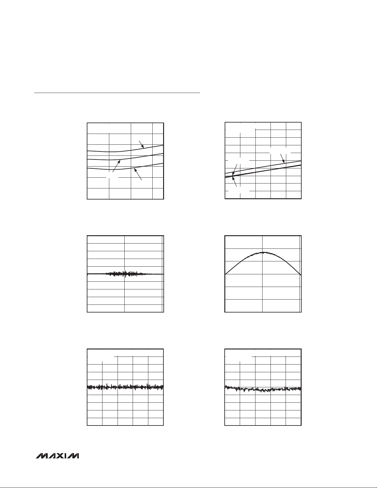
Typical Operating Characteristics
(V
CC
= 3.3V, T
= +25°C, unless otherwise noted.)
A
DS1876
SUPPLY CURRENT vs. SUPPLY VOLTAGE
2.7
SDA = SCL = V
DACs AT 1FFh
2.6
2.5
2.4
2.3
SUPPLY CURRENT (mA)
2.2
2.1
2.0
2.850
CC
+95°C
+25°C
VCC (V)
APC1/2 AND MOD1/2 DAC DNL
1.0
0.8
0.6
0.4
0.2
0
-0.2
-0.4
-0.6
APC1/2 AND MOD1/2 DAC DNL (LSB)
-0.8
-1.0
0
DAC POSITION (DEC)
-40°C
SUPPLY CURRENT vs. TEMPERATURE
3.0
DAC POSITIONS = 1FFh
2.9
DS1876 toc01
3.7503.4503.150
SDA = SCL = V
2.8
2.7
2.6
VCC = 3.3V
2.5
2.4
2.3
SUPPLY CURRENT (mA)
2.2
VCC = 2.85V
2.1
2.0
-40 85
CC
VCC = 3.9V
TEMPERATURE (°C)
DS1876 toc02
603510-15
APC1/2 AND MOD1/2 DAC INL
3
DS1876 toc03
1000500
2
1
0
-1
APC1/2 AND MOD1/2 DAC INL (LSB)
-2
-3
0
DAC POSITION (DEC)
DS1876 toc04
1000500
1.0
PMON1/2 AND BMON1/2 DNL
USING FACTORY-PROGRAMMED FULL-SCALE
0.8
VALUE OF 2.5V
0.6
0.4
0.2
0
-0.2
-0.4
-0.6
PMON1/2 AND BMON1/2 DNL (LSB)
-0.8
-1.0
0 2.5
PMON1/2 AND BMON1/2 INPUT VOLTAGE (V)
1.0
DS1876 toc05
2.01.51.00.5
0.8
0.6
0.4
0.2
-0.2
-0.4
-0.6
PMON1/2 AND BMON1/2 INL (LSB)
-0.8
-1.0
PMON1/2 AND BMON1/2 INL
USING FACTORY-PROGRAMMED FULL-SCALE
VALUE OF 2.5V
0
0 2.5
PMON1/2 AND BMON1/2 INPUT VOLTAGE (V)
2.01.51.00.5
DS1876 toc06
_______________________________________________________________________________________ 9
Page 10
SFP Controller with Dual LDD Interface
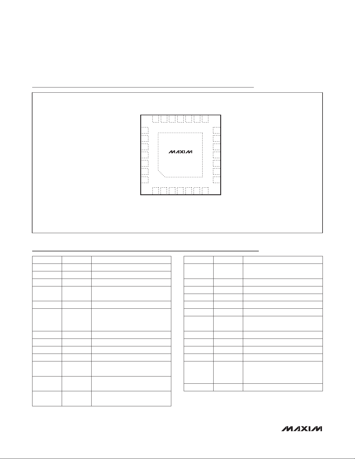
Pin Configuration
TOP VIEW
MOD2
MOD1
GND
2021 19 17 16 15
GND
18
CC
TXDOUT2
V
N.C.
DS1876
IN1
TXD1
14
13
12
11
10
9
8
BMON1
PMON1
BMON2
PMON2
TXDOUT1
RSEL
GND
CC
External Monitor Input BMON1
and HBATH1 Quick Trip
Power-Supply Input
Reference Input for DAC1 and
DAC2
Digital Output. General-purpose
output, AS1 output in SFF-8079,
or RS1 output in SFF-8431.
REFIN
22
TXD2
23
24
APC2
25
APC1
V
TXF2
OUT1
26
CC
27
28
1 2
RSELOUT
DS1876
+
3
SCL
SDA
*EP
4 5 6 7
TXF1
TXFOUT
THIN QFN
(5mm
× 5mm × 0.8mm)
*EXPOSED PAD.
Pin Description
PIN NAME FUNCTION
1 RSELOUT Rate-Select Output
2 SCL I2C Serial-Clock Input
3 SDA I2C Serial-Data Input/Output
4 TXFOUT
Transmit Fault Output, Open
Drain
5 TXF1 Transmit Fault Input 1
Digital Input. General-purpose
6 IN1
input, AS1 in SFF-8079, or RS1
in SFF-8431.
7 TXD1 Transmit Disable Input 1
8, 18, 21 GND Ground Connection
9 RSEL Rate-Select Input
10 TXDOUT1 Transmit Disable Output 1
11 PMON2
12 BMON2
13 PMON1
External Monitor Input PMON2
and HTXP2/LTXP2 Quick Trip
External Monitor Input BMON2
and HBATH2 Quick Trip
External Monitor Input PMON1
and HTXP1/LTXP1 Quick Trip
PIN NAME FUNCTION
14 BMON1
15 N.C. No Connection
16, 26 V
17 TXDOUT2 Transmit Disable Output 2
19 MOD2 MOD2 DAC, Delta-Sigma Output
20 MOD1 MOD1 DAC, Delta-Sigma Output
22 REFIN
23 TXD2 Transmit Disable Input 2
24 APC2 APC2 DAC, Delta-Sigma Output
25 APC1 APC1 DAC, Delta-Sigma Output
27 TXF2 Transmit Fault Input 2
28 OUT1
— EP Exposed Pad (Connect to GND)
10 _____________________________________________________________________________________
Page 11
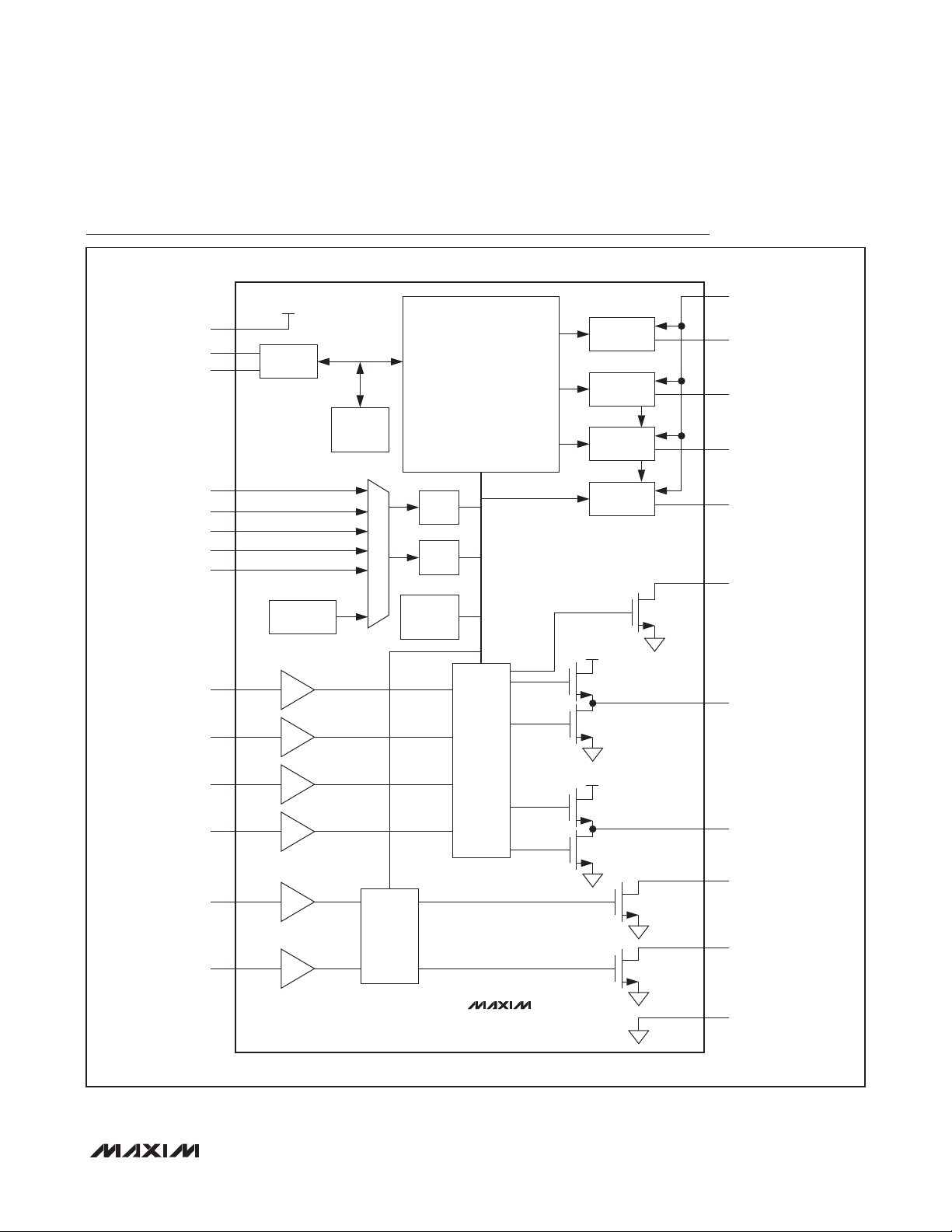
SFP Controller with Dual LDD Interface
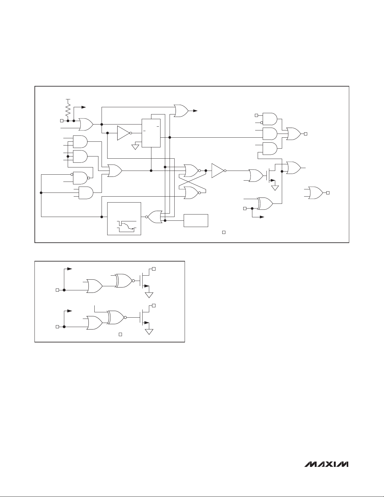
Block Diagram
DS1876
V
SDA
SCL
V
BMON1
PMON1
BMON2
PMON2
TXD1
TXD2
TXF1
V
CC
CC
I2C
INTERFACE
EEPROM
256 BYTES
AT A0h
CC
ANALOG MUX
TEMPERATURE
SENSOR
MAIN MEMORY
EEPROM/SRAM
A/D CONFIGURATION/RESULTS,
SYSTEM STATUS/CONTROL BITS,
ALARMS/WARNINGS,
LOOKUP TABLES,
USER MEMORY
13-BIT
ADC
8-BIT
QTs
POWER-ON
ANALOG
INTERRUPT
LOGIC
CONTROL
MOD2 DAC
APC2 DAC
MOD1 DAC
APC1 DAC
V
CC
V
CC
10 BITS
10 BITS
10 BITS
10 BITS
REFIN
MOD2
APC2
MOD1
APC1
TXFOUT
TXDOUT1
TXF2
RSEL
LOGIC
CONTROL
IN1
DS1876
TXDOUT2
RSELOUT
OUT1
GND
______________________________________________________________________________________ 11
Page 12
SFP Controller with Dual LDD Interface
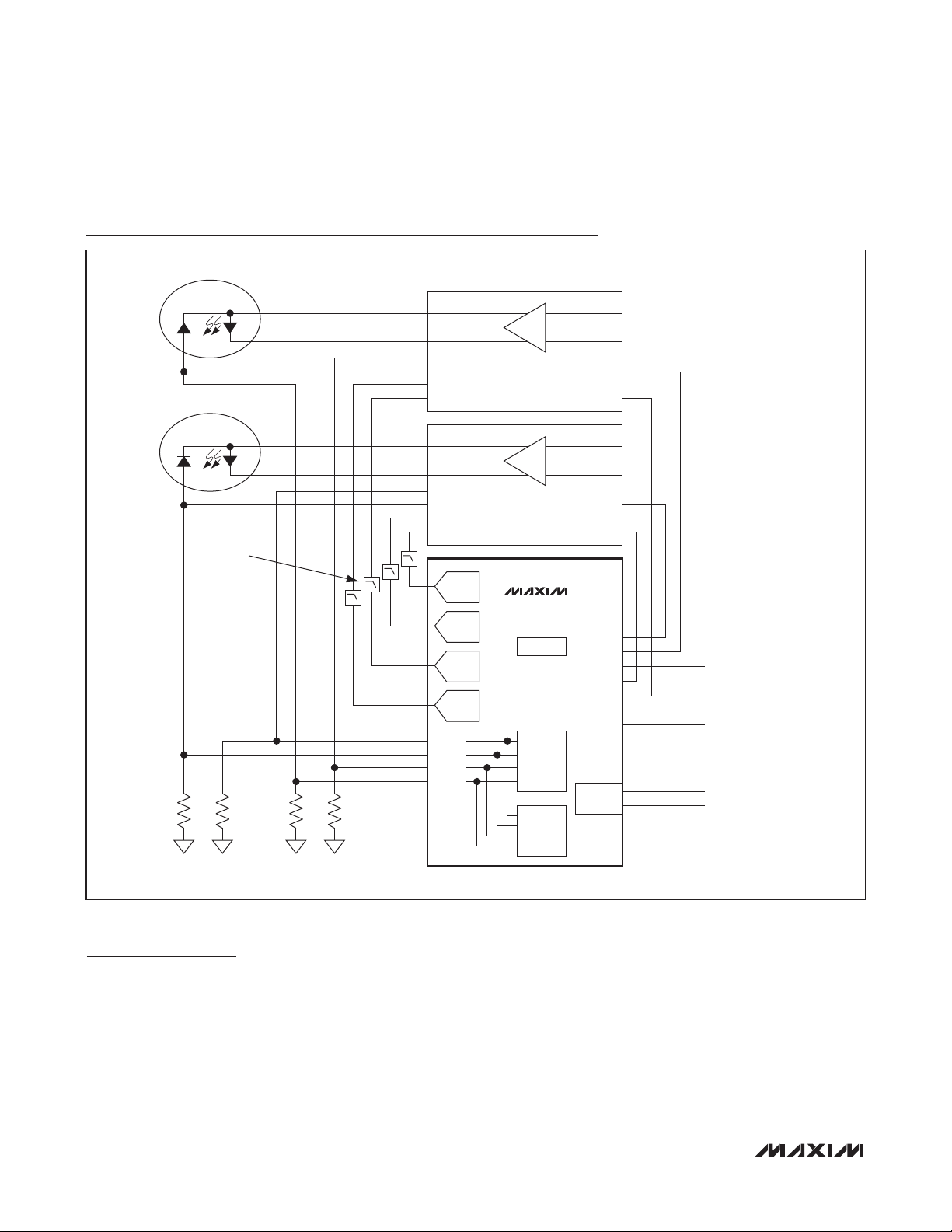
Typical Operating Circuit
TOSA2
DS1876
R
P1
TOSA1
RC FILTERS
(FIGURE 6)
R
B1
LDD2
BMON
APCIN
APCSET
MODSET
LDD1
BMON
APCIN
APCSET
MODSET
MOD1
DAC
APC1
DAC
MOD2
DAC
APC2
DAC
BMON1
PMON1
BMON2
PMON2
R
R
B1
P2
DS1876
EEPROM
QUICK
TRIP
ADC
FAULT
DISABLE
FAULT
DISABLE
TXF1
TXF2
TXFOUT
TXDOUT1
TXDOUT2
TXD1
TXD2
SDA
I2C
SCL
TX_FAULT
TX_DISABLE1
TX_DISABLE2
MODE_DEF2 (SDA)
MODE_DEF1 (SCL)
Detailed Description
The DS1876 integrates the control and monitoring functionality required in a dual transmitter system. Key components of the DS1876 are shown in the Block Diagram
and described in subsequent sections.
DACs During Power-Up
On power-up, the DS1876 sets the DACs to high impedance. After time t
, the DACs are set to an initial condition
INIT
set in EEPROM. After a temperature conversion is completed and if the VCC LO alarm is enabled, an additional
VCC conversion above the customer-defined VCC LO
alarm level is required before the DACs are updated with
the value determined by the temperature conversion and
the DAC LUT.
If a fault is detected, and TXD1 and TXD2 are toggled
to re-enable the outputs, the DS1876 powers up following a similar sequence to an initial power-up. The
12 _____________________________________________________________________________________
Page 13
SFP Controller with Dual LDD Interface
Table 1. Acronyms
ACRONYM DESCRIPTION
ADC Analog-to-Digital Converter
AGC Automatic Gain Control
APC Automatic Power Control
APD Avalanche Photodiode
ATB Alarm Trap Bytes
DAC Digital-to-Analog Converter
LOS Loss of Signal
LUT Lookup Table
NV Nonvolatile
QT Quick Trip
TE Tracking Error
TIA Transimpedance Amplifier
ROSA Receiver Optical Subassembly
SEE Shadowed EEPROM
SFF Small Form Factor
SFF-8472
SFP Small Form Factor Pluggable
SFP+ Enhanced SFP
TOSA Transmit Optical Subassembly
TXP Transmit Power
Document Defining Register Map of SFPs
and SFFs
only difference is that the DS1876 already has determined the present temperature, so the t
time is not
INIT
required for the DS1876 to recall the APC and MOD
set points from EEPROM. See Figure 1.
DACs as a Function of Transmit Disable
(TXD1, TXD2)
If TXD1 or TXD2 are asserted (logic 1) during normal
operation, the associated outputs are disabled within
t
. When TXD1 or TXD2 are deasserted (logic 0), the
OFF
DS1876 sets the DACs with the value associated with
the present temperature. When asserted, soft TXD1 or
soft TXD2 (TXDC) (Lower Memory, Register 6Eh) would
allow a software control identical to the TXD1 or TXD2 pin
(Figure 2). The POLARITY register (Table 02h, Register
C6h) determines if the off-state value of the DACs is
V
or 0V.
REFIN
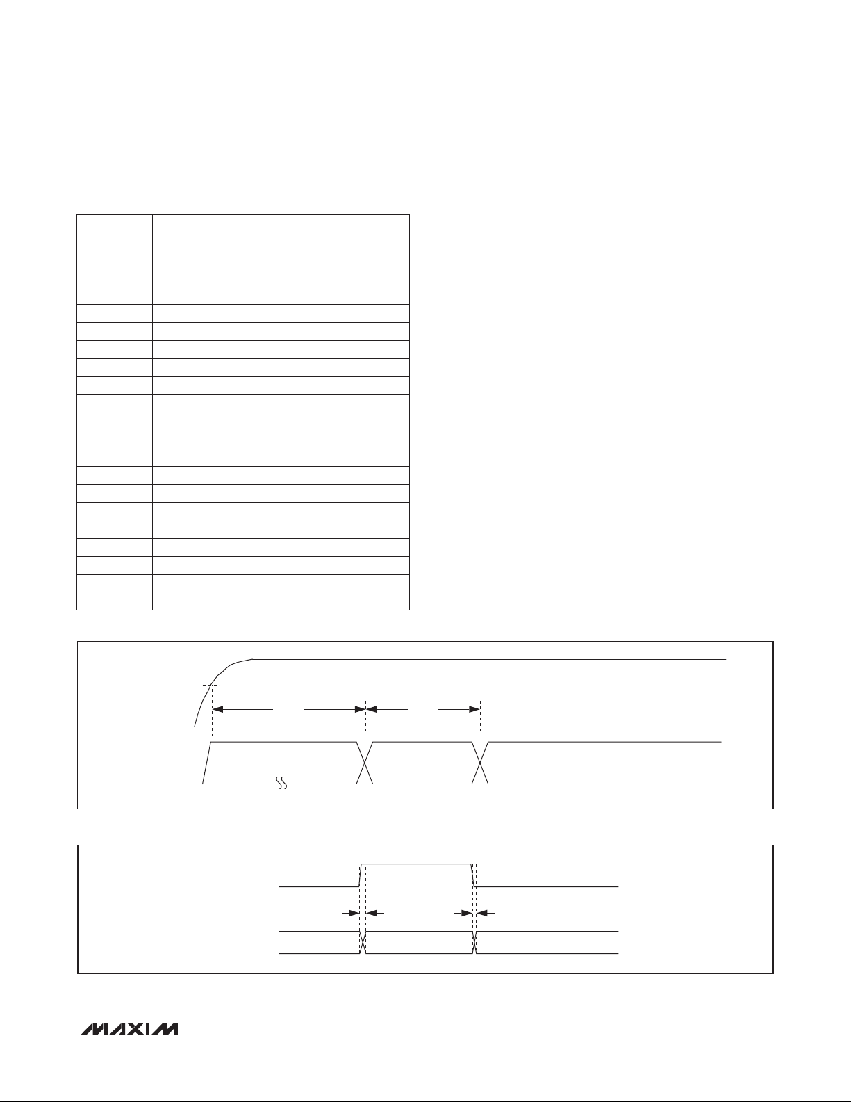
Quick-Trip Timing
As shown in Figure 3, the DS1876’s input comparator is shared among the six quick-trip alarms (TXP1
HI, TXP1 LO, TXP2 HI, TXP2 LO, BIAS1 HI, and BIAS2
HI). The comparator polls the alarms in a multiplexed
sequence. The updates are used to compare the HTXP1,
LTXP1, HTXP2, and LTXP2 (monitor diode voltages) and
the HBATH1 and HBATH2 (BMON1, BMON2) signals
against the internal APC and BIAS reference, respectively. Depending on the results of the comparison, the
DS1876
V
CC
DAC
SETTINGS
Figure 1. Power-Up Timing
Figure 2. TXD1, TXD2 Timing
______________________________________________________________________________________ 13
V
POA
500µs
HIGH IMPEDANCE OFF STATE LUT VALUE
TXD_
DAC
SETTINGS
LUT VALUE LUT VALUEOFF STATE
t
INIT
t
OFF
t
ON
Page 14
SFP Controller with Dual LDD Interface
QT CYCLE
QUICK-TRIP SAMPLE TIMES
DS1876
Figure 3. Quick-Trip Sample Timing
LTXP2
SAMPLE
HBIAS1
SAMPLE
t
REP
HBIAS2
SAMPLE
HTXP1
SAMPLE
HTXP2
SAMPLE
LTXP1
SAMPLE
LTXP2
SAMPLE
HBIAS1
SAMPLE
Table 2. ADC Default Monitor Full-Scale Ranges
SIGNAL (UNITS) +FS SIGNAL +FS HEX -FS SIGNAL -FS HEX
Temperature (NC)
VCC (V) 6.5528 FFF8 0 0000
PMON1, PMON2 and BMON1, BMON2 (V) 2.4997 FFF8 0 0000
corresponding alarms and warnings (TXP HI1, TXP LO1,
TXP HI2, TXP LO2, BIAS HI1, and BIAS HI2) are asserted
or deasserted.
After resetting, the device completes one QT cycle
before making comparisons. The TXP LO quick-trip
alarm updates its alarm bit, but does not create FETG
until after TXD
figured to wait for TXD
. TXP HI and BIAS HI can also be con-
EXT
; however, this can be disabled
EXT
using QTHEXT_ (Table 02h, Register 88h).
Monitors and Fault Detection
Monitoring functions on the DS1876 include six quicktrip comparators and six ADC channels. This monitoring
combined with the alarm enables (Table 01h/05h) determines when/if the DS1876 turns off DACs and triggers
the TXFOUT and TXDOUT1, TXDOUT2 outputs. All the
monitoring levels and interrupt masks are user programmable.
Six Quick-Trip Monitors and Alarms
Six quick-trip monitors are provided to detect potential
laser safety issues and LOS status. These monitor the
following:
1) High Bias Current 1 (HBATH1), causing QT BIAS1 HI
2) Low Transmit Power 1 (LTXP1), causing QT TXP1 LO
3) High Transmit Power 1 (HTXP1), causing QT TXP1 HI
4) High Bias Current 2 (HBATH2), causing QT BIAS2 HI
5) Low Transmit Power 2 (LTXP2), causing QT TXP2 LO
6) High Transmit Power 2 (HTXP2), causing QT TXP2 HI
127.996 7FFF -128 8000
The high and low transmit power quick-trip registers
(HTXP1, HTXP2, LTXP1, and LTXP2) set the thresholds
used to compare against the PMON1 and PMON2 voltages to determine if the transmit power is within specification. The HBATH1 and HBATH2 QTs compare the
BMON1 and BMON2 inputs (generally from the laser
driver’s bias monitor output) against their threshold settings to determine if the present bias current is above
specification. The bias and power QTs are routed to
FETG through interrupt masks to allow combinations
of these alarms to be used to trigger FETG. The bias
Monitors
and power QTs are directly connected to TXFOUT (see
Figure 9). The user can program up to eight different
temperature-indexed threshold levels for HBATH1 and
HBATH2 (Table 06h, Registers E0h-E7h).
Six ADC Monitors and Alarms
The ADC monitors six channels that measure temperature (internal temp sensor), VCC, PMON1, PMON2,
BMON1, and BMON2 using an analog multiplexer to
measure them round-robin with a single ADC (see the
ADC Timing section). The channels have a customerprogrammable full-scale range, and all channels have a
customer-programmable offset value that is factory programmed to a default value (see Table 2). Additionally,
PMON1, PMON2 and BMON1, BMON2 can right-shift
results by up to 7 bits before the results are compared
to alarm thresholds or read over the I2C bus. This allows
customers with specified ADC ranges to calibrate the
ADC full scale to a factor of 1/2n of their specified range
to measure small signals. The DS1876 can then rightshift the results by n bits to maintain the bit weight of their
specification.
14 _____________________________________________________________________________________
Page 15
SFP Controller with Dual LDD Interface
The ADC results (after right-shifting, if used) are compared to the alarm and warning thresholds after each
conversion, and the corresponding alarms are set that
can be used to trigger the TXFOUT output. These ADC
thresholds are user programmable, as are the masking
registers that can be used to prevent the alarms from triggering the TXFOUT output.
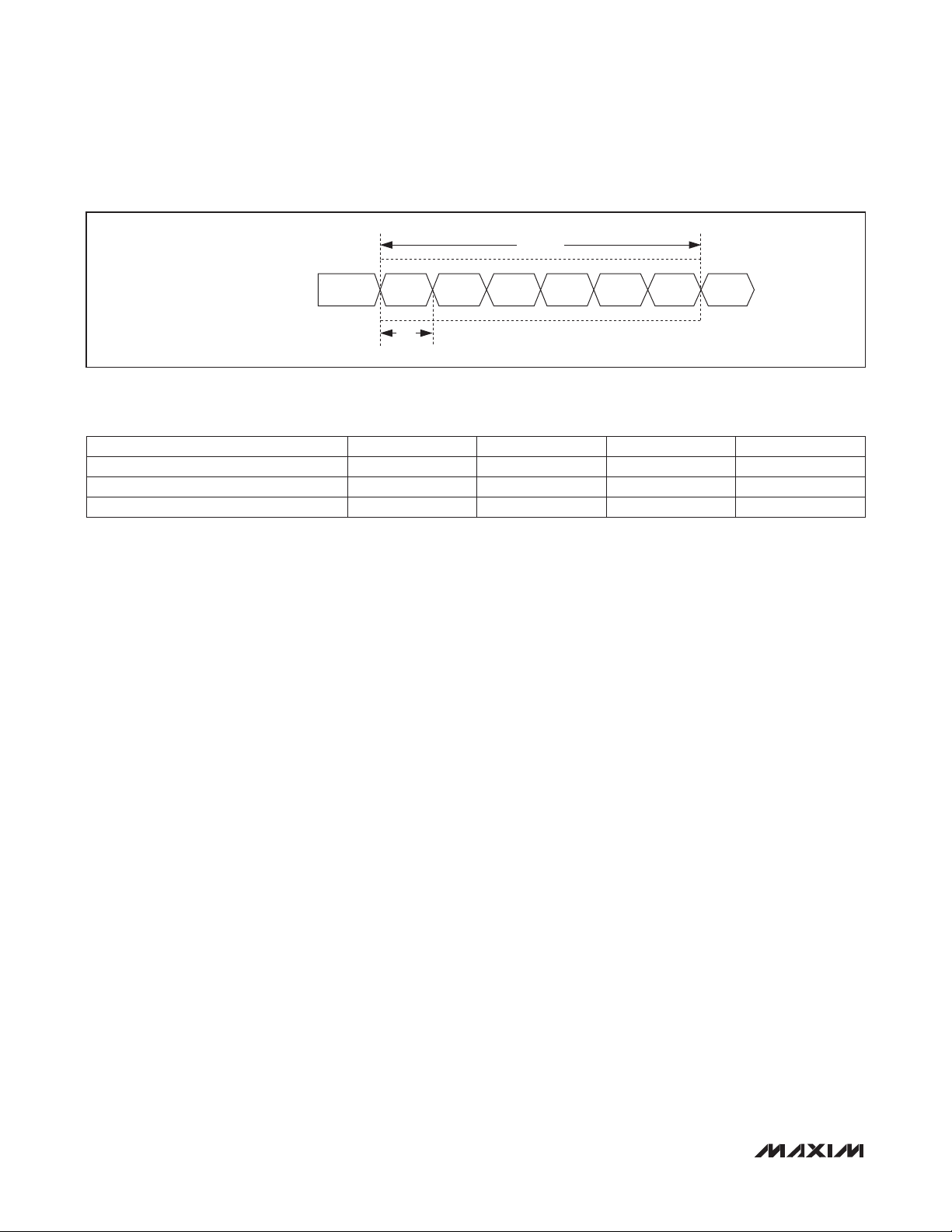
ADC Timing
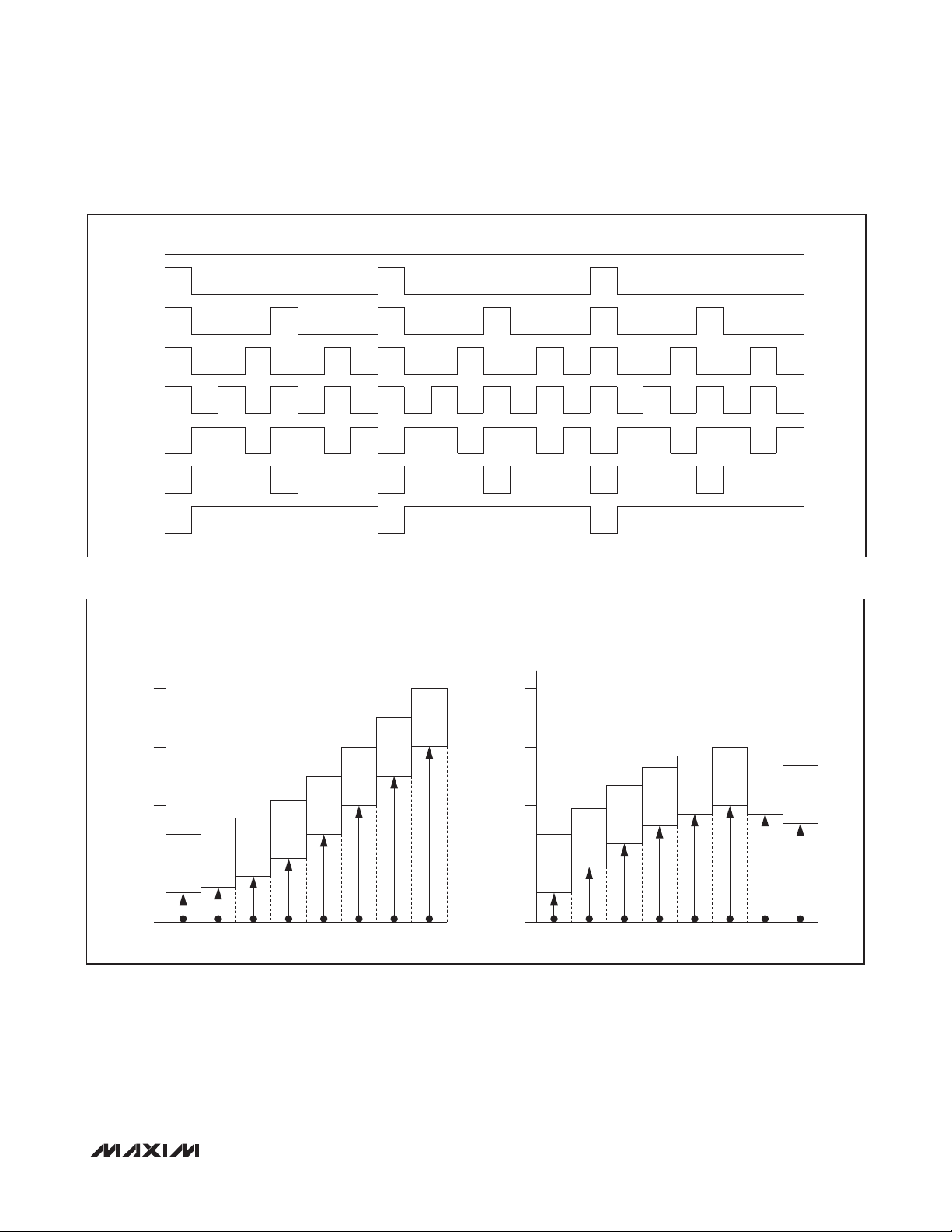
There are six analog channels that are digitized in a
round-robin fashion in the order as shown in Figure 4.
The total time required to convert all six channels is tRR
(see the Analog Voltage Monitoring Characteristics table
for details).
Right-Shifting ADC Result
If the weighting of the ADC digital reading must conform
to a predetermined full-scale (PFS) value defined by
a standard’s specification (e.g., SFF-8472), then rightshifting can be used to adjust the PFS analog measurement range while maintaining the weighting of the ADC
results. The DS1876’s range is wide enough to cover all
requirements; when the maximum input value is P 1/2
the FS value, right-shifting can be used to obtain greater
accuracy. For instance, the maximum voltage might be
1/8 the specified PFS value, so only 1/8 of the converter’s
range is effective over this range. An alternative is to calibrate the ADC’s full-scale range to 1/8 the readable PFS
value and use a right-shift value of 3. With this implementation, the resolution of the measurement is increased by
a factor of 8, and because the result is digitally divided
by 8 by right-shifting, the bit weight of the measurement
still meets the standard’s specification (i.e., SFF-8472).
The right-shift operation on the ADC result is carried
out based on the contents of right-shift control registers
(Table 02h, Registers 8Eh-8Fh) in EEPROM. Four analog
channels—PMON1, PMON2, BMON1, and BMON2—
each have 3 bits allocated to set the number of right-
shifts. Up to seven right-shift operations are allowed and
DS1876
are executed as a part of every conversion before the
results are compared to the high and low alarm levels, or
loaded into their corresponding measurement registers
(Lower Memory, Registers 64h–6Bh). This is true during
the setup of internal calibration as well as during subsequent data conversions.
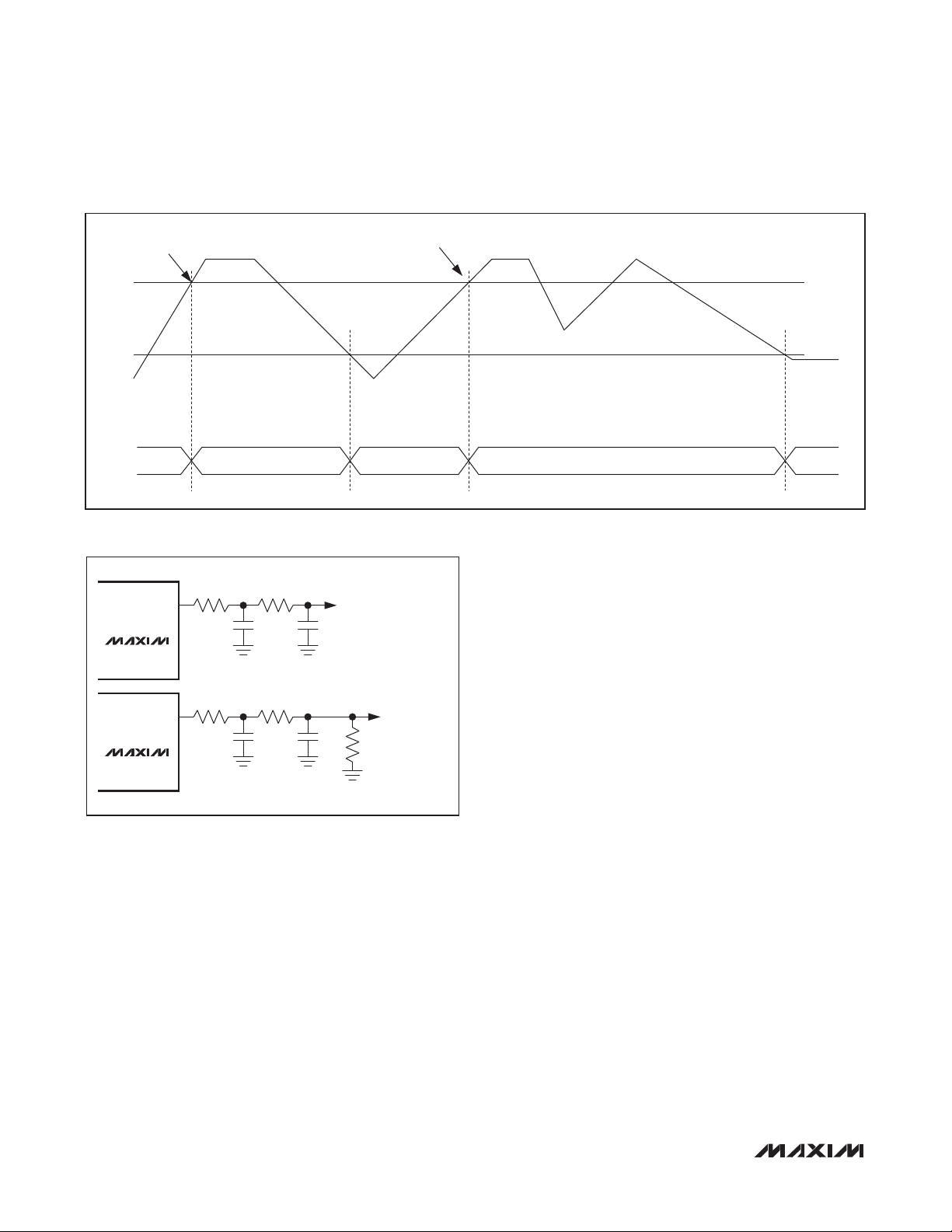
Low-Voltage Operation
The DS1876 contains two power-on reset (POR) levels.
The lower level is a digital POR (POD) and the higher
level is an analog POR (POA). At startup, before the supply voltage rises above POA, the outputs are disabled,
all SRAM locations are set to their defaults, shadowed
EEPROM (SEE) locations are zero, and all analog circuitry is disabled. When VCC reaches POA, the SEE is
recalled, and the analog circuitry is enabled. While VCC
remains above POA, the device is in its normal operating
state, and it responds based on its nonvolatile configuration. If during operation VCC falls below POA, but is
still above POD, the SRAM retains the SEE settings from
the first SEE recall, but the device analog is shut down
and the outputs disabled. If the supply voltage recovers
back above POA, the device immediately resumes normal operation. If the supply voltage falls below POD, the
device SRAM is placed in its default state and another
SEE recall is required to reload the nonvolatile settings.
The EEPROM recall occurs the next time VCC next
exceeds POA. Figure 5 shows the sequence of events
as the voltage varies.
Any time VCC is above POD, the I2C interface can be
used to determine if VCC is below the POA level. This
is accomplished by checking the RDYB bit in the status
byte (Lower Memory, Register 6Eh). RDYB is set when
VCC is below POA; when VCC rises above POA, RDYB
is timed (within 500Fs) to go to 0, at which point the part
is fully functional.
ONE ROUND-ROBIN ADC CYCLE
TEMP V
NOTE: IF THE VCC LO ALARM IS ENABLED AT POWER-UP, THE ADC ROUND-ROBIN TIMING CYCLES BETWEEN TEMPERATURE AND VCC ONLY UNTIL VCC IS ABOVE THE VCC LO
ALARM THRESHOLD. THIS ALSO OCCURS IF THERE ARE BOTH A TXD1 EVENT AND A TXD2 EVENT UNDER THE SAME CONDITIONS AS PREVIOUSLY MENTIONED.
Figure 4. ADC Round-Robin Timing
______________________________________________________________________________________ 15
BMON1 BMON2 PMON1 PMON2 TEMP
CC
t
RR
Page 16
SFP Controller with Dual LDD Interface
SEE RECALL
V
POA
V
CC
SEE RECALL
DS1876
V
POD
PRECHARGED
SEE RECALLED VALUE RECALLED VALUE
TO 0
Figure 5. Low-Voltage Hysteresis Example
3.24kΩ 3.24kΩ
DAC
0.01µF 0.01µF
DS1876
1kΩ 1kΩ
DAC
0.1µF 0.1µF
DS1876
Figure 6. Recommended RC Filter for DAC Outputs in Voltage
Mode and Current Sink Mode
For all device addresses sourced from EEPROM (Table
02h, Register 8Bh), the default device addresses are
A2h and B2h until VCC exceeds POA allowing the device
address to be recalled from the EEPROM.
Delta-Sigma Outputs
Four delta-sigma outputs are provided: MOD1, MOD2,
APC1, and APC2. With the addition of an external RC
filter, these outputs provide 10-bit resolution analog
outputs with the full-scale range set by the input REFIN.
Each output is either manually controlled or controlled
using a temperature-indexed LUT.
PRECHARGED TO 0
VOLTAGE OUTPUT
CURRENT SINK
2kΩ
A delta-sigma DAC has a digital output using pulsedensity modulation. It provides much lower output ripple
than a standard digital PWM output given the same clock
rate and filter components. Before t
are high impedance. The external RC filter components
are chosen based on ripple requirements, output load,
delta-sigma frequency, and desired response time.
Figure 6 shows a recommended filter.
For illustrative purposes, a 3-bit example is provided in
Figure 7.
In LUT mode the DACs are each controlled by an LUT
with high-temperature resolution and an OFFSET LUT
with lower temperature resolution. The high-resolution
LUTs each have 2NC resolutions. The OFFSET LUTs
are located in the upper eight registers (F8h-FFh) of
the table containing each high-resolution LUT. The DAC
values are determined as follows:
DAC value = LUT + 4 x (OFFSET LUT)
An example calculation for MOD1 DAC is as follows:
Assumptions:
1) Temperature is +43NC
2) Table 04h (MOD1 OFFSET LUT), Register FCh = 2Ah
3) Table 04h (MOD1 LUT), Register AAh = 7Bh
Because the temperature is +43NC, the MOD1 LUT index
is AAh and the MOD1 OFFSET LUT index is FCh.
MOD1 DAC = 7Bh + 4 x 2Ah = 123h = 291
PRECHARGED
, the DAC outputs
INIT
TO 0
16 _____________________________________________________________________________________
Page 17
SFP Controller with Dual LDD Interface
O
1
2
3
4
5
6
7
Figure 7. 3-Bit (8-Position) Delta-Sigma Example
DS1876
DAC OFFSET LUTs (04h/06h)[A2h/B2h]
EIGHT REGISTERS PER DAC
EACH OFFSET REGISTER CAN BE INDEPENDENTLY
1023
SET BETWEEN 0 AND 1020. 1020 = 4 x FFh. THIS
EXAMPLE ILLUSTRATES POSITIVE TEMPCO.
FCh
DAC
LUT
BITS
7:0
FDh
DAC
LUT
BITS
7:0
767
511
DELTA-SIGMA DACs
255
0
-40°C -8°C +8°C +24°C +40°C +56°C +70°C +88°C +104°C
F8h
DAC
LUT
BITS
7:0
F9h
DAC
LUT
BITS
7:0
FAh
DAC
LUT
BITS
7:0
FBh
DAC
LUT
BITS
7:0
FEh
DAC
LUT
BITS
7:0
FFh
DAC
LUT
BITS
7:0
Figure 8. DAC OFFSET LUTs
When temperature controlled, the DACs are updated
after each temperature conversion.
The reference input, REFIN, is the supply voltage for the
output buffer of all four DACs. The voltage connected to
DAC OFFSET LUTs (04h/06h)[A2h/B2h]
EIGHT REGISTERS PER DAC
EACH OFFSET REGISTER CAN BE INDEPENDENTLY SET BETWEEN
1023
0 AND 1020. 1020 = 4 x FFh. THIS EXAMPLE ILLUSTRATES POSITIVE
AND NEGATVE TEMPCO.
767
F8h
DAC
LUT
BITS
7:0
F9h
DAC
LUT
BITS
7:0
511
DELTA-SIGMA DACs
255
0
-40°C -8°C +8°C +24°C +40°C +56°C +70°C +88°C +104°C
FAh
DAC
LUT
BITS
7:0
FBh
DAC
LUT
BITS
7:0
FCh
DAC
LUT
BITS
7:0
FDh
DAC
LUT
BITS
7:0
FEh
DAC
LUT
BITS
7:0
FFh
DAC
LUT
BITS
7:0
REFIN and its decoupling must be able to support the
edge rate requirements of the delta-sigma outputs. In
a typical application, a 0.1FF capacitor should be connected between REFIN and ground.
______________________________________________________________________________________ 17
Page 18
SFP Controller with Dual LDD Interface
V
CC
R
PU
TXD_
TXDC_
DS1876
TXP_ HI FLAG
TXP HI ENABLE
HBAL_ FLAG
HBAL ENABLE
TXDS_
R
C
Q
C
Q
D
S
SET BIAS_ DAC AND
MOD_ DAC TO HIGH
IMPEDANCE
FETG_
TXD_
TXDIO_
TXDFG_
TXDFLT_
TXDOUT_
TXFOUTS_
QTHEXT_
TXP_ LO FLAG
TXP LO ENABLE
FAULT RESET TIMER
TXD
(t
)
EXT
INITR1
(130ms)
OUT IN
IN
OUT
Figure 9. Logic Diagram 1
IN1S OUT1
INVOUT1
IN1C
IN1
INVRSOUT
RSELS
RSELC
RSEL
= PINS
RSELOUT
Figure 10. Logic Diagram 2
Digital I/O Pins
Six digital input pins and five digital output pins are provided for monitoring and control.
IN1, RSEL, OUT1, RSELOUT
Digital input pins IN1 and RSEL primarily serve to meet
the rate-select requirements of SFP and SFP+. They
can also serve as general-purpose inputs. OUT1 and
RSELOUT are driven by a combination of the IN1, RSEL,
and logic dictated by control registers in the EEPROM
(see Figure 10). The levels of IN1 and RSEL can be
read from the STATUS register (Lower Memory, Register
6Eh). The open-drain output OUT1 can be controlled
and/or inverted using the CNFGB register (Table 02h,
TXFINT
TXFOUTS1
TXFOUTS2
POWER-ON
RESET
INVTXF_
TXF_
NOTE:
_ CAN BE EITHER 1 OR 2 CORRESPONDING TO TRANSMITTERS 1 OR 2.
REFERS TO A PIN.
TXFS_
Register 89h). The open-drain RSELOUT output is
software controlled and/or inverted through the STATUS
register and CNFGA register (Table 02h, Register 88h).
External pullup resistors must be provided on OUT1 and
RSELOUT to realize high logic levels.
TXF1, TXF2, TXFOUT, TXD1, TXD2,
TXDOUT1, TXDOUT2
TXDOUT1 and TXDOUT2 are generated from a combination of TXF1, TXF2, TXD1, TXD2, and the internal
signals FETG1 and FETG2 (Table 02h, Register 8Ah). A
software control identical to TXD1 and TXD2 is also available (TXDC1 and TXDC2, Lower Memory, Register 6Eh).
A TXD1 or TXD2 pulse is internally extended (TXD
by time t
to inhibit the latching of low alarms and
INITR1
warnings related to the APC loop to allow for the loop to
stabilize. The nonlatching alarms and warnings are TXP
LO, BMON1 LO, BMON2 LO, PMON1 LO, and PMON2
LO. In addition, TXP LO is disabled from creating FETG.
See the Transmit Fault (TXFOUT) Output section for a
detailed explanation of TXFOUT. As shown in Figure 9,
the same signals and faults can also be used to generate the internal signal FETG. FETG is used to send a fast
“turn-off” command to the laser driver. The intended use
is a direct connection to the laser driver’s TXD1, TXD2
input if this is desired. When VCC < POA, TXDOUT1 and
TXDOUT2 are high impedance.
TXFOUT
EXT
)
18 _____________________________________________________________________________________
Page 19
SFP Controller with Dual LDD Interface
DETECTION OF TXFOUT FAULT
TXFOUT
Figure 11a. TXFOUT Nonlatched Operation
DETECTION OF TXFOUT FAULT
TXD_ OR TXFOUT RESET
TXFOUT
Figure 11b. TXFOUT Latched Operation
DS1876
Transmit Fault (TXFOUT) Output
TXFOUT can be triggered by all alarms, warnings, QTs,
TXD1, TXD2, TXF1, and TXF2 (see Figure 9). The six
ADC alarms and warnings are controlled by enable bits
(Table 01h/05h, Registers F8h and FCh). See Figures
11a and 11b for nonlatched and latched operation for
TXFOUT. The CNFGB register (Table 02h, Register 89h)
controls the latching of the alarms.
Die Identification
The DS1876 has an ID hardcoded in its memory. Two
registers (Table 02h, Registers 86h-87h) are assigned
for this feature. Register 86h reads 76h to identify the
part as the DS1876; Register 87h reads the present
device version.
I2C Communication
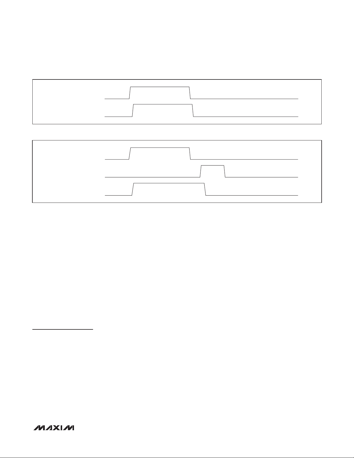
I2C Definitions
The following terminology is commonly used to describe
I2C data transfers.
Master Device: The master device controls the slave
devices on the bus. The master device generates SCL
clock pulses and START and STOP conditions.
Slave Devices: Slave devices send and receive data
at the master’s request.
Bus Idle or Not Busy: Time between STOP and
START conditions when both SDA and SCL are inactive and in their logic-high states.
START Condition: A START condition is generated
by the master to initiate a new data transfer with a
slave. Transitioning SDA from high to low while SCL
remains high generates a START condition. See
Figure 12 for applicable timing.
STOP Condition: A STOP condition is generated
by the master to end a data transfer with a slave.
Transitioning SDA from low to high while SCL remains
high generates a STOP condition. See Figure 12 for
applicable timing.
Repeated START Condition: The master can use
a repeated START condition at the end of one data
transfer to indicate that it will immediately initiate a
new data transfer following the current one. Repeated
STARTs are commonly used during read operations
to identify a specific memory address to begin a data
transfer. A repeated START condition is issued identically to a normal START condition. See Figure 12 for
applicable timing.
Bit Write: Transitions of SDA must occur during the
low state of SCL. The data on SDA must remain valid
and unchanged during the entire high pulse of SCL
plus the setup and hold time requirements (Figure 12).
Data is shifted into the device during the rising edge
of the SCL.
Bit Read: At the end of a write operation, the master
must release the SDA bus line for the proper amount
of setup time (Figure 12) before the next rising edge
______________________________________________________________________________________ 19
Page 20
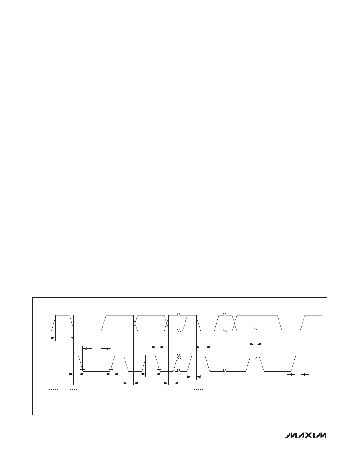
SFP Controller with Dual LDD Interface
of SCL during a bit read. The device shifts out each
bit of data on SDA at the falling edge of the previous
SCL pulse and the data bit is valid at the rising edge
of the current SCL pulse. Remember that the master
generates all SCL clock pulses, including when it is
reading bits from the slave.
DS1876
Acknowledgement (ACK and NACK): An acknowledgement (ACK) or not-acknowledge (NACK) is
always the 9th bit transmitted during a byte transfer.
The device receiving data (the master during a read
or the slave during a write operation) performs an ACK
by transmitting a zero during the 9th bit. A device performs a NACK by transmitting a one during the 9th bit.
Timing (Figure 12) for the ACK and NACK is identical
to all other bit writes. An ACK is the acknowledgment
that the device is properly receiving data. A NACK is
used to terminate a read sequence or as an indication
that the device is not receiving data.
Byte Write: A byte write consists of 8 bits of information transferred from the master to the slave (most
significant bit first) plus a 1-bit acknowledgement from
the slave to the master. The 8 bits transmitted by the
master are done according to the bit write definition
and the acknowledgement is read using the bit read
definition.
Byte Read: A byte read is an 8-bit information transfer
from the slave to the master plus a 1-bit ACK or NACK
from the master to the slave. The 8 bits of information
that are transferred (most significant bit first) from the
slave to the master are read by the master using the
bit read definition, and the master transmits an ACK
using the bit write definition to receive additional data
bytes. The master must NACK the last byte read to
terminate communication so the slave returns control
of SDA to the master.
Slave Address Byte: Each slave on the I2C bus
responds to a slave address byte sent immediately
following a START condition. The slave address byte
contains the slave address in the most significant 7 bits
and the R/W bit in the least significant bit.
The DS1876 responds to three slave addresses. The
auxiliary memory always responds to a fixed I2C slave
address, A0h. (If the main device’s slave address
is programmed to be A0h, access to the auxiliary
memory is disabled.) The Lower Memory and Tables
00h–06h respond to I2C slave addresses whose lower
3 bits are configurable (A0h–AEh, B0h-BEh) using the
DEVICE ADDRESS byte (Table 02h, Register 8Bh). The
user also must set the ASEL bit (Table 02h, Register
88h) for this address to be active. By writing the correct slave address with R/W = 0, the master indicates
it writes data to the slave. If R/W = 1, the master reads
data from the slave. If an incorrect slave address is
written, the DS1876 assumes the master is communicating with another I2C device and ignores the communications until the next START condition is sent.
Memory Address: During an I2C write operation
to the DS1876, the master must transmit a memory
address to identify the memory location where the
slave is to store the data. The memory address is
SDA
t
BUF
t
LOW
SCL
t
HD:STA
STOP START REPEATED
NOTE: TIMING IS REFERENCED TO V
IL(MAX)
AND V
IH(MIN)
t
R
t
HD:DAT
.
t
HIGH
t
F
t
SU:DAT
START
t
SU:STA
t
HD:STA
t
SP
Figure 12. I2C Timing
20 _____________________________________________________________________________________
t
SU:STO
Page 21
SFP Controller with Dual LDD Interface
always the second byte transmitted during a write
operation following the slave address byte.
I2C Protocol
See Figure 13 for an example of I2C timing.
Writing a Single Byte to a Slave: The master must
generate a START condition, write the slave address
byte (R/W = 0), write the memory address, write
the byte of data, and generate a STOP condition.
Remember that the master must read the slave’s
acknowledgement during all byte write operations.
Writing Multiple Bytes to a Slave: To write multiple
bytes to a slave, the master generates a START condition, writes the slave address byte (R/W = 0), writes
the memory address, writes up to 8 data bytes, and
generates a STOP condition. The DS1876 writes 1 to
8 bytes (one page or row) with a single write transaction. This is internally controlled by an address
counter that allows data to be written to consecutive
addresses without transmitting a memory address
before each data byte is sent. The address counter
limits the write to one 8-byte page (one row of the
memory map). Attempts to write to additional pages
of memory without sending a STOP condition between
pages result in the address counter wrapping around
to the beginning of the present row.
For example: A 3-byte write starts at address 06h and
DS1876
writes three data bytes (11h, 22h, and 33h) to three
“consecutive” addresses. The result is that addresses
06h and 07h would contain 11h and 22h, respectively, and the third data byte, 33h, would be written
to address 00h.
To prevent address wrapping from occurring, the
master must send a STOP condition at the end of
the page, then wait for the bus-free or EEPROM write
time to elapse. Then the master can generate a new
START condition and write the slave address byte
(R/W = 0) and the first memory address of the next
memory row before continuing to write data.
Acknowledge Polling: Any time a EEPROM page is
written, the DS1876 requires the EEPROM write time
(tWR) after the STOP condition to write the contents of
the page to EEPROM. During the EEPROM write time,
the DS1876 does not acknowledge its slave address
because it is busy. It is possible to take advantage
of that phenomenon by repeatedly addressing the
DS1876, which allows the next page to be written
as soon as the DS1876 is ready to receive the data.
The alternative to acknowledge polling is to wait for
maximum period of tWR to elapse before attempting
to write again to the DS1876.
2
TYPICAL I
C WRITE TRANSACTION
MSB LSB
START
X X X X 0 0 1 R/W
SLAVE
ADDRESS*
*IF ASEL IS 0, THE SLAVE ADDRESS IS A0h FOR THE AUXILIARY MEMORY AND A2h/B2h FOR THE MAIN MEMORY.
IF ASEL = 1, THE SLAVE ADDRESS IS DETERMINED BY TABLE 02h, REGISTER 8Bh FOR THE MAIN MEMORY. THE AUXILIARY MEMORY CONTINUES TO BE ADDRESSED AT A0h, EXCEPT WHEN THE PROGRAMMED
ADDRESS FOR THE MAIN MEMORY IS A0h.
2
EXAMPLE I
C TRANSACTIONS WITH A2h AS THE SLAVE ADDRESS
A)
SINGLE-BYTE WRITE
-WRITE 00h TO REGISTER BAh
B)
SINGLE-BYTE READ
-READ REGISTER BAh
C)
TWO-BYTE WRITE
-WRITE 01h AND 75h TO
REGISTERS C8h AND C9h
D)
TWO-BYTE READ
-READ C8h AND C9h
START STOP
START
START
START
READ/
WRITE
A2h
1 0 1 0 0 0 1 0
A2h
1 0 1 0 0 0 1 0
A2h
1 0 1 0 0 0 1 0
A2h
1 0 1 0 0 0 1 0
MSB LSB
SLAVE
b7 b6 b5 b4 b3 b2 b1 b0
ACK
REGISTER ADDRESS
SLAVE
ACK
SLAVE
ACK
SLAVE
ACK
SLAVE
ACK
BAh
1 0 1 1 1 0 1 0
BAh
1 0 1 1 1 0 1 0
C8h
1 1 0 0 1 0 0 0
C8h
1 1 0 0 1 0 0 0
SLAVE
ACK
SLAVE
ACK
SLAVE
ACK
SLAVE
ACK
00h
0 0 0 0 0 0 0 0
REPEATED
START
01h
0 0 0 0 0 0 0 1
REPEATED
START
SLAVE
ACK
A3h
1 0 1 0 0 0 1 1
SLAVE
ACK
A3h
1 0 1 0 0 0 1 1
MSB LSB
SLAVE
b7 b6 b5 b4 b3 b2 b1 b0
ACK
DATA
SLAVE
ACK
75h
0 1 1 1 0 1 0 1
SLAVE
ACK
DATA
DATA IN BAh
SLAVE
ACK
DATA
DATA IN C8h
MASTER
STOP
MASTER
NACK
ACK
STOP
DATA
DATA IN C9h
SLAVE
ACK
MASTER
NACK
Figure 13. Example I2C Timing
______________________________________________________________________________________ 21
STOP
STOP
Page 22

SFP Controller with Dual LDD Interface
EEPROM Write Cycles: When EEPROM writes occur,
the DS1876 writes the whole EEPROM memory page,
even if only a single byte on the page was modified.
Writes that do not modify all 8 bytes on the page are
allowed and do not corrupt the remaining bytes of
memory on the same page. Because the whole page
is written, bytes on the page that were not modi-
DS1876
fied during the transaction are still subject to a write
cycle. This can result in a whole page being worn
out over time by writing a single byte repeatedly.
Writing a page 1 byte at a time wears the EEPROM
out 8x faster than writing the entire page at once. The
DS1876’s EEPROM write cycles are specified in the
Nonvolatile Memory Characteristics table. The specification shown is at the worst-case temperature. It can
handle approximately 10x that many writes at room
temperature. Writing to SRAM-shadowed EEPROM
memory with SEEB = 1 does not count as a EEPROM
write cycle when evaluating the EEPROM’s estimated
lifetime.
Reading a Single Byte from a Slave: Unlike the
write operation that uses the memory address byte
to define where the data is to be written, the read
operation occurs at the present value of the memory
address counter. To read a single byte from the slave,
the master generates a START condition, writes the
slave address byte with R/W = 1, reads the data byte
with a NACK to indicate the end of the transfer, and
generates a STOP condition.
Manipulating the Address Counter for Reads: A
dummy write cycle can be used to force the address
pointer to a particular value. To do this, the master generates a START condition, writes the slave
address byte (R/W = 0), writes the memory address
where it desires to read, generates a repeated START
condition, writes the slave address byte (R/W = 1),
reads data with ACK or NACK as applicable, and
generates a STOP condition.
Memory Organization
The DS1876 features nine separate memory tables
that are internally organized into 8-byte rows. The main
device located at A2h is used for overall device configuration and transmitter 1 control, calibration, alarms,
warnings, and monitoring.
Lower Memory, A2h is addressed from 00h–7Fh and
contains alarm and warning thresholds, flags, masks,
several control registers, password entry area (PWE),
and the table-select byte.
Table 01h, A2h primarily contains user EEPROM (with
PW1 level access) as well as alarm and warning enable
bytes.
Table 02h, A2h/B2h is a multifunction space that contains configuration registers, scaling and offset values,
passwords, and interrupt registers as well as other miscellaneous control bytes. All functions and status can be
written and read from either A2h or B2h addresses.
Table 04h, A2h contains a temperature-indexed LUT for
control of the MOD1 voltage. The MOD1 LUT can be programmed in 2NC increments over the -40NC to +102NC
range. This also contains a temperature-indexed LUT for
the MOD1 offsets.
Table 05h, A2h is empty by default. It can be configured to contain the alarm and warning enable bytes
from Table 01h, Registers F8h–FFh with the MASK bit
enabled (Table 02h, Register 88h). In this case Table
01h is empty.
Table 06h, A2h contains a temperature-indexed LUT for
control of the APC1 voltage. The APC1 LUT can be programmed in 2NC increments over the -40NC to +102NC
range. This also contains a temperature-indexed LUT for
the APC1 offsets.
The main device located at B2h is used for transmitter 2
control, calibration, alarms, warnings, and monitoring.
Lower Memory, B2h is addressed from 00h–7Fh and
contains alarm and warning thresholds, flags, masks,
several control registers, PWE, and the table-select byte.
Table 01h, B2h contains alarm and warning enable
bytes.
Table 04h, B2h contains a temperature-indexed LUT for
control of the MOD2 voltage. The MOD2 LUT can be programmed in 2NC increments over the -40NC to +102NC
range. This also contains a temperature-indexed LUT for
the MOD2 offsets.
Table 05h, B2h is empty by default. It can be configured to contain the alarm and warning enable bytes
from Table 01h, Registers F8h–FFh with the MASK bit
enabled (Table 02h, Register 88h). In this case Table
01h is empty.
Table 06h, B2h contains a temperature-indexed LUT for
control of the APC2 voltage. The APC2 LUT can be programmed in 2NC increments over the -40NC to +102NC
range. This also contains a temperature-indexed LUT for
the APC2 offsets.
22 _____________________________________________________________________________________
Page 23
SFP Controller with Dual LDD Interface
2
C ADDRESS A0h I2C ADDRESS A2h/B2h
I
00h
EEPROM
(256 BYTES)
FFh
00h
LOWER
MEMORY
PASSWORD ENTRY
MAIN DEVICES AT A2h AND B2h
(PWE) (4 BYTES)
TABLE-SELECT
BYTE
80h
AUXILIARY DEVICE
TABLE 01h
(A2h ONLY)
EEPROM
(120 BYTES)
F8h
ALARM-
ENABLE ROW
(8 BYTES)
NOTE 1: IF ASEL = 0, THEN THE MAIN DEVICE I
IF ASEL = 1, THEN THE MAIN DEVICE I
TABLE 02h, REGISTER 8Bh.
NOTE 2: TABLE 00h DOES NOT EXIST.
NOTE 3: ALARM-ENABLE ROW CAN BE CONFIGURED TO EXIST AT TABLE 01h OR TABLE 05h USING THE
MASK BIT IN TABLE 02h, REGISTER 88h.
7Fh
80h
F7h
(B2h ONLY CONTAINS
FFh
TABLE 02h
NONLOOKUP
TABLE CONTROL
AND
CONFIGURATION
REGISTERS
TRANSMITTER 2-
RELATED REGISTERS)
FFh
80h
TABLE 04h
MOD1 (A2h)
MOD2 (B2h)
LOOKUP TABLE
(72 BYTES)
F8h
MOD1/2
OFFSET LUT
2
C SLAVE ADDRESS IS A2h/B2h.
2
C SLAVE ADDRESS IS DETERMINED BY THE VALUE IN
ALARM-ENABLE ROW
CAN BE CONFIGURED
TO EXIST AT TABLE 01h
OR TABLE 05h USING
MASK BIT IN TABLE 02h,
REGISTER 88h.
C7h
F8h
TABLE 05h
ALARM-ENABLE ROW
FFh
(8 BYTES)
FFh
80h
TABLE 06h
APC1 (A2h)
APC2 (B2h)
LOOKUP TABLE
(72 BYTES)
C7h
E0h
(APC1/2, HBATH1/2,
TXP HI 1/2, TXP LO 1/2)
OFFSET LUT
FFh
DS1876
Figure 14. Memory Map
Auxiliary Memory (Device A0h) contains 256 bytes
of EE memory accessible from address 00h–FFh. It is
selected with the device address of A0h.
See the Register Descriptions section for a more complete detail of each byte’s function, as well as for read/
write permissions for each byte.
Shadowed EEPROM
Many nonvolatile memory locations (listed within the
Register Descriptions section) are actually shadowed
EEPROM and are controlled by the SEEB bit in Table
02h, Register 80h.
The DS1876 incorporates shadowed EEPROM memory
locations for key memory addresses that can be written many times. By default the shadowed EEPROM bit,
______________________________________________________________________________________ 23
SEEB, is not set and these locations act as ordinary
EEPROM. By setting SEEB, these locations function
like SRAM cells, which allow an infinite number of write
cycles without concern of wearing out the EEPROM.
This also eliminates the requirement for the EEPROM
write time, tWR. Because changes made with SEEB
enabled do not affect the EEPROM, these changes are
not retained through power cycles. The power-on value
is the last value written with SEEB disabled. This function can be used to limit the number of EEPROM writes
during calibration or to change the monitor thresholds
periodically during normal operation helping to reduce
the number of times EEPROM is written. Figure 14 shows
the memory map and indicates which locations are
shadowed EEPROM.
Page 24

SFP Controller with Dual LDD Interface
Register Descriptions
The register maps show each byte/word (2 bytes) in
terms of its row in the memory. The first byte in the row
is located in memory at the row address (hexadecimal)
in the leftmost column. Each subsequent byte on the row
is one/two memory locations beyond the previous byte/
DS1876
word’s address. A total of 8 bytes are present on each
row. For more information about each of these bytes, see
the corresponding register description.
The following section provides the DS1876 register definitions. Each register or row of registers has an access
descriptor that determines the password level required
to read or write the memory. Level 2 password is
intended for the module manufacture access only. Level
1 password allows another level of protection for items
the end consumer wishes to protect. Many registers are
always readable, but require password access to write.
There are a few registers that cannot be read without
Memory Map Access Codes
password access. The following access codes describe
each mode used by the DS1876 with factory settings for
the PW_ENA and PW_ENB (Table 02h, Registers C0h–
C1h) registers.
ACCESS CODE READ ACCESS WRITE ACCESS
<0/_>
<1/_> Read all Write PW2
<2/_> Read all Write not applicable
<3/_> Read all
<4/_> Read PW2 Write PW2 + mode_bit
<5/_> Read all Write all
<6/_> Read not applicable Write all
<7/_> Read PW1 Write PW1
<8/_> Read PW2 Write PW2
<9/_> Read not applicable Write PW2
<10/_> Read PW2 Write not applicable
<11/_> Read all Write PW1
At least 1 byte/bit in the row/byte is different than the rest of the row/byte, so look at each byte/bit
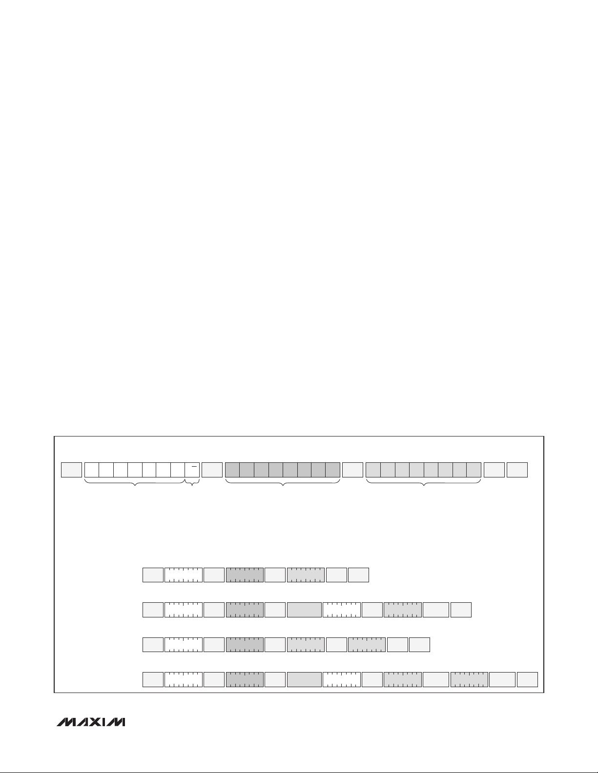
separately for permissions.
Write all, but the DS1876 hardware also writes to
these bytes/bits
Memory Addresses A0h, A2h, and B2h
There are three separate I2C addresses in the DS1876:
A0h, A2h, and B2h. A2h and B2h are used to configure
and monitor two transmitters. Transmitter 1 is accessed
MEMORY CODE A2h AND B2h REGISTERS
<C> or <_/C>
<D> or <_/D> Different memory locations are used for A2h and B2h device addresses.
<M> or <_/M>
24 _____________________________________________________________________________________
A common memory location is used for A2h and B2h device addresses. Reading or writing to these
locations is identical, regardless of using A2h or B2h addresses.
Mixture of common and different memory locations for A2h and B2h device addresses. See the individual
bytes within the row for clarification. If “M” is used on an individual byte, see the expanded bit descriptions
to determine which bits are common vs. different.
using A2h. Transmitter 2 is accessed using B2h. Many
of the registers in A2h and B2h are shared registers.
These registers can be read and written from both A2h
and B2h.
Page 25

SFP Controller with Dual LDD Interface
Lower Memory Register Map
LOWER MEMORY
ROW
(HEX)
00
08
10
18
20–40
48–50
58
60
68
70
78
ROW NAME
<1/C>
THRESHOLD
<1/C >
THRESHOLD
<1/D>
THRESHOLD
<1/D>
THRESHOLD
<1/C >
<1/D >
<1/C >
<2/M>
ADC VALUES
<0/M>
ADC VALUES
<5/D>
ALARM/WARN ALARM
<0/M>
TABLE SELECT RESERVED RESERVED RESERVED
0
1
2
3
EEPROM EE EE EE EE
EEPROM EE EE EE EE
EEPROM EE EE EE EE EE EE EE EE
0
1
<C> or <_/C> = Common, <D> or <_/D> = Different, <M> or <_/M> = Mixture of common and different.
Table 01h Register Map
ROW
(HEX)
80–F7
F8
<C> or <_/C> = Common, <D> or <_/D> = Different, <M> or <_/M> = Mixture of common and different.
Note: The ALARM ENABLE bytes (Registers F8h–FFh) can be configured to exist in Table 05h instead of here at Table 01h with
the MASK bit (Table 02h, Register 88h). If the row is configured to exist in Table 05h, these location are empty in Table 01h.
ROW NAME
<1/C>
EEPROM EE EE EE EE EE EE EE EE
<7/M>
ALARM ENABLE
<M>
WORD 0 WORD 1 WORD 2 WORD 3
BYTE 0/8 BYTE 1/9 BYTE 2/A BYTE 3/B BYTE 4/C BYTE 5/D BYTE 6/E BYTE 7/F
TEMP ALARM HI TEMP ALARM LO TEMP WARN HI TEMP WARN LO
VCC ALARM HI VCC ALARM LO VCC WARN HI VCC WARN LO
BMON ALARM HI BMON ALARM LO BMON WARN HI BMON WARN LO
PMON ALARM HI PMON ALARM LO PMON WARN HI PMON WARN LO
<C>
TEMP VALUE
RESERVED RESERVED RESERVED
3
BYTE 0/8 BYTE 1/9 BYTE 2/A BYTE 3/B BYTE 4/C BYTE 5/D BYTE 6/E BYTE 7/F
ALARM EN3RESERVED
ALARM
2
WORD 0 WORD 1 WORD 2 WORD 3
<C>
VCC VALUE
ALARM
<D>
ALARM EN1RESERVED
RESERVED WARN
1
TABLE 01h
<6/C>
<D>
BMON VALUE
RESERVED RESERVED RESERVED
3
PWE MSW
<M>
WARN EN3RESERVED RESERVED RESERVED
<6/C>
PWE LSW
<0/M>
<D>
PMON VALUE
STATUS
<3/D>
<5/D>
UPDATE
TBL SEL
DS1876
The access codes represent the factory default values of PW_ENA and PW_ENB (Table 02h, Registers C0h–C1h).
These registers also allow for custom permissions.
ACCESS
CODE
Read
Access
Write
Access
<0/_> <1/_> <2/_> <3/_> <4/_> <5/_> <6/_> <7/_> <8/_> <9/_> <10/_> <11/_>
See each
bit/byte
separately
All All All PW2 All N/A PW1 PW2 N/A PW2 All
PW2 N/A
All and
DS1876
Hardware
PW2 +
mode
bit
All All PW1 PW2 PW2 N/A PW1
______________________________________________________________________________________ 25
Page 26

SFP Controller with Dual LDD Interface
Table 02h Register Map
TABLE 02h (PW2)
ROW
(HEX)
80
DS1876
88
90
98
A0
A8
B0
B8
C0
C8
D0–FF EMPTY EMPTY EMPTY EMPTY EMPTY EMPTY EMPTY EMPTY EMPTY
ROW NAME
<0/C>
CONFIG
<8/C>
<8/C>
<8/C>
<8/C>
<8/C>
<9/C>
<8/C>
<8/C>
PWD ENABLE PW_ENA PW_ENB RESERVED RESERVED RESERVED RESERVED POLARITY TBLSELPON
<4/C>
DAC VALUES MOD2 DAC APC2 DAC MOD1 DAC APC1 DAC
0
CONFIG
1
SCALE
0
SCALE
1
OFFSET
0
OFFSET
1
PWD VALUE PW1 MSW PW1 LSW PW2 MSW PW2 LSW
THRESHOLD RESERVED HBIAS2 DAC HTXP2 DAC LTXP2 DAC RESERVED HBIAS1 DAC HTXP1 DAC LTXP1 DAC
<C> or <_/C> = Common, <D> or <_/D> = Different, <M> or <_/M> = Mixture of common and different.
*The final result must be XORed with BB40h before writing to this register.
Table 04h Register Map
WORD 0 WORD 1 WORD 2 WORD 3
BYTE 0/8 BYTE 1/9 BYTE 2/A BYTE 3/B BYTE 4/C BYTE 5/D BYTE 6/E BYTE 7/F
<8/C>
MODE
CNFGA CNFGB CNFGC DEVICE ADDRESS RANGING
INTERNAL TEMP OFFSET* VCC OFFSET RESERVED RESERVED
BMON2 OFFSET PMON2 OFFSET BMON1 OFFSET PMON1 OFFSET
<4/C>
TINDEX RESERVED RESERVED RESERVED RESERVED
RANGING
2
RESERVED VCC SCALE RESERVED RESERVED
BMON2 SCALE PMON2 SCALE BMON1 SCALE PMON1 SCALE
<10>
DEVICE ID
RSHIFT
1
<10>
2
DEVICE VER
RSHIFT
1
TABLE 04h (MODULATION LUT)
ROW
(HEX)
80–C7
C8–F7 EMPTY EMPTY EMPTY EMPTY EMPTY EMPTY EMPTY EMPTY EMPTY
F8
ROW NAME
<8/D>
LUT4 MOD MOD MOD MOD MOD MOD MOD MOD
<8/D>
MOD OFFSET
MOD OFFSET
WORD 0 WORD 1 WORD 2 WORD 3
BYTE 0/8 BYTE 1/9 BYTE 2/A BYTE 3/B BYTE 4/C BYTE 5/D BYTE 6/E BYTE 7/F
LUT
MOD OFFSET
LUT
MOD OFFSET
LUT
MOD OFFSET
LUT
MOD OFFSET
LUT
MOD OFFSET
LUT
MOD OFFSET
LUT
MOD OFFSET
LUT
<C> or <_/C> = Common, <D> or <_/D> = Different, <M> or <_/M> = Mixture of common and different.
The access codes represent the factory default values of PW_ENA and PW_ENB (Table 02h, Registers C0h–C1h).
These registers also allow for custom permissions.
ACCESS
CODE
Read
Access
Write
Access
<0/_> <1/_> <2/_> <3/_> <4/_> <5/_> <6/_> <7/_> <8/_> <9/_> <10/_> <11/_>
See each
bit/byte
separately
All All All PW2 All N/A PW1 PW2 N/A PW2 All
PW2 N/A
All and
DS1876
Hardware
PW2 +
mode
bit
All All PW1 PW2 PW2 N/A PW1
26 _____________________________________________________________________________________
Page 27

SFP Controller with Dual LDD Interface
Table 05h Register Map
TABLE 05h
ROW
(HEX)
80–F7 EMPTY EMPTY EMPTY EMPTY EMPTY EMPTY EMPTY EMPTY EMPTY
F8
ROW NAME
<7/M>
ALARM ENABLE
<M>
<C> or <_/C> = Common, <D> or <_/D> = Different, <M> or <_/M> = Mixture of common and different.
Note: Table 05h is empty by default. It can be configured to contain the alarm and warning enable bytes from Table 01h,
Registers F8h–FFh with the MASK bit enabled (Table 02h, Register 88h). In this case Table 01h is empty.
Table 06h Register Map
ROW
(HEX)
80–C7
C8–DF EMPTY EMPTY EMPTY EMPTY EMPTY EMPTY EMPTY EMPTY EMPTY
E0
E8
F0
F8
<C> or <_/C> = Common, <D> or <_/D> = Different, <M> or <_/M> = Mixture of common and different.
ROW NAME
<8/D>
LUT6 APC LUT APC LUT APC LUT APC LUT APC LUT APC LUT APC LUT APC LUT
<8/D>
HBATH HBATH LUT HBATH LUT HBATH LUT HBATH LUT HBATH LUT HBATH LUT HBATH LUT HBATH LUT
<8/D>
HTXP HTXP LUT HTXP LUT HTXP LUT HTXP LUT HTXP LUT HTXP LUT HTXP LUT HTXP LUT
<8/D>
LTXP LTXP LUT LTXP LUT LTXP LUT LTXP LUT LTXP LUT LTXP LUT LTXP LUT LTXP LUT
<8/D>
APC OFFSET
APC OFFSET
WORD 0 WORD 1 WORD 2 WORD 3
BYTE 0/8 BYTE 1/9 BYTE 2/A BYTE 3/B BYTE 4/C BYTE 5/D BYTE 6/E BYTE 7/F
ALARM EN3RESERVED
WORD 0 WORD 1 WORD 2 WORD 3
BYTE 0/8 BYTE 1/9 BYTE 2/A BYTE 3/B BYTE 4/C BYTE 5/D BYTE 6/E BYTE 7/F
APC OFFSET
LUT
LUT
<D>
ALARM EN1RESERVED
TABLE 06h (APC LUT)
APC OFFSET
LUT
APC OFFSET
LUT
<M>
WARN EN3RESERVED RESERVED RESERVED
APC OFFSET
LUT
APC OFFSET
LUT
APC OFFSET
LUT
APC OFFSET
LUT
DS1876
Auxiliary Memory A0h Register Map
AUXILIARY MEMORY (A0h)
ROW
(HEX)
00–7F
80–FF
ROW NAME
<5>
AUX EE EE EE EE EE EE EE EE EE
<5>
AUX EE EE EE EE EE EE EE EE EE
<C> or <_/C> = Common, <D> or <_/D> = Different, <M> or <_/M> = Mixture of common and different.
The access codes represent the factory default values of PW_ENA and PW_ENB (Table 02h, Registers C0h–C1h).
These registers also allow for custom permissions.
ACCESS
CODE
Read
Access
Write
Access
<0/_> <1/_> <2/_> <3/_> <4/_> <5/_> <6/_> <7/_> <8/_> <9/_> <10/_> <11/_>
See each
bit/byte
separately
PW2 N/A
______________________________________________________________________________________ 27
WORD 0 WORD 1 WORD 2 WORD 3
BYTE 0/8 BYTE 1/9 BYTE 2/A BYTE 3/B BYTE 4/C BYTE 5/D BYTE 6/E BYTE 7/F
All All All PW2 All N/A PW1 PW2 N/A PW2 All
All and
DS1876
Hardware
PW2 +
mode
bit
All All PW1 PW2 PW2 N/A PW1
Page 28

SFP Controller with Dual LDD Interface
Lower Memory Register Descriptions
Lower Memory, Register 00h–01h: TEMP ALARM HI
Lower Memory, Register 04h–05h: TEMP WARN HI
FACTORY DEFAULT 7FFFh
READ ACCESS All
DS1876
WRITE ACCESS PW2 or (PW1 and WLOWER)
A2h AND B2h MEMORY Common A2h and B2h memory location
MEMORY TYPE Nonvolatile (SEE)
00h, 04h S 2
01h, 05h 2
-1
6
-2
2
5
2
-3
2
BIT 7 BIT 0
Temperature measurement updates above this two’s complement threshold set its corresponding alarm or
warning bit. Temperature measurement updates equal to or below this threshold clear its alarm or warning bit.
Lower Memory, Register 02h–03h: TEMP ALARM LO
Lower Memory, Register 06h–07h: TEMP WARN LO
FACTORY DEFAULT 8000h
READ ACCESS All
WRITE ACCESS PW2 or (PW1 and WLOWER)
A2h AND B2h MEMORY Common A2h and B2h memory location
MEMORY TYPE Nonvolatile (SEE)
02h, 06h S 2
03h, 07h 2
-1
BIT 7 BIT 0
Temperature measurement updates below this two’s complement threshold set its corresponding alarm or
warning bit. Temperature measurement updates equal to or above this threshold clear its alarm or warning bit.
6
-2
2
5
2
-3
2
4
2
-4
2
4
2
-4
2
3
2
-5
2
3
2
-5
2
2
2
-6
2
2
2
-6
2
1
2
-7
2
1
2
-7
2
0
2
-8
2
0
2
-8
2
28 _____________________________________________________________________________________
Page 29

SFP Controller with Dual LDD Interface
Lower Memory, Register 08h–09h: VCC ALARM HI
Lower Memory, Register 0Ch–0Dh: VCC WARN HI
FACTORY DEFAULT FFFFh
READ ACCESS All
WRITE ACCESS PW2 or (PW1 and WLOWER)
A2h AND B2h MEMORY Common A2h and B2h memory location
MEMORY TYPE Nonvolatile (SEE)
DS1876
08h, 0Ch 2
09h, 0Dh 2
15
7
14
2
6
2
13
2
5
2
BIT 7 BIT 0
Voltage measurement updates above this unsigned threshold set its corresponding alarm or warning bit.
Voltage measurements equal to or below this threshold clear its alarm or warning bit.
Lower Memory, Register 0Ah–0Bh: VCC ALARM LO
Lower Memory, Register 0Eh–0Fh: VCC WARN LO
FACTORY DEFAULT 0000h
READ ACCESS All
WRITE ACCESS PW2 or (PW1 and WLOWER)
A2h AND B2h MEMORY Common A2h and B2h memory location
MEMORY TYPE Nonvolatile (SEE)
0Ah, 0Eh 2
0Bh, 0Fh 2
BIT 7 BIT 0
Voltage measurement updates below this unsigned threshold set its corresponding alarm or warning bit. Voltage
measurements equal to or above this threshold clear its alarm or warning bit.
15
7
14
2
6
2
13
2
5
2
12
2
4
2
12
2
4
2
11
2
3
2
11
2
3
2
10
2
2
2
10
2
2
2
9
2
1
2
9
2
1
2
8
2
0
2
8
2
0
2
______________________________________________________________________________________ 29
Page 30

SFP Controller with Dual LDD Interface
Lower Memory, Register 10h–11h: BMON ALARM HI
Lower Memory, Register 14h–15h: BMON WARN HI
Lower Memory, Register 18h–19h: PMON ALARM HI
Lower Memory, Register 1Ch–1Dh: PMON WARN HI
DS1876
FACTORY DEFAULT FFFFh
READ ACCESS All
WRITE ACCESS PW2 or (PW1 and WLOWER)
A2h AND B2h MEMORY Different A2h and B2h memory locations
MEMORY TYPE Nonvolatile (SEE)
10h, 14h,
18h, 1Ch
11h, 15h,
19h, 1Dh
15
2
7
2
14
2
6
2
13
2
5
2
BIT 7 BIT 0
Voltage measurement updates above this unsigned threshold set its corresponding alarm or warning bit.
Voltage measurements equal to or below this threshold clear its alarm or warning bit.
Lower Memory, Register 12h–13h: BMON ALARM LO
Lower Memory, Register 16h–17h: BMON WARN LO
Lower Memory, Register 1Ah–1Bh: PMON ALARM LO
Lower Memory, Register 1Eh–1Fh: PMON WARN LO
FACTORY DEFAULT 0000h
READ ACCESS All
WRITE ACCESS PW2 or (PW1 and WLOWER)
A2h AND B2h MEMORY Different A2h and B2h memory locations
MEMORY TYPE Nonvolatile (SEE)
12
2
4
2
11
2
3
2
10
2
2
2
9
2
1
2
8
2
0
2
12h, 16h,
1Ah, 1Eh
13h, 17h,
1Bh, 1Fh
15
2
7
2
14
2
6
2
13
2
5
2
12
2
4
2
11
2
3
2
10
2
2
2
2
2
BIT 7 BIT 0
Voltage measurement updates below this unsigned threshold set its corresponding alarm or warning bit. Voltage
measurements equal to or above this threshold clear its alarm or warning bit.
30 _____________________________________________________________________________________
9
1
8
2
0
2
Page 31

SFP Controller with Dual LDD Interface
Lower Memory, Register 20h–47h: EE
FACTORY DEFAULT 00h
READ ACCESS All
WRITE ACCESS PW2 or (PW1 and WLOWER)
A2h AND B2h MEMORY Common A2h and B2h memory location
MEMORY TYPE Nonvolatile (EE)
20h–47h EE EE EE EE EE EE EE EE
BIT 7 BIT 0
PW2 level access-controlled EEPROM.
Lower Memory, Register 48h–57h: EE
FACTORY DEFAULT 00h
READ ACCESS All
WRITE ACCESS PW2 or (PW1 and WLOWER)
A2h AND B2h MEMORY Different A2h and B2h memory locations
MEMORY TYPE Nonvolatile (EE)
DS1876
48h–57h EE EE EE EE EE EE EE EE
BIT 7 BIT 0
PW2 level access-controlled EEPROM.
Lower Memory, Register 58h–5Fh: EE
FACTORY DEFAULT 00h
READ ACCESS All
WRITE ACCESS PW2 or (PW1 and WLOWER)
A2h AND B2h MEMORY Common A2h and B2h memory location
MEMORY TYPE Nonvolatile (EE)
58h–5Fh EE EE EE EE EE EE EE EE
BIT 7 BIT 0
PW2 level access-controlled EEPROM.
______________________________________________________________________________________ 31
Page 32

SFP Controller with Dual LDD Interface
Lower Memory, Register 60h–61h: TEMP VALUE
FACTORY DEFAULT 0000h
READ ACCESS All
WRITE ACCESS N/A
A2h AND B2h MEMORY Common A2h and B2h memory location
DS1876
MEMORY TYPE Volatile
60h S 2
61h 2
-1
6
-2
2
5
2
-3
2
BIT 7 BIT 0
Signed two’s complement direct-to-temperature measurement.
Lower Memory, Register 62h–63h: VCC VALUE
POWER-ON VALUE 0000h
READ ACCESS All
WRITE ACCESS N/A
A2h AND B2h MEMORY Common A2h and B2h memory location
MEMORY TYPE Volatile
62h 2
63h 2
15
7
BIT 7 BIT 0
Left-justified unsigned voltage measurement.
14
2
6
2
13
2
5
2
4
2
-4
2
12
2
4
2
3
2
-5
2
11
2
3
2
2
2
-6
2
10
2
2
2
1
2
-7
2
9
2
1
2
0
2
-8
2
8
2
0
2
32 _____________________________________________________________________________________
Page 33

SFP Controller with Dual LDD Interface
Lower Memory, Register 64h–65h: BMON VALUE
Lower Memory, Register 66h–67h: PMON VALUE
POWER-ON VALUE 0000h
READ ACCESS All
WRITE ACCESS N/A
A2h AND B2h MEMORY Different A2h and B2h memory locations
MEMORY TYPE Volatile
DS1876
64h, 66h 2
65h, 67h 2
BIT 7 BIT 0
Left-justified unsigned voltage measurement.
15
7
14
2
6
2
13
2
5
2
12
2
4
2
11
2
3
2
10
2
2
2
9
2
1
2
Lower Memory, Register 68h–6Dh: RESERVED
POWER-ON VALUE
READ ACCESS N/A
WRITE ACCESS N/A
A2h AND B2h MEMORY N/A
MEMORY TYPE N/A
68h, 6Dh 0 0 0 0 0 0 0 0
BIT 7 BIT 0
These registers are reserved. The value when read is 00h.
8
2
0
2
______________________________________________________________________________________ 33
Page 34

SFP Controller with Dual LDD Interface
Lower Memory, Register 6Eh: STATUS
POWER-ON VALUE X0XX 0XXXb
READ ACCESS All
WRITE ACCESS See below
A2h AND B2h MEMORY Mixture of common memory locations and different memory locations (see below)
DS1876
Write Access N/A All N/A All All N/A N/A N/A
MEMORY TYPE Volatile
6Eh
<D>
TXDS
BIT 7 BIT 0
BIT 7
BIT 6
BIT 5
BIT 4
BIT 3
BIT 2
BIT 1
BIT 0
<D>
TXDC
TXDS1 [A2h]: TXD1 status bit. Reflects the logic state of the TXD1 pin (read-only).
0 = TXD1 pin is logic-low.
1 = TXD1 pin is logic-high.
TXDS2 [B2h]: TXD2 status bit. Reflects the logic state of the TXD2 pin (read-only).
0 = TXD2 pin is logic-low.
1 = TXD2 pin is logic-high.
TXDC1 [A2h]: TXD1 software control bit. This bit allows for software control that is identical to the
TXD1 pin. See the DACs as a Function of Transmit Disable (TXD1, TXD2) section for further information. Its value is wire-ORed with the logic value of the TXD1 pin (writable by all users).
0 = (default)
1 = Forces the device into a TXD1 state regardless of the value of the TXD1 pin.
TXDC2 [B2h]: TXD2 software control bit. This bit allows for software control that is identical to the
TXD2 pin. See the DACs as a Function of Transmit Disable (TXD1, TXD2) section for further information. Its value is wire-ORed with the logic value of the TXD2 pin (writable by all users).
0 = (default)
1 = Forces the device into a TXD2 state regardless of the value of the TXD2 pin.
IN1S [A2h or B2h]: IN1 status bit. Reflects the logic state of the IN1 pin (read-only).
0 = IN1 pin is logic-low.
1 = IN1 pin is logic-high.
RSELS [A2h or B2h]: RSEL status bit. Reflects the logic state of the RSEL pin (read-only).
0 = RSEL pin is logic-low.
1 = RSEL pin is logic-high.
RSELC [A2h or B2h]: RSEL software control bit. This bit allows for software control that is identical to the RSEL pin. Its value is wire-ORed with the logic value of the RSEL pin to create the
RSELOUT pin’s logic value (writable by all users).
0 = (default)
1 = Forces the device into a RSEL state regardless of the value of the RSEL pin.
TXFS1 [A2h]: Reflects state of the TXF1 pin (read-only).
0 = TXF1 pin is low.
1 = TXF1 pin is high.
TXFS2 [B2h]: Reflects the state of the TXF2 pin (read-only).
0 = TXF2 pin is low.
1 = TXF2 pin is high.
RAM1 [A2h]: Volatile memory location.
RAM2 [B2h]: Volatile memory location.
RDYB [A2h or B2h]: Ready bar.
0 = V
CC
1 = VCC is below POA and/or too low to communicate over the I2C bus.
<C>
IN1S
is above POA.
<C>
RSELS
<C>
RSELC
<D>
TXFS
<D>
RAM
<C>
RDYB
34 _____________________________________________________________________________________
Page 35

SFP Controller with Dual LDD Interface
Lower Memory, Register 6Fh: UPDATE
POWER-ON VALUE 00h
READ ACCESS All
WRITE ACCESS All and DS1876 hardware
A2h AND B2h MEMORY Different A2h and B2h memory locations
MEMORY TYPE Volatile
DS1876
6Fh
TEMP
RDY
BIT 7 BIT 0
BITS 7:4
BITS 3:0 RESERVED
VCC RDY
TEMP RDY, VCC RDY, BMON RDY, PMON RDY: Update of completed conversions. At power-on,
these bits are cleared and are set as each conversion is completed. These bits can be cleared so
that a completion of a new conversion is verified.
BMON
RDY
PMON
RDY
RESERVED RESERVED RESERVED RESERVED
______________________________________________________________________________________ 35
Page 36

SFP Controller with Dual LDD Interface
Lower Memory, Register 70h: ALARM
POWER-ON VALUE 10h
READ ACCESS All
WRITE ACCESS N/A
A2h AND B2h MEMORY Different A2h and B2h memory locations
DS1876
MEMORY TYPE Volatile
70h TEMP HI TEMP LO VCC HI VCC LO BMON HI BMON LO PMON HI PMON LO
BIT 7 BIT 0
TEMP HI: High alarm status for temperature measurement.
BIT 7
BIT 6
BIT 5
BIT 4
BIT 3
BIT 2
BIT 1
BIT 0
0 = (default) Last measurement was equal to or below threshold setting.
1 = Last measurement was above threshold setting.
TEMP LO: Low alarm status for temperature measurement.
0 = (default) Last measurement was equal to or above threshold setting.
1 = Last measurement was below threshold setting.
VCC HI: High alarm status for VCC measurement.
0 = (default) Last measurement was equal to or below threshold setting.
1 = Last measurement was above threshold setting.
VCC LO: Low alarm status for VCC measurement. This bit is set when the VCC supply is below
the POA trip point value. It clears itself when a VCC measurement is completed and the value is
above the low threshold.
0 = Last measurement was equal to or above threshold setting.
1 = (default) Last measurement was below threshold setting.
BMON HI: High alarm status for BMON measurement.
0 = (default) Last measurement was equal to or below threshold setting.
1 = Last measurement was above threshold setting.
BMON LO: Low alarm status for BMON measurement.
0 = (default) Last measurement was equal to or above threshold setting.
1 = Last measurement was below threshold setting.
PMON HI: High alarm status for PMON measurement.
0 = (default) Last measurement was equal to or below threshold setting.
1 = Last measurement was above threshold setting.
PMON LO: Low alarm status for PMON measurement.
0 = (default) Last measurement was equal to or above threshold setting.
1 = Last measurement was below threshold setting.
3
36 _____________________________________________________________________________________
Page 37

SFP Controller with Dual LDD Interface
Lower Memory, Register 71h: ALARM
POWER-ON VALUE 00h
READ ACCESS All
WRITE ACCESS N/A
A2h AND B2h MEMORY Mixed A2h and B2h memory locations
MEMORY TYPE Volatile
DS1876
2
71h RESERVED RESERVED RESERVED RESERVED RESERVED
BIT 7 BIT 0
BITS 7:3 RESERVED
TXFOUTS: TXFOUT status. Indicates the state the open-drain output is attempting to achieve.
BIT 2
BIT 1
BIT 0
Lower Memory, Register 72h: ALARM
POWER-ON VALUE 00h
READ ACCESS All
WRITE ACCESS N/A
A2h AND B2h MEMORY Different A2h and B2h memory locations
MEMORY TYPE Volatile
72h RESERVED RESERVED RESERVED RESERVED HBAL RESERVED TXP HI TXP LO
BIT 7 BIT 0
0 = TXFOUT is pulling low.
1 = TXFOUT is high impedance.
FETG: Status of internal signal FETG. The FETG signal is part of the internal shutdown logic.
0 = (default) FETG is low.
1 = FETG is high.
TXFINT: TXF interrupt. This bit is the wire-ORed logic of all alarms and warnings wire-ANDed with
their corresponding enable bits, plus the wire-ORed logic of HBAL, TXP HI, and TXP LO. The enable
bits are found in Table 01h/05h, Registers F8h–FFh.
1
<C>
TXFOUTS
<D>
FETG
<D>
TXFINT
BITS 7:4, 2 RESERVED
HBAL: High bias alarm status; fast comparison. A TXD event clears this alarm.
BIT 3
BIT 1
BIT 0
______________________________________________________________________________________ 37
0 = (default) Last comparison was below threshold setting.
1 = Last comparison was above threshold setting.
TXP HI: High alarm status TXP; fast comparison. A TXD event clears this alarm.
0 = (default) Last comparison was below threshold setting.
1 = Last comparison was above threshold setting.
TXP LO: Low alarm status TXP; fast comparison. A TXD event clears this alarm.
0 = (default) Last comparison was above threshold setting.
1 = Last comparison was below threshold setting.
Page 38

SFP Controller with Dual LDD Interface
Lower Memory, Register 73h: RESERVED
POWER-ON VALUE
READ ACCESS N/A
WRITE ACCESS N/A
A2h AND B2h MEMORY N/A
DS1876
MEMORY TYPE N/A
This register is reserved.
Lower Memory, Register 74h: WARN
POWER-ON VALUE 10h
READ ACCESS All
WRITE ACCESS N/A
A2h AND B2h MEMORY Different A2h and B2h memory locations
MEMORY TYPE Volatile
74h TEMP HI TEMP LO VCC HI VCC LO BMON HI BMON LO PMON HI PMON LO
BIT 7 BIT 0
TEMP HI: High warning status for temperature measurement.
BIT 7
BIT 6
BIT 5
BIT 4
BIT 3
BIT 2
BIT 1
BIT 0
0 = (default) Last measurement was equal to or below threshold setting.
1 = Last measurement was above threshold setting.
TEMP LO: Low warning status for temperature measurement.
0 = (default) Last measurement was equal to or above threshold setting.
1 = Last measurement was below threshold setting.
VCC HI: High warning status for VCC measurement.
0 = (default) Last measurement was equal to or below threshold setting.
1 = Last measurement was above threshold setting.
VCC LO: Low warning status for VCC measurement. This bit is set when the VCC supply is below
the POA trip-point value. It clears itself when a VCC measurement is completed and the value is
above the low threshold.
0 = Last measurement was equal to or above threshold setting.
1 = (default) Last measurement was below threshold setting.
BMON HI: High warning status for BMON measurement.
0 = (default) Last measurement was equal to or below threshold setting.
1 = Last measurement was above threshold setting.
BMON LO: Low warning status for BMON measurement.
0 = (default) Last measurement was equal to or above threshold setting.
1 = Last measurement was below threshold setting.
PMON HI: High warning status for PMON measurement.
0 = (default) Last measurement was equal to or below threshold setting.
1 = Last measurement was above threshold setting.
PMON LO: Low warning status for PMON measurement.
0 = (default) Last measurement was equal to or above threshold setting.
1 = Last measurement was below threshold setting.
3
38 _____________________________________________________________________________________
Page 39

SFP Controller with Dual LDD Interface
Lower Memory, Registers 75h–7Ah: RESERVED MEMORY
POWER-ON VALUE
READ ACCESS N/A
WRITE ACCESS N/A
A2h AND B2h MEMORY N/A
MEMORY TYPE N/A
These registers are reserved. The value when read is 00h.
Lower Memory, Registers 7Bh–7Eh: PASSWORD ENTRY (PWE)
POWER-ON VALUE FFFF FFFFh
READ ACCESS N/A
WRITE ACCESS All
A2h AND B2h MEMORY Common A2h and B2h memory location
MEMORY TYPE Volatile
DS1876
7Bh 2
7Ch 2
7Dh 2
7Eh 2
31
23
15
7
30
2
22
2
14
2
6
2
29
2
21
2
13
2
5
2
28
2
20
2
12
2
4
2
27
2
19
2
11
2
3
2
26
2
18
2
10
2
2
2
25
2
17
2
9
2
1
2
BIT 7 BIT 0
There are two passwords for the DS1876. Each password is 4 bytes long. The lower level password (PW1) has
all the access of a normal user plus those made available with PW1. The higher level password (PW2) has all the
access of PW1 plus those made available with PW2. The values of the passwords reside in EEPROM inside PW2
memory. At power-up, all PWE bits are set to 1. All reads at this location are 0.
24
2
16
2
8
2
0
2
______________________________________________________________________________________ 39
Page 40

SFP Controller with Dual LDD Interface
Lower Memory, Register 7Fh: TABLE SELECT (TBL SEL)
POWER-ON VALUE TBLSELPON (Table 02h, Register C7h)
READ ACCESS All
WRITE ACCESS All
A2h AND B2h MEMORY Different A2h and B2h memory locations
DS1876
MEMORY TYPE Volatile
7Fh 2
7
BIT 7 BIT 0
The upper memory tables of the DS1876 are accessible by writing the desired table value in this register. The
power-on value of this register is defined by the value written to TBLSELPON (Table 02h, Register C7h).
6
2
5
2
4
2
3
2
2
2
1
2
Table 01h Register Descriptions
Table 01h, Register 80h–F7h: EEPROM
POWER-ON VALUE 00h
READ ACCESS PW2 or (PW1 and RWTBL1A) or (PW1 and RTBL1A)
WRITE ACCESS PW2 or (PW1 and RWTBL1A)
A2h AND B2h MEMORY Common A2h and B2h memory location
MEMORY TYPE Nonvolatile (EE)
80h–F7h EE EE EE EE EE EE EE EE
BIT 7 BIT 0
EEPROM for PW1 and/or PW2 level access.
0
2
40 _____________________________________________________________________________________
Page 41

SFP Controller with Dual LDD Interface
Table 01h, Register F8h: ALARM EN
POWER-ON VALUE 00h
READ ACCESS PW2 or (PW1 and RWTBL1C) or (PW1 and RTBL1C)
WRITE ACCESS PW2 or (PW1 and RWTBL1C)
A2h AND B2h MEMORY
MEMORY TYPE Nonvolatile (SEE)
DS1876
3
Mixture of common memory locations and different memory locations (see the
descriptions below)
<C>
F8h
TEMP HI
BIT 7 BIT 0
Layout is identical to ALARM3 in Lower Memory, Register 70h. Enables alarms to create TXFINT (Lower Memory,
Register 71h) logic. The MASK bit (Table 02h, Register 88h) determines whether this memory exists in Table 01h or 05h.
BIT 7
BIT 6
BIT 5
BIT 4
BIT 3
BIT 2
BIT 1
BIT 0
<C>
TEMP LO
TEMP HI [A2h or B2h]:
0 = Disables interrupt from TEMP HI alarm.
1 = Enables interrupt from TEMP HI alarm.
TEMP LO [A2h or B2h]:
0 = Disables interrupt from TEMP LO alarm.
1 = Enables interrupt from TEMP LO alarm.
VCC HI [A2h or B2h]:
0 = Disables interrupt from VCC HI alarm.
1 = Enables interrupt from VCC HI alarm.
VCC LO [A2h or B2h]:
0 = Disables interrupt from VCC LO alarm.
1 = Enables interrupt from VCC LO alarm.
BMON1 HI [A2h]:
0 = Disables interrupt from BMON1 HI alarm.
1 = Enables interrupt from BMON1 HI alarm.
BMON2 HI [B2h]:
0 = Disables interrupt from BMON2 HI alarm.
1 = Enables interrupt from BMON2 HI alarm.
BMON1 LO [A2h]:
0 = Disables interrupt from BMON1 LO alarm.
1 = Enables interrupt from BMON1 LO alarm.
BMON2 LO [B2h]:
0 = Disables interrupt from BMON2 LO alarm.
1 = Enables interrupt from BMON2 LO alarm.
PMON1 HI [A2h]:
0 = Disables interrupt from PMON1 HI alarm.
1 = Enables interrupt from PMON1 HI alarm.
PMON2 HI [B2h]:
0 = Disables interrupt from PMON2 HI alarm.
1 = Enables interrupt from PMON2 HI alarm.
PMON1 LO [A2h]:
0 = Disables interrupt from PMON1 LO alarm.
1 = Enables interrupt from PMON1 LO alarm.
PMON2 LO [B2h]:
0 = Disables interrupt from PMON2 LO alarm.
1 = Enables interrupt from PMON2 LO alarm.
<C>
VCC HI
<C>
VCC LO
<D>
BMON HI
<D>
BMON LO
<D>
PMON HI
<D>
PMON LO
______________________________________________________________________________________ 41
Page 42

SFP Controller with Dual LDD Interface
Table 01h, Register F9h: RESERVED
POWER-ON VALUE
READ ACCESS N/A
WRITE ACCESS N/A
A2h AND B2h MEMORY N/A
DS1876
MEMORY TYPE N/A
This register is reserved.
Table 01h, Register FAh: ALARM EN
POWER-ON VALUE 00h
READ ACCESS PW2 or (PW1 and RWTBL1C) or (PW1 and RTBL1C)
WRITE ACCESS PW2 or (PW1 and RWTBL1C)
A2h AND B2h MEMORY Different A2h and B2h memory locations
MEMORY TYPE Nonvolatile (SEE)
FAh RESERVED RESERVED RESERVED RESERVED HBAL RESERVED TXP HI TXP LO
BIT 7 BIT 0
Layout is identical to ALARM1 in Lower Memory, Register 72h. Enables alarms to create internal signal FETG (see
Figure 9). The MASK bit (Table 02h, Register 88h) determines whether this memory exists in Table 01h or 05h.
BITS 7:4, 2 RESERVED
HBAL: Enables alarm to create internal signal FETG.
BIT 3
BIT 1
BIT 0
0 = Disables interrupt from HBAL alarm.
1 = Enables interrupt from HBAL alarm.
TXP HI: Enables alarm to create internal signal FETG.
0 = Disables interrupt from TXP HI alarm.
1 = Enables interrupt from TXP HI alarm.
TXP LO: Enables alarm to create internal signal FETG.
0 = Disables interrupt from TXP LO alarm.
1 = Enables interrupt from TXP LO alarm.
1
Table 01h, Register FBh: RESERVED
POWER-ON VALUE
READ ACCESS N/A
WRITE ACCESS N/A
A2h AND B2h MEMORY N/A
MEMORY TYPE N/A
This register is reserved.
42 _____________________________________________________________________________________
Page 43

SFP Controller with Dual LDD Interface
Table 01h, Register FCh: WARN EN
POWER-ON VALUE 00h
READ ACCESS PW2 or (PW1 and RWTBL1C) or (PW1 and RTBL1C)
WRITE ACCESS PW2 or (PW1 and RWTBL1C)
A2h AND B2h MEMORY
MEMORY TYPE Nonvolatile (SEE)
DS1876
3
Mixture of common memory locations and different memory locations (see the bit
descriptions)
<C>
FCh
TEMP HI
BIT 7 BIT 0
Layout is identical to WARN3 in Lower Memory, Register 74h. Enables warnings to create TXFINT (Lower Memory,
Register 71h) logic. The MASK bit (Table 02h, Register 88h) determines whether this memory exists in Table 01h or 05h.
BIT 7
BIT 6
BIT 5
BIT 4
BIT 3
BIT 2
BIT 1
BIT 0
<C>
TEMP LO
TEMP HI [A2h or B2h]:
0 = Disables interrupt from TEMP HI warning.
1 = Enables interrupt from TEMP HI warning.
TEMP LO [A2h or B2h]:
0 = Disables interrupt from TEMP LO warning.
1 = Enables interrupt from TEMP LO warning.
VCC HI [A2h or B2h]:
0 = Disables interrupt from VCC HI warning.
1 = Enables interrupt from VCC HI warning.
VCC LO [A2h or B2h]:
0 = Disables interrupt from VCC LO warning.
1 = Enables interrupt from VCC LO warning.
BMON1 HI [A2h]:
0 = Disables interrupt from BMON1 HI warning.
1 = Enables interrupt from BMON1 HI warning.
BMON1 HI [B2h]:
0 = Disables interrupt from BMON2 HI warning.
1 = Enables interrupt from BMON2 HI warning.
BMON1 LO [A2h]:
0 = Disables interrupt from BMON1 LO warning.
1 = Enables interrupt from BMON1 LO warning.
BMON2 LO [B2h]:
0 = Disables interrupt from BMON2 LO warning.
1 = Enables interrupt from BMON2 LO warning.
PMON1 HI [A2h]:
0 = Disables interrupt from PMON1 HI warning.
1 = Enables interrupt from PMON1 HI warning.
PMON2 HI [B2h]:
0 = Disables interrupt from PMON2 HI warning.
1 = Enables interrupt from PMON2 HI warning.
PMON1 LO [A2h]:
0 = Disables interrupt from PMON1 LO warning.
1 = Enables interrupt from PMON1 LO warning.
PMON2 LO [B2h]:
0 = Disables interrupt from PMON2 LO warning.
1 = Enables interrupt from PMON2 LO warning.
<C>
VCC HI
<C>
VCC LO
<D>
BMON HI
<D>
BMON LO
<D>
PMON HI
<D>
PMON LO
______________________________________________________________________________________ 43
Page 44

SFP Controller with Dual LDD Interface
Table 01h, Register FDh–FFh: RESERVED
POWER-ON VALUE
READ ACCESS N/A
WRITE ACCESS N/A
A2h AND B2h MEMORY N/A
DS1876
Table 02h, Register 80h: MODE
MEMORY TYPE N/A
These registers are reserved.
Table 02h Register Descriptions
POWER-ON VALUE 7Fh
READ ACCESS PW2 or (PW1 and RWTBL2) or (PW1 and RTBL2)
WRITE ACCESS PW2 or (PW1 and RWTBL2)
A2h AND B2h MEMORY Common A2h and B2h memory location
MEMORY TYPE Volatile
80h SEEB MOD2EN QT2EN APC2EN AEN MOD1EN QT1EN APC1EN
BIT 7 BIT 0
BIT 7
BIT 6
BIT 5
BIT 4
BIT 3
SEEB:
0 = (default) Enables EEPROM writes to SEE bytes.
1 = Disables EEPROM writes to SEE bytes during configuration, so that the configuration of the
part is not delayed by the EE cycle time. Once the values are known, write this bit to a 0 and write
the SEE locations again for data to be written to the EEPROM.
MOD2EN:
0 = MOD2 DAC is writable by the user and the LUT recalls are disabled. This allows the user to
interactively test their modules by writing the values for MOD2. The output is updated with the new
value at the end of the write cycle. The I2C STOP condition is the end of the write cycle.
1 = (default) Enables automatic control of the LUT for MOD2 DAC.
QT2EN:
0 = QTs (HBIAS, TXP HI, TXP LO) for transmitter 2 are writable by the user and the LUT recalls are
disabled. This allows the user to interactively test their modules by writing to the QT thresholds.
The thresholds are updated with the new values at the end of the write cycle. The I2C STOP
condition is the end of the write cycle.
1 = (default) Enables automatic control of the LUT QTs for transmitter 2.
APC2EN:
0 = APC2 DAC is writable by the user and the LUT recalls are disabled. This allows the user to
interactively test their modules by writing the values for APC2. The output is updated with the new
value at the end of the write cycle. The I2C STOP condition is the end of the write cycle.
1 = (default) Enables automatic control of the LUT for APC2 DAC.
AEN:
0 = The temperature-calculated index value TINDEX is writable by the user and the updates
of calculated indexes are disabled. This allows the user to interactively test their modules by
controlling the indexing for the LUTs. The recalled values from the LUTs appear in the DAC
registers after the next completion of a temperature conversion.
1 = (default) The temperature-calculated index value TINDEX is used to control the LUTs.
44 _____________________________________________________________________________________
Page 45
SFP Controller with Dual LDD Interface
Temp_Value 40 C
TINDEX 80h
2 C
+ °
= +
°
Table 02h, Register 80h: MODE (continued)
MOD1EN:
0 = MOD1 DAC is writable by the user and the LUT recalls are disabled. This allows the user to
BIT 2
BIT 1
BIT 0
Table 02h, Register 81h: TEMPERATURE INDEX (TINDEX)
FACTORY DEFAULT 00h
READ ACCESS PW2 or (PW1 and RWTBL2) or (PW1 and RTBL2)
WRITE ACCESS (PW2 and AEN = 0) or (PW1 and RWTBL2 and AEN = 0)
A2h AND B2h MEMORY Common A2h and B2h memory location
MEMORY TYPE Volatile
interactively test their modules by writing the values for MOD1. The output is updated with the new
value at the end of the write cycle. The I2C STOP condition is the end of the write cycle.
1 = (default) Enables automatic control of the LUT for MOD1 DAC.
QT1EN:
0 = QTs (HBIAS, TXP HI, TXP LO) for transmitter 1 are writable by the user and the LUT recalls are
disabled. This allows the user to interactively test their modules by writing to the QT thresholds.
The thresholds are updated with the new values at the end of the write cycle. The I2C STOP
condition is the end of the write cycle.
1 = (default) Enables automatic control of the LUT QTs for transmitter 1.
APC1EN:
0 = APC1 DAC is writable by the user and the LUT recalls are disabled. This allows the user to
interactively test their modules by writing the values for APC1. The output is updated with the new
value at the end of the write cycle. The I2C STOP condition is the end of the write cycle.
1 = (default) Enables automatic control of the LUT for APC1 DAC.
DS1876
81h 2
7
BIT 7 BIT 0
Holds the calculated index based on the temperature measurement. This index is used for the address during lookup
of Tables 04h and 06h. Temperature measurements below -40NC or above +102NC are clamped to 80h and C7h,
respectively. The calculation of TINDEX is as follows:
For the temperature-indexed LUTs (2NC), the index used during the lookup function for each table is as follows:
Table 04h (MOD) 1 TINDEX
Table 06h (APC) 1 TINDEX
For the 8-position LUT tables, the following table shows the lookup function:
TINDEX 1000_0xxx 1001_0xxx 1001_1xxx 1010_0xxx 1010_1xxx 1011_0xxx 1011_1xxx 11xx_xxxx
BYTE F8 F9 FA FB FC FD FE FF
TEMP (NC)
______________________________________________________________________________________ 45
6
2
< -8 -8 to +8 +8 to +24 +24 to +40 +40 to +56 +56 to +72 +72 to +88
5
2
TINDEX
6
TINDEX
6
5
5
4
2
TINDEX
TINDEX
3
2
TINDEX
4
TINDEX
4
3
3
2
2
TINDEX
TINDEX
1
2
TINDEX
2
2
TINDEX
1
1
0
2
TINDEX
TINDEX
R 88
0
0
Page 46

SFP Controller with Dual LDD Interface
Table 02h, Register 82h–85h: RESERVED
FACTORY DEFAULT
READ ACCESS N/A
WRITE ACCESS N/A
A2h AND B2h MEMORY N/A
DS1876
Table 02h, Register 86h: DEVICE ID
MEMORY TYPE N/A
These registers are reserved.
FACTORY DEFAULT 76h
READ ACCESS PW2 or (PW1 and RWTBL2) or (PW1 and RTBL2)
WRITE ACCESS N/A
MEMORY TYPE ROM
86h 0 1 1 1 0 1 1 0
BIT 7 BIT 0
Hardwired connections to show the device ID.
Table 02h, Register 87h: DEVICE VER
FACTORY DEFAULT DEVICE VERSION
READ ACCESS PW2 or (PW1 and RWTBL2) or (PW1 and RTBL2)
WRITE ACCESS N/A
MEMORY TYPE ROM
87h DEVICE VERSION
BIT 7 BIT 0
Hardwired connections to show the device version.
46 _____________________________________________________________________________________
Page 47

SFP Controller with Dual LDD Interface
Table 02h, Register 88h: CNFGA
FACTORY DEFAULT C0h
READ ACCESS PW2 or (PW1 and RWTBL2) or (PW1 and RTBL2)
WRITE ACCESS PW2 or (PW1 and RWTBL2)
A2h AND B2h MEMORY Common A2h and B2h memory location
MEMORY TYPE Nonvolatile (SEE)
88h QTHEXT2 QTHEXT1 RESERVED ASEL MASK INVRSOUT INVTXFOUT2 INVTXFOUT1
BIT 7 BIT 0
QTHEXT2: QT high extension for transmitter 2.
BIT 7
BIT 6
BIT 5 RESERVED
BIT 4
0 = Disabled. TXP HI and HBIAS QT alarms of transmitter 2 immediately create FETG.
1 = (default) Enabled. TXP HI and HBIAS QT alarms of transmitter 2 do not create FETG until the
timeout of the TXD
QTHEXT1: QT high extension for transmitter 1.
0 = Disabled. TXP HI and HBIAS QT alarms of transmitter 1 immediately create FETG.
1 = (default) Enabled. TXP HI and HBIAS QT alarms of transmitter 1 do not create FETG until the
timeout of the TXD
ASEL: Address select.
0 = (default) Device address is A2h for transmitter 1 and B2h for transmitter 2.
1 = The DEVICE ADDRESS register (Table 02h, Register 8Bh) is used to determine the main device
address.
time interval.
EXT
time interval.
EXT
DS1876
BIT 3
BIT 2
BIT 1
BIT 0
MASK:
0 = (default) Alarm-enable row exists at Table 01h, Registers F8h–FFh. Table 05h, Registers F8h–
FFh are empty.
1 = Alarm-enable row exists at Table 05h, Registers F8h–FFh. Table 01h, Registers F8h–FFh are
empty.
INVRSOUT: Allow for inversion of the RSELOUT pin (see Figure 10).
0 = (default) RSELOUT is not inverted.
1 = RSELOUT is inverted.
INVTXFOUT2: Allow for inversion of signal driven by the TXF2 input pin.
0 = (default) TXF2 signal is not inverted.
1 = TXF2 signal is inverted.
INVTXFOUT1: Allow for inversion of signal driven by the TXF1 input pin.
0 = (default) TXF1 signal is not inverted.
1 = TXF1 signal is inverted.
______________________________________________________________________________________ 47
Page 48

SFP Controller with Dual LDD Interface
Table 02h, Register 89h: CNFGB
FACTORY DEFAULT 00h
READ ACCESS PW2 or (PW1 and RWTBL2) or (PW1 and RTBL2)
WRITE ACCESS PW2 or (PW1 and RWTBL2)
A2h AND B2h MEMORY Common A2h and B2h memory location
DS1876
MEMORY TYPE Nonvolatile (SEE)
89h IN1C INVOUT1 ALATCH2 QTLATCH2 WLATCH2 ALATCH1 QTLATCH1 WLATCH1
BIT 7 BIT 0
IN1C: IN1 software control bit (see Figure 10).
BIT 7
BIT 6
BIT 5
0 = IN1 pin’s logic controls OUT1 pin.
1 = OUT1 is active (bit 6 defines the polarity).
INVOUT1: Inverts the active state for OUT1 (see Figure 10).
0 = Noninverted.
1 = Inverted.
ALATCH2: ADC alarm’s comparison latch for transmitter 2. Latches alarms in Lower Memory,
Registers 70h–71h.
0 = ADC alarm and flags reflect the status of the last comparison.
1 = ADC alarm flags remain set.
BIT 4
BIT 3
BIT 2
BIT 1
BIT 0
QTLATCH2: QT’s comparison latch for transmitter 2. Latches QT alarms in Lower Memory,
Registers 72h–73h and 76h.
0 = QT alarm and warning flags reflect the status of the last comparison.
1 = QT alarm and warning flags remain set.
WLATCH2: ADC warning’s comparison latch for transmitter 2. Latches warnings in Lower Memory,
Registers 74h–75h.
0 = ADC warning flags reflect the status of the last comparison.
1 = ADC warning flags remain set.
ALATCH1: ADC alarm’s comparison latch for transmitter 1. Latches alarms in Lower Memory,
Registers 70h–71h.
0 = ADC alarm and flags reflect the status of the last comparison.
1 = ADC alarm flags remain set.
QTLATCH1: QT’s comparison latch for transmitter 1. Latches QT alarms in Lower Memory,
Registers 72h–73h and 76h.
0 = QT alarm and warning flags reflect the status of the last comparison.
1 = QT alarm and warning flags remain set.
WLATCH1: ADC warning’s comparison latch for transmitter 1. Latches warnings in Lower Memory,
Registers 74h–75h.
0 = ADC warning flags reflect the status of the last comparison.
1 = ADC warning flags remain set.
48 _____________________________________________________________________________________
Page 49

SFP Controller with Dual LDD Interface
Table 02h, Register 8Ah: CNFGC
FACTORY DEFAULT 00h
READ ACCESS PW2 or (PW1 and RWTBL2) or (PW1 and RTBL2)
WRITE ACCESS PW2 or (PW1 and RWTBL2)
A2h AND B2h MEMORY Common A2h and B2h memory location
MEMORY TYPE Nonvolatile (SEE)
8Ah TXDFG2 TXDFLT2 TXDIO2 TXDFG1 TXDFLT1 TXDIO1 RESERVED RESERVED
BIT 7 BIT 0
TXDFG2: See Figure 9.
BIT 7
BIT 6
BIT 5
BIT 4
BIT 3
BIT 2
BITS 1:0 RESERVED
0 = FETG2, an internal signal, has no effect on TXDOUT2.
1 = FETG2 is enabled and ORed with other possible signals to create TXDOUT2.
TXDFLT2: See Figure 9.
0 = TXF2 pin has no effect on TXDOUT2.
1 = TXF2 pin is enabled and ORed with other possible signals to create TXDOUT2.
TXDIO2: See Figure 9.
0 = (default) TXD2 input signal is enabled and ORed with other possible signals to create TXDOUT2.
1 = TXD2 input signal has no effect on TXDOUT2.
TXDFG1: See Figure 9.
0 = FETG1, an internal signal, has no effect on TXDOUT1.
1 = FETG1 is enabled and ORed with other possible signals to create TXDOUT1.
TXDFLT1: See Figure 9.
0 = TXF1 pin has no effect on TXDOUT1.
1 = TXF1 pin is enabled and ORed with other possible signals to create TXDOUT1.
TXDIO1: See Figure 9.
0 = (default) TXD1 input signal is enabled and ORed with other possible signals to create TXDOUT1.
1 = TXD1 input signal has no effect on TXDOUT1.
DS1876
Table 02h, Register 8Bh: DEVICE ADDRESS
FACTORY DEFAULT 00h
READ ACCESS PW2 or (PW1 and RWTBL2) or (PW1 and RTBL2)
WRITE ACCESS PW2 or (PW1 and RWTBL2)
A2h AND B2h MEMORY Common A2h and B2h memory location
MEMORY TYPE Nonvolatile (SEE)
8Bh SEE SEE SEE SEE 2
BIT 7 BIT 0
This value becomes the I2C slave address for the main memory when the ASEL bit (Table 02h, Register 88h)
is set. If A0h is programmed to this register, the auxiliary memory is disabled. For example, writing xxxx_010x
makes the main device addresses A4h and B4h.
______________________________________________________________________________________ 49
3
2
2
1
2
SEE
Page 50

SFP Controller with Dual LDD Interface
Table 02h, Register 8Ch: RANGING
FACTORY DEFAULT 00h
READ ACCESS PW2 or (PW1 and RWTBL2) or (PW1 and RTBL2)
WRITE ACCESS PW2 or (PW1 and RWTBL2)
A2h AND B2h MEMORY Common A2h and B2h memory location
DS1876
MEMORY TYPE Nonvolatile (SEE)
8Ch RESERVED HBIAS2
BIT 7 BIT 0
The upper nibble of this byte controls the full-scale range of the QT monitoring for BMON2. The lower nibble of
this byte controls the full-scale range for the QT monitoring for PMON2.
BITS 7, 3 RESERVED (default = 0)
HBIAS2
BMON2. Default is 000b and creates a full scale of 1.25V.
BITS 6:4
TXP2
PMON2. Default is 000b and creates a full scale of 2.5V.
BITS 2:0
2
HBIAS2
2
: HBIAS2 full-scale ranging: 3-bit value to select the full-scale comparison voltage for
[2:0]
HBIAS2
: TXP2 full-scale ranging: 3-bit value to select the full-scale comparison voltage for
[2:0]
[2:0]
000b 100.00 1.250
001b 80.03 1.000
010b 66.71 0.834
011b 50.07 0.626
100b 40.08 0.501
101b 33.41 0.418
110b 28.65 0.358
111b 25.08 0.314
TXP2
[2:0]
000b 100.00 2.507
001b 80.03 2.006
010b 66.71 1.672
011b 50.07 1.255
100b 40.08 1.005
101b 33.41 0.838
110b 28.65 0.718
111b 25.08 0.629
HBIAS2
1
RESERVED TXP2
0
% OF 1.25V FS VOLTAGE (V)
% OF 2.5V FS VOLTAGE (V)
2
TXP2
1
TXP2
0
50 _____________________________________________________________________________________
Page 51

SFP Controller with Dual LDD Interface
Table 02h, Register 8Dh: RANGING
FACTORY DEFAULT 00h
READ ACCESS PW2 or (PW1 and RWTBL2) or (PW1 and RTBL2)
WRITE ACCESS PW2 or (PW1 and RWTBL2)
A2h AND B2h MEMORY Common A2h and B2h memory location
MEMORY TYPE Nonvolatile (SEE)
DS1876
1
8Dh RESERVED HBIAS1
BIT 7 BIT 0
The upper nibble of this byte controls the full-scale range of the QT monitoring for BMON1. The lower nibble of
this byte controls the full-scale range for the QT monitoring for PMON1.
BITS 7, 3 RESERVED (default = 0)
HBIAS1
BMON1. Default is 000b and creates a full scale of 1.25V.
BITS 6:4
TXP1
[2:0]
PMON1. Default is 000b and creates a full scale of 2.5V.
BITS 2:0
HBIAS1
2
: HBIAS1 full-scale ranging: 3-bit value to select the full-scale comparison voltage for
[2:0]
HBIAS1
: TXP1 full-scale ranging: 3-bit value to select the full-scale comparison voltage for
[2:0]
000b 100.00 1.250
001b 80.03 1.000
010b 66.71 0.834
011b 50.07 0.626
100b 40.08 0.501
101b 33.41 0.418
110b 28.65 0.358
111b 25.08 0.314
TXP1
[2:0]
000b 100.00 2.507
001b 80.03 2.006
010b 66.71 1.672
011b 50.07 1.255
100b 40.08 1.005
101b 33.41 0.838
110b 28.65 0.718
111b 25.08 0.629
HBIAS1
1
RESERVED TXP1
0
% OF 1.25V FS VOLTAGE (V)
% OF 2.5V FS VOLTAGE (V)
2
TXP1
1
TXP1
0
______________________________________________________________________________________ 51
Page 52

SFP Controller with Dual LDD Interface
Table 02h, Register 8Eh: RIGHT-SHIFT2 (RSHIFT2)
FACTORY DEFAULT 00h
READ ACCESS PW2 or (PW1 and RWTBL2) or (PW1 and RTBL2)
WRITE ACCESS PW2 or (PW1 and RWTBL2)
A2h AND B2h MEMORY Common A2h and B2h memory location
DS1876
MEMORY TYPE Nonvolatile (SEE)
8Eh RESERVED BMON2
BIT 7 BIT 0
Allows for right-shifting the final answer of BMON2 and PMON2 voltage measurements. This allows for scaling the
measurement to the smallest full-scale voltage and then right-shifting the final result so the reading is weighted to the
correct LSB.
BMON2
2
BMON2
1
Table 02h, Register 8Fh: RIGHT-SHIFT1 (RSHIFT1)
FACTORY DEFAULT 00h
READ ACCESS PW2 or (PW1 and RWTBL2) or (PW1 and RTBL2)
WRITE ACCESS PW2 or (PW1 and RWTBL2)
A2h AND B2h MEMORY Common A2h and B2h memory location
MEMORY TYPE Nonvolatile (SEE)
8Fh RESERVED BMON1
BIT 7 BIT 0
Allows for right-shifting the final answer of BMON1 and PMON1 voltage measurements. This allows for scaling the
measurements to the smallest full-scale voltage and then right-shifting the final result so the reading is weighted to
the correct LSB.
BMON1
2
1
Table 02h, Register 90h–91h: RESERVED
0
BMON1
RESERVED PMON2
RESERVED PMON1
0
2
PMON2
PMON1
1
2
PMON2
1
PMON1
0
0
FACTORY DEFAULT
READ ACCESS N/A
WRITE ACCESS N/A
A2h AND B2h MEMORY N/A
MEMORY TYPE N/A
These registers are reserved.
52 _____________________________________________________________________________________
Page 53

SFP Controller with Dual LDD Interface
Table 02h, Register 92h–93h: VCC SCALE
Table 02h, Register 94h–97h: RESERVED
Table 02h, RegisteR 98h–99h: BMON2 SCALE
Table 02h, Register 9Ah–9Bh: PMON2 SCALE
Table 02h, Register 9Ch–9Dh: BMON1 SCALE
Table 02h, Register 9Eh–9Fh: PMON1 SCALE
FACTORY CALIBRATED
READ ACCESS PW2 or (PW1 and RWTBL2) or (PW1 and RTBL2)
WRITE ACCESS PW2 or (PW1 and RWTBL2)
A2h AND B2h MEMORY Common A2h and B2h memory location
MEMORY TYPE Nonvolatile (SEE)
92h, 94h,
96h, 98h,
9Ah, 9Ch,
9Eh
93h, 95h,
97h, 99h,
9Bh, 9Dh,
9Fh
15
2
7
2
14
2
6
2
2
2
BIT 7 BIT 0
13
DS1876
12
2
5
4
2
11
2
3
2
10
2
2
2
9
2
1
2
8
2
0
2
Controls the scaling or gain of the full-scale voltage measurements. The factory-calibrated value produces an FS
voltage of 6.5536V for VCC and 2.5V for BMON2, PMON2, BMON1, and PMON1.
Table 02h, Register A0h–A1h: INTERNAL TEMP OFFSET
FACTORY CALIBRATED
READ ACCESS PW2 or (PW1 and RWTBL2) or (PW1 and RTBL2)
WRITE ACCESS PW2 or (PW1 and RWTBL2)
A2h AND B2h MEMORY Common A2h and B2h memory location
MEMORY TYPE Nonvolatile (SEE)
A0h S 2
A1h 2
1
8
0
2
BIT 7 BIT 0
Allows for offset control of temperature measurement if desired. The final result must be XORed with BB40h
before writing to this register. Factory calibration contains the desired value for a reading in degrees Celsius.
7
2
-1
2
6
2
-2
2
5
2
-3
2
4
2
-4
2
3
2
-5
2
2
2
-6
2
______________________________________________________________________________________ 53
Page 54

SFP Controller with Dual LDD Interface
Table 02h, Register A2h–A3h: VCC OFFSET
Table 02h, Register A4h–A7h: RESERVED
Table 02h, Register A8h–A9h: BMON2 OFFSET
Table 02h, Register AAh–ABh: PMON2 OFFSET
Table 02h, Register ACh–ADh: BMON1 OFFSET
DS1876
Table 02h, Register AEh–AFh: PMON1 OFFSET
FACTORY DEFAULT 00h
READ ACCESS PW2 or (PW1 and RWTBL2) or (PW1 and RTBL2)
WRITE ACCESS PW2 or (PW1 and RWTBL2)
A2h AND B2h MEMORY Common A2h and B2h memory location
MEMORY TYPE Nonvolatile (SEE)
A2h, A4h,
A6h, A8h,
AAh, ACh,
AEh
A3h, A5h,
A7h, A9h,
ABh, ADh,
AFh
S S 2
9
2
8
2
BIT 7 BIT 0
15
7
2
14
2
6
2
13
2
5
2
12
2
4
2
11
2
3
2
10
2
2
2
Allows for offset control of these voltage measurements if desired. This number is two’s complement.
Table 02h, Register B0h–B3h: PW1
FACTORY DEFAULT FFFF FFFFh
READ ACCESS N/A
WRITE ACCESS PW2 or (PW1 and WPW1)
MEMORY TYPE Nonvolatile (SEE)
B0h 2
B1h 2
B2h 2
B3h 2
31
23
15
7
BIT 7 BIT 0
The PWE value is compared against the value written to this location to enable PW1 access. At power-on, the
PWE value is set to all ones. Thus, writing these bytes to all ones grants PW1 access on power-on without writing
the password entry. All reads of this register are 00h.
30
2
22
2
14
2
6
2
29
2
21
2
13
2
5
2
28
2
20
2
12
2
4
2
27
2
19
2
11
2
3
2
26
2
18
2
10
2
2
2
25
2
17
2
9
2
1
2
24
2
16
2
8
2
0
2
54 _____________________________________________________________________________________
Page 55

SFP Controller with Dual LDD Interface
HBIAS2
Full Scale
V HBIAS2 DAC
256
= ×
Table 02h, Register B4h–B7h: PW2
FACTORY DEFAULT FFFF FFFFh
READ ACCESS N/A
WRITE ACCESS PW2
MEMORY TYPE Nonvolatile (SEE)
DS1876
B4h 2
B5h 2
B6h 2
B7h 2
31
23
15
7
30
2
22
2
14
2
6
2
BIT 7 BIT 0
The PWE value is compared against the value written to this location to enable PW2 access. At power-on, the
PWE value is set to all ones. Thus, writing these bytes to all ones grants PW2 access on power-on without writing
the password entry. All reads of this register are 00h.
Table 02h, Register B8h: RESERVED
FACTORY DEFAULT
READ ACCESS N/A
WRITE ACCESS N/A
A2h AND B2h MEMORY N/A
MEMORY TYPE N/A
This register is reserved.
Table 02h, Register B9h: HBIAS2 DAC
FACTORY DEFAULT 00h
READ ACCESS PW2 or (PW1 and RWTBL2) or (PW1 and RTBL2)
WRITE ACCESS (PW2 and QT2EN = 0) or (PW1 and RWTBL2 and QT2EN = 0)
A2h AND B2h MEMORY Common A2h and B2h memory location
MEMORY TYPE Volatile
29
2
21
2
13
2
5
2
28
2
20
2
12
2
4
2
27
2
19
2
11
2
3
2
26
2
18
2
10
2
2
2
25
2
17
2
9
2
1
2
24
2
16
2
8
2
0
2
B9h 2
The digital value used for the HBIAS2 reference and recalled from Table 06h (Registers E0h–E7h) (transmitter 2) at
the adjusted memory address found in TINDEX. This register is updated at the end of the temperature conversion.
Comparisons greater than V
7
6
2
5
2
4
2
3
2
2
2
1
2
0
2
BIT 7 BIT 0
compared against V
HBIAS2
create an HBAL alarm.
BMON2
______________________________________________________________________________________ 55
Page 56

SFP Controller with Dual LDD Interface
HTXP2
Full Scale
V HTXP2 DAC
256
= ×
Table 02h, Register BAh: HTXP2 DAC
FACTORY DEFAULT 00h
READ ACCESS PW2 or (PW1 and RWTBL2) or (PW1 and RTBL2)
WRITE ACCESS (PW2 and QT2EN = 0) or (PW1 and RWTBL2 and QT2EN = 0)
A2h AND B2h MEMORY Common A2h and B2h memory location
DS1876
MEMORY TYPE Volatile
BAh 2
7
BIT 7 BIT 0
The digital value used for the HTXP2 reference and recalled from Table 06h (Registers E8h–EFh) (transmitter 2) at
the adjusted memory address found in TINDEX. This register is updated at the end of the temperature conversion.
Comparisons greater than V
6
2
Table 02h, Register BBh: LTXP2 DAC
FACTORY DEFAULT 00h
READ ACCESS PW2 or (PW1 and RWTBL2) or (PW1 and RTBL2)
WRITE ACCESS (PW2 and QT2EN = 0) or (PW1 and RWTBL2 and QT2EN = 0)
A2h AND B2h MEMORY Common A2h and B2h memory location
MEMORY TYPE Volatile
BBh 2
7
BIT 7 BIT 0
The digital value used for the LTXP2 reference and recalled from Table 06h (Registers F0h–F7h) (transmitter 2) at
the adjusted memory address found in TINDEX. This register is updated at the end of the temperature conversion.
Comparisons less than V
6
2
LTXP2
5
2
compared against V
HTXP2
5
2
compared against V
V LTXP2 DAC
LTXP2
4
2
PMON2
4
2
create a TXP LO alarm.
PMON2
Full Scale
= ×
256
3
2
create a TXP HI alarm.
3
2
2
2
2
2
1
2
1
2
0
2
0
2
Table 02h, Register BCh: RESERVED
FACTORY DEFAULT
READ ACCESS N/A
WRITE ACCESS N/A
A2h AND B2h MEMORY N/A
MEMORY TYPE N/A
This register is reserved.
56 _____________________________________________________________________________________
Page 57

SFP Controller with Dual LDD Interface
Table 02h, Register BDh: HBIAS1 DAC
FACTORY DEFAULT 00h
READ ACCESS PW2 or (PW1 and RWTBL2) or (PW1 and RTBL2)
WRITE ACCESS (PW2 and QT1EN = 0) or (PW1 and RWTBL2 and QT1EN = 0)
A2h AND B2h MEMORY Common A2h and B2h memory location
MEMORY TYPE Volatile
DS1876
BDh 2
7
6
2
BIT 7 BIT 0
The digital value used for the HBIAS1 reference and recalled from Table 06h (Registers E0h–E7h) (transmitter 1) at
the adjusted memory address found in TINDEX. This register is updated at the end of the temperature conversion.
Comparisons greater than V
Table 02h, Register BEh: HTXP1 DAC
FACTORY DEFAULT 00h
READ ACCESS PW2 or (PW1 and RWTBL2) or (PW1 and RTBL2)
WRITE ACCESS (PW2 and QT1EN = 0) or (PW1 and RWTBL2 and QT1EN = 0)
A2h AND B2h MEMORY Common A2h and B2h memory location
MEMORY TYPE Volatile
BEh 2
7
BIT 7 BIT 0
The digital value used for the HTXP1 reference and recalled from Table 06h (Registers E8h–EFh) (transmitter 1) at
the adjusted memory address found in TINDEX. This register is updated at the end of the temperature conversion.
Comparisons great than V
6
2
5
2
compared against V
HBIAS1
5
2
compared against V
HTXP1
4
2
BMON1
V HBIAS1DAC
HBIAS1
V HTXP1DAC
HTXP1
Full Scale
= ×
256
4
2
PMON1
Full Scale
= ×
256
3
2
create an HBAL alarm.
3
2
create a TXP HI alarm.
2
2
2
2
1
2
1
2
0
2
0
2
Table 02h, Register BFh: LTXP1 DAC
FACTORY DEFAULT 00h
READ ACCESS PW2 or (PW1 and RWTBL2) or (PW1 and RTBL2)
WRITE ACCESS (PW2 and QT1EN = 0) or (PW1 and RWTBL2 and QT1EN = 0)
A2h AND B2h MEMORY Common A2h and B2h memory location
MEMORY TYPE Volatile
BFh 2
7
BIT 7 BIT 0
The digital value used for the LTXP1 reference and recalled from Table 06h (Registers F0h–F7h) (transmitter 1) at
the adjusted memory address found in TINDEX. This register is updated at the end of the temperature conversion.
Comparisons less than V
______________________________________________________________________________________ 57
6
2
LTXP1
5
2
2
compared against V
V LTXP1DAC
= ×
LTXP1
4
PMON1
2
create a TXP LO alarm.
Full Scale
256
3
2
2
1
2
0
2
Page 58

SFP Controller with Dual LDD Interface
Table 02h, Register C0h: PW_ENA
FACTORY DEFAULT 10h
READ ACCESS PW2 or (PW1 and RWTBL2) or (PW1 and RTBL2)
WRITE ACCESS PW2 or (PW1 and RWTBL2)
A2h AND B2h MEMORY Common A2h and B2h memory location
DS1876
MEMORY TYPE Nonvolatile (SEE)
C0h RESERVED RWTBL1C RWTBL2 RWTBL1A RWTBL1B WLOWER WAUXA WAUXB
BIT 7 BIT 0
BIT 7 RESERVED
RWTBL1C: Table 01h or 05h bytes F8–FFh. Table address is dependent on MASK bit (Table 02h,
BIT 6
BIT 5
BIT 4
BIT 3
BIT 2
BIT 1
BIT 0
Register 88h).
0 = (default) Read and write access for PW2 only.
1 = Read and write access for both PW1 and PW2.
RWTBL2: Table 02h. Writing a nonvolatile value to this bit requires PW2 access.
0 = (default) Read and write access for PW2 only.
1 = Read and write access for both PW1 and PW2.
RWTBL1A: Table 01h, Registers 80h–BFh.
0 = Read and write access for PW2 only.
1 = (default) Read and write access for both PW1 and PW2.
RWTBL1B: Table 01h, Registers C0h–F7h.
0 = (default) Read and write access for PW2 only.
1 = Read and write access for both PW1 and PW2.
WLOWER: Bytes 00h–5Fh in main memory. All users can read this area.
0 = (default) Write access for PW2 only.
1 = Write access for both PW1 and PW2.
WAUXA: Auxiliary memory, Registers 00h–7Fh. All users can read this area.
0 = (default) Write access for PW2 only.
1 = Write access for both PW1 and PW2.
WAUXB: Auxiliary memory, Registers 80h–FFh. All users can read this area.
0 = (default) Write access for PW2 only.
1 = Write access for both PW1 and PW2.
58 _____________________________________________________________________________________
Page 59

SFP Controller with Dual LDD Interface
Table 02h, Register C1h: PW_ENB
FACTORY DEFAULT 03h
READ ACCESS PW2 or (PW1 and RWTBL2) or (PW1 and RTBL2)
WRITE ACCESS PW2 or (PW1 and RWTBL2)
A2h AND B2h MEMORY Common A2h and B2h memory location
MEMORY TYPE Nonvolatile (SEE)
C1h RWTBL46 RTBL1C RTBL2 RTBL1A RTBL1B WPW1 WAUXAU WAUXBU
BIT 7 BIT 0
RWTBL46: Tables 04h and 06h.
BIT 7
BIT 6
BIT 5
BIT 4
BIT 3
BIT 2
BIT 1
BIT 0
0 = (default) Read and write access for PW2 only.
1 = Read and write access for PW1 and PW2.
RTBL1C: Table 01h or Table 05h, Registers F8h–FFh. Table address is dependent on MASK bit
(Table 02h, Register 88h).
0 = (default) Read and write access for PW2 only.
1 = Read access for PW1 and PW2.
RTBL2: Table 02h.
0 = (default) Read and write access for PW2 only.
1 = Read access for PW1 and PW2.
RTBL1A: Table 01h, Registers 80h–BFh.
0 = (default) Read and write access for PW2 only.
1 = Read access for PW1 and PW2.
RTBL1B: Table 01h, Registers C0h–F7h.
0 = (default) Read and write access for PW2 only.
1 = Read access for PW1 and PW2.
WPW1: Register PW1 (Table 02h, Registers B0h–B3h). For security purposes these registers are
not readable.
0 = (default) Write access for PW2 only.
1 = Write access for PW1 and PW2.
WAUXAU: Auxiliary memory, Registers 00h–7Fh. All users can read this area.
0 = Write access for PW2 only.
1 = (default) Write access for user, PW1, and PW2.
WAUXBU: Auxiliary memory, Registers 80h–FFh. All users can read this area.
0 = Write access for PW2 only.
1 = (default) Write access for user, PW1, and PW2.
DS1876
Table 02h, Register C2h–C5h: RESERVED
FACTORY DEFAULT
READ ACCESS N/A
WRITE ACCESS N/A
A2h AND B2h MEMORY N/A
MEMORY TYPE N/A
These registers are reserved.
______________________________________________________________________________________ 59
Page 60

SFP Controller with Dual LDD Interface
Table 02h, Register C6h: POLARITY
FACTORY DEFAULT 0Fh
READ ACCESS PW2 or (PW1 and RWTBL2) or (PW1 and RTBL2)
WRITE ACCESS PW2 or (PW1 and RWTBL2)
A2h AND B2h MEMORY Common A2h and B2h memory location
DS1876
MEMORY TYPE Nonvolatile (SEE)
C6h RESERVED RESERVED RESERVED RESERVED MOD2P APC2P MOD1P APC1P
BIT 7 BIT 0
BITS 7:4 RESERVED
MOD2P: MOD2 DAC polarity. The MOD2 DAC (Table 02h, Registers C8h–C9h) range is
000h–3FFh. A setting of 000h creates a pulse-density of zero and 3FFh creates a pulse-density of
BIT 3
BIT 2
BIT 1
BIT 0
1023/1024. This polarity bit allows the user to use GND or V
of MOD2 DAC is 000h; thus an application that needs V
inverted polarity.
0 = Normal polarity. A setting of 000h results in a pulse-density output of zero held at GND, and a
setting of 3FFh results in a pulsed-density output of 1023/1024 held mostly at V
1 = Inverted polarity. A setting of 000h results in a pulse-density output of zero held at V
a setting of 3FFh results in a pulsed-density output of 1023/1024 held mostly at GND.
APC2P: APC2 DAC polarity. The APC2 DAC (Table 02h, Registers CAh–CBh) range is 000h–3FFh.
A setting of 000h creates a pulse-density of zero, and 3FFh creates a pulse-density of 1023/1024.
This polarity bit allows the user to use GND or V
is 000h; thus an application that needs V
0 = Normal polarity. A setting of 000h results in a pulse-density output of zero held at GND, and a
setting of 3FFh results in a pulsed-density output of 1023/1024 held mostly at V
1 = Inverted polarity. A setting of 000h results in a pulse-density output of zero held at V
a setting of 3FFh results in a pulsed-density output of 1023/1024 held mostly at GND.
MOD1P: MOD1 DAC polarity. The MOD1 DAC (Table 02h, Registers CCh–CDh) range is
000h–3FFh. A setting of 000h creates a pulse-density of zero and 3FFh creates a pulse-density of
1023/1024. This polarity bit allows the user to use GND or V
of MOD1 DAC is 000h; thus an application that needs V
inverted polarity.
0 = Normal polarity. A setting of 000h results in a pulse-density output of zero held at GND, and a
setting of 3FFh results in a pulsed-density output of 1023/1024 held mostly at V
1 = Inverted polarity. A setting of 000h results in a pulse-density output of zero held at V
a setting of 3FFh results in a pulsed-density output of 1023/1024 held mostly at GND.
APC1P: APC1 DAC polarity. The APC1 DAC (Table 02h, Registers CEh–CFh) range is 000h–3FFh.
A setting of 000h creates a pulse-density of zero, and 3FFh creates a pulse-density of 1023/1024.
This polarity bit allows the user to use GND or V
DAC is 000h; thus an application that needs V
polarity.
0 = Normal polarity. A setting of 000h results in a pulse-density output of zero held at GND, and a
setting of 3FFh results in a pulsed-density output of 1023/1024 held mostly at V
1 = Inverted polarity. A setting of 000h results in a pulse-density output of zero held at V
a setting of 3FFh results in a pulsed-density output of 1023/1024 held mostly at GND.
to be the off state should use the inverted polarity.
REFIN
REFIN
REFIN
as the reference. The power-on of APC DAC
REFIN
REFIN
as the reference. The power-on of APC1
REFIN
to be the off state should use the inverted
as the reference. The power-on
REFIN
to be the off state should use the
as the reference. The power-on
REFIN
to be the off state should use the
REFIN
REFIN
REFIN
REFIN
.
.
.
.
REFIN,
REFIN,
REFIN,
REFIN,
and
and
and
and
60 _____________________________________________________________________________________
Page 61
SFP Controller with Dual LDD Interface
Table 02h, Register C7h: TBLSELPON
FACTORY DEFAULT 00h
READ ACCESS PW2 or (PW1 and RWTBL2) or (PW1 and RTBL2)
WRITE ACCESS PW2 or (PW1 and RWTBL2)
A2h AND B2h MEMORY Common A2h and B2h memory location
MEMORY TYPE Nonvolatile (SEE)
DS1876
C7h 2
7
BIT 7 BIT 0
Chooses the initial value for the TBL SEL byte (Lower Memory, Register 7Fh) at power-on.
6
2
Table 02h, Register C8h–C9h: MOD2 DAC
FACTORY DEFAULT 0000h
READ ACCESS PW2 or (PW1 and RWTBL2) or (PW1 and RTBL2)
WRITE ACCESS (PW2 and MOD2EN = 0) or (PW1 and RWTBL2 and MOD2EN = 0)
A2h AND B2h MEMORY Common A2h and B2h memory location
MEMORY TYPE Volatile
C8h 0 0 0 0 0 0 2
C9h 2
7
BIT 7 BIT 0
The digital value used for MOD2 DAC. It is the result of LUT4 plus MOD2 OFFSET times 4 recalled from Table
04h (Registers F8h–FFh) at the adjusted memory address found in TINDEX. This register is updated at the end of
the temperature conversion.
6
2
5
2
5
2
MOD2 DAC = LUT4 + MOD2 OFFSET x 4
V MOD2 DAC
MOD2
4
2
4
2
V
REFIN
= ×
1024
3
2
3
2
2
2
2
2
1
2
9
1
2
0
2
8
2
0
2
______________________________________________________________________________________ 61
Page 62

SFP Controller with Dual LDD Interface
Table 02h, Register CAh–CBh: APC2 DAC
FACTORY DEFAULT 0000h
READ ACCESS PW2 or (PW1 and RWTBL2) or (PW1 and RTBL2)
WRITE ACCESS (PW2 and APC2EN = 0) or (PW1 and RWTBL2 and APC2EN = 0)
A2h AND B2h MEMORY Common A2h and B2h memory location
DS1876
MEMORY TYPE Volatile
CAh 0 0 0 0 0 0 2
CBh 2
7
6
2
BIT 7 BIT 0
The digital value used for APC2 DAC. It is the result of LUT6 plus APC2 OFFSET times 4 recalled from Table
06h (Registers F8h–FFh) at the adjusted memory address found in TINDEX. This register is updated at the end
of the temperature conversion.
Table 02h, Register CCh–CDh: MOD1 DAC
FACTORY DEFAULT 0000h
READ ACCESS PW2 or (PW1 and RWTBL2) or (PW1 and RTBL2)
WRITE ACCESS (PW2 and MOD1EN = 0) or (PW1 and RWTBL2 and MOD1EN = 0)
A2h AND B2h MEMORY Common A2h and B2h memory location
MEMORY TYPE Volatile
CCh 0 0 0 0 0 0 2
CDh 2
BIT 7 BIT 0
7
6
2
5
2
4
2
3
2
APC2 DAC = LUT6 + APC2 OFFSET x 4
V
V APC2 DAC
APC2
5
2
REFIN
= ×
1024
4
2
3
2
9
2
2
2
2
1
2
9
1
2
8
2
0
2
8
2
0
2
The digital value used for MOD1 DAC. It is the result of LUT4 plus MOD1 OFFSET times 4 recalled from Table
04h (Registers F8h–FFh) at the adjusted memory address found in TINDEX. This register is updated at the end
of the temperature conversion.
MOD1 DAC = LUT4 + MOD1 OFFSET x 4
V
V MOD1 DAC
MOD1
REFIN
= ×
1024
62 _____________________________________________________________________________________
Page 63

SFP Controller with Dual LDD Interface
Table 02h, Register CEh–CFh: APC1 DAC
FACTORY DEFAULT 0000h
READ ACCESS PW2 or (PW1 and RWTBL2) or (PW1 and RTBL2)
WRITE ACCESS (PW2 and APC1EN = 0) or (PW1 and RWTBL2 and APC1EN = 0)
A2h AND B2h MEMORY Common A2h and B2h memory location
MEMORY TYPE Volatile
DS1876
CEh 0 0 0 0 0 0 2
CFh 2
7
BIT 7 BIT 0
The digital value used for APC1 DAC. It is the result of LUT6 plus APC1 OFFSET times 4 recalled from Table
06h (Registers F8h–FFh) at the adjusted memory address found in TINDEX. This register is updated at the end
of the temperature conversion.
6
2
Table 02h, Register D0h–FFh: EMPTY
FACTORY DEFAULT 00h
READ ACCESS N/A
WRITE ACCESS N/A
A2h AND B2h MEMORY N/A
MEMORY TYPE None
These registers do not exist.
5
2
APC1 DAC = LUT6 + APC1 OFFSET x 4
4
2
V
V APC1 DAC
APC1
REFIN
= ×
1024
3
2
9
2
2
1
2
8
2
0
2
______________________________________________________________________________________ 63
Page 64

SFP Controller with Dual LDD Interface
Table 04h Register Descriptions
Table 04h, Register 80h–C7h: MODULATION LUT (MOD)
FACTORY DEFAULT 00h
READ ACCESS PW2 or (PW1 and RWTBL46)
WRITE ACCESS PW2 or (PW1 and RWTBL46)
DS1876
A2h AND B2h MEMORY Different A2h and B2h memory locations
MEMORY TYPE Nonvolatile (EE)
80h–C7h 2
BIT 7 BIT 0
Digital value for the MOD1 DAC (A2h address) and MOD2 DAC (B2h address) outputs. The MODULATION LUT
is a set of registers assigned to hold the temperature profile for the MOD1 and MOD2 DACs. The temperature
measurement is used to index the LUT (TINDEX, Table 02h, Register 81h) in 2NC increments from -40NC to
+102NC, starting at 80h in Table 04h. Register 80h defines the -40NC to -38NC MOD output, Register 81h defines
-38NC to -36NC MOD output, and so on. Values recalled from this EEPROM memory table are written into the
MOD1 and MOD2 DACs (Table 02h, Registers C8h–C9h, CCh–CDh) locations that hold the values until the next
temperature conversion. The part can be placed into a manual mode (MOD1EN and MOD2EN bits, Table 02h,
Register 80h), where MOD1 and MOD2 DACs are directly controlled for calibration. If the temperature compensation functionality is not required, program the entire Table 04h to the desired modulation setting.
7
6
2
Table 02h, Register C8h–F7h: EMPTY
FACTORY DEFAULT 00h
READ ACCESS N/A
WRITE ACCESS N/A
A2h AND B2h MEMORY N/A
MEMORY TYPE None
These registers do not exist.
5
2
4
2
3
2
2
2
1
2
0
2
64 _____________________________________________________________________________________
Page 65

SFP Controller with Dual LDD Interface
Table 04h, Register F8h–FFh: MOD OFFSET LUT
FACTORY DEFAULT 00h
READ ACCESS PW2 or (PW1 and RWTBL46)
WRITE ACCESS PW2 or (PW1 and RWTBL46)
A2h AND B2h MEMORY Different A2h and B2h memory locations
MEMORY TYPE Nonvolatile (EE)
DS1876
F8h–FFh 2
BIT 7 BIT 0
The digital value for the temperature offset of the MOD1 and MOD2 DAC outputs.
FAh
FBh
FCh
FDh
FEh
The MOD DAC is a 10-bit value. The MODULATION LUT is an 8-bit LUT. The MOD OFFSET LUT times 4 plus
the MODULATION LUT makes use of the entire 10-bit range.
9
F8h
F9h
FFh
8
2
Less than or equal to -8NC
Greater than -8NC up to +8NC
Greater than +8NC up to +24NC
Greater than +24NC up to +40NC
Greater than +40NC up to +56NC
Greater than +56NC up to +72NC
Greater than +72NC up to +88NC
Greater than +88NC
Table 06h, Register 80h–C7h: APC LUT
FACTORY DEFAULT 00h
READ ACCESS PW2 or (PW1 and RWTBL46)
WRITE ACCESS PW2 or (PW1 and RWTBL46)
A2h AND B2h MEMORY Different A2h and B2h memory locations
MEMORY TYPE Nonvolatile (EE)
7
2
6
2
5
2
4
2
3
2
2
2
Table 06h Register Descriptions
80h–C7h 2
BIT 7 BIT 0
The digital value for the APC1 DAC (A2h address) and APC2 DAC (B2h address) outputs. The APC LUT is a
set of registers assigned to hold the temperature profile for the APC1 and APC2 DACs. The temperature measurement is used to index the LUT (TINDEX, Table 02h, Register 81h) in 2NC increments from -40NC to +102NC,
starting at 80h. Register 80h defines the -40NC to -38NC APC output, Register 81h defines -38NC to -36NC APC
output, and so on. Values recalled from this EEPROM memory table are written into the APC1 and APC2 DACs
(Table 02h, Registers CAh–CBh, CEh–CFh) locations that hold the values until the next temperature conversion. The part can be placed into a manual mode (APC1EN and APC2EN bits, Table 02h, Register 80h), where
APC1 and APC2 DACs are directly controlled for calibration. If the temperature compensation functionality is not
required, program the entire Table 06h to the desired APC setting.
______________________________________________________________________________________ 65
7
6
2
5
2
4
2
3
2
2
2
1
2
0
2
Page 66

SFP Controller with Dual LDD Interface
Table 06h, Register C8h–DFh: EMPTY
FACTORY DEFAULT 00h
READ ACCESS N/A
WRITE ACCESS N/A
A2h AND B2h MEMORY N/A
DS1876
Table 06h, Register E0h–E7h: HBATH LUT
MEMORY TYPE None
These registers do not exist.
FACTORY DEFAULT 00h
READ ACCESS PW2 or (PW1 and RWTBL46)
WRITE ACCESS PW2 or (PW1 and RWTBL46)
A2h AND B2h MEMORY Different A2h and B2h memory locations
MEMORY TYPE Nonvolatile (EE)
E0h–E7h 2
BIT 7 BIT 0
The high bias alarm threshold (HBATH) LUT is used to temperature compensate the bias QT threshold (HBIAS).
The table below shows the range of temperature for each byte’s location. The table shows a rising temperature;
for a falling temperature there is 1NC of hysteresis.
E0h
E1h
E2h
E3h
E4h
E5h
E6h
E7h
7
6
2
Less than or equal to -8NC
Greater than -8NC up to +8NC
Greater than +8NC up to +24NC
Greater than +24NC up to +40NC
Greater than +40NC up to +56NC
Greater than +56NC up to +72NC
Greater than +72NC up to +88NC
Greater than +88NC
5
2
4
2
3
2
2
2
1
2
0
2
66 _____________________________________________________________________________________
Page 67

SFP Controller with Dual LDD Interface
Table 06h, Register E8h–EFh: HTXP LUT
FACTORY DEFAULT 00h
READ ACCESS PW2 or (PW1 and RWTBL46)
WRITE ACCESS PW2 or (PW1 and RWTBL46)
A2h AND B2h MEMORY Different A2h and B2h memory locations
MEMORY TYPE Nonvolatile (EE)
DS1876
E8h–EFh 2
BIT 7 BIT 0
The HTXP LUT is used to temperature compensate the transmit power-high QT threshold (TXP HI). The table
below shows the range of temperature for each byte’s location. The table shows a rising temperature; for a falling temperature there is 1NC of hysteresis.
E8h
E9h
EAh
EBh
ECh
EDh
EEh
EFh
7
6
2
Less than or equal to -8NC
Greater than -8NC up to +8NC
Greater than +8NC up to +24NC
Greater than +24NC up to +40NC
Greater than +40NC up to +56NC
Greater than +56NC up to +72NC
Greater than +72NC up to +88NC
Greater than +88NC
Table 06h, Register F0h–F7h: LTXP LUT
FACTORY DEFAULT 00h
READ ACCESS PW2 or (PW1 and RWTBL46)
WRITE ACCESS PW2 or (PW1 and RWTBL46)
A2h AND B2h MEMORY Different A2h and B2h memory locations
MEMORY TYPE Nonvolatile (EE)
5
2
4
2
3
2
2
2
1
2
0
2
F0h–F7h 2
BIT 7 BIT 0
The LTXP LUT is used to temperature compensate the transmit power-low QT threshold (TXP LO). The table
below shows the range of temperature for each byte’s location. The table shows a rising temperature; for a falling temperature there is 1NC of hysteresis.
______________________________________________________________________________________ 67
F0h
F1h
F2h
F3h
F4h
F5h
F6h
F7h
7
6
2
Less than or equal to -8NC
Greater than -8NC up to +8NC
Greater than +8NC up to +24NC
Greater than +24NC up to +40NC
Greater than +40NC up to +56NC
Greater than +56NC up to +72NC
Greater than +72NC up to +88NC
Greater than +88NC
5
2
4
2
3
2
2
2
1
2
0
2
Page 68

SFP Controller with Dual LDD Interface
Table 06h, Register F8h–FFh: APC OFFSET LUT
FACTORY DEFAULT 00h
READ ACCESS PW2 or (PW1 and RWTBL46)
WRITE ACCESS PW2 or (PW1 and RWTBL46)
A2h AND B2h MEMORY Different A2h and B2h memory locations
DS1876
MEMORY TYPE Nonvolatile (EE)
F8h–FFh 2
BIT 7 BIT 0
The digital value for the temperature offset of the APC1 and APC2 DAC outputs.
FAh
FBh
FCh
FDh
FEh
The APC DAC is a 10-bit value. The APC LUT is an 8-bit LUT. The APC OFFSET LUT times 4 plus
the APC LUT makes use of the entire 10-bit range.
9
F8h
F9h
FFh
8
2
Less than or equal to -8NC
Greater than -8NC up to +8NC
Greater than +8NC up to +24NC
Greater than +24NC up to +40NC
Greater than +40NC up to +56NC
Greater than +56NC up to +72NC
Greater than +72NC up to +88NC
Greater than +88NC
7
2
Auxiliary Memory A0h, Register 00h–7Fh: EEPROM
FACTORY DEFAULT 00h
READ ACCESS All
WRITE ACCESS PW2 or (PW1 and WAUXA) or (WAUXAU)
MEMORY TYPE Nonvolatile (EE)
6
2
5
2
4
2
3
2
2
2
Auxiliary Memory A0h Register Descriptions
00h–7Fh 2
68 _____________________________________________________________________________________
7
BIT 7 BIT 0
Accessible with the slave address A0h.
6
2
5
2
4
2
3
2
2
2
1
2
0
2
Page 69

SFP Controller with Dual LDD Interface
Auxiliary Memory A0h, Register 80h–FFh: EEPROM
FACTORY DEFAULT 00h
READ ACCESS All
WRITE ACCESS PW2 or (PW1 and WAUXB) or (WAUXBU)
MEMORY TYPE Nonvolatile (EE)
DS1876
80h–FFh 2
BIT 7 BIT 0
Accessible with the slave address A0h.
7
6
2
5
2
Applications Information
Power-Supply Decoupling
To achieve best results, it is recommended that the power
supply is decoupled with a 0.01FF or a 0.1FF capacitor.
Use high-quality, ceramic, surface-mount capacitors,
and mount the capacitors as close as possible to the
VCC and GND pins to minimize lead inductance.
SDA and SCL Pullup Resistors
SDA is an open-collector output on the DS1876 that
requires a pullup resistor to realize high logic levels. A
master using either an open-collector output with a pullup resistor or a push-pull output driver can be used for
SCL. Pullup resistor values should be chosen to ensure
that the rise and fall times listed in the I2C AC Electrical
Characteristics table are within specification.
4
2
3
2
2
2
1
2
0
2
Package Information
For the latest package outline information and land patterns,
go to www.maxim-ic.com/packages. Note that a “+”, “#”, or
“-” in the package code indicates RoHS status only. Package
drawings may show a different suffix character, but the drawing
pertains to the package regardless of RoHS status.
PACKAGE TYPE PACKAGE CODE DOCUMENT NO.
28 TQFN-EP T2855+6
21-0140
Maxim cannot assume responsibility for use of any circuitry other than circuitry entirely embodied in a Maxim product. No circuit patent licenses are implied.
Maxim reserves the right to change the circuitry and specifications without notice at any time.
Maxim Integrated Products, 120 San Gabriel Drive, Sunnyvale, CA 94086 408-737-7600 69
©
2010 Maxim Integrated Products Maxim is a registered trademark of Maxim Integrated Products, Inc.
 Loading...