

Page 1
General Description
The DS1875 controls and monitors all functions for burstmode transmitters, APD receivers, and video receivers.
It also includes a power-supply controller for APD bias
generation, and provides all SFF-8472 diagnostic and
monitoring functionality. The combined solution of the
DS1875 and the MAX3643 laser driver provides APC
loop, modulation current control, and eye safety functionality. Ten ADC channels monitor V
CC
, temperature
(both internal signals), and eight external monitor inputs
(MON1–MON8) that can be used to meet transmitter,
digital receiver, video receiver, and APD receiver-signal
monitoring requirements. Four total DAC outputs are
available. A PWM controller with feedback and compensation pins can be used to generate the bias for an APD
or as a step-down converter. Five I/O pins allow additional monitoring and configuration.
Applications
BPON, GPON, or EPON Optical Triplexers
SFF, SFP, and SFP+ Transceiver Modules
APD Controller
Features
♦ Meets All PON Burst-Timing Requirements for
Burst-Mode Operation
♦ Laser Bias Controlled by APC Loop and
Temperature Lookup Table (LUT)
♦ Laser Modulation Controlled by Temperature LUT
♦ Six Total DACs: Four External, Two Internal
♦ Two 8-Bit DACs, One of Which is Optionally
Controlled by MON4 Voltage
♦ Internal 8-Bit DAC Controlled by a Temperature-
Indexed LUT
♦ PWM Controller
♦ Boost or Buck Mode
♦ Boost Mode: Uses Optional External
Components, Up to 90V Bias Generation
♦ 131kHz, 262kHz, 525kHz, or 1050kHz Selectable-
Switching Frequency
♦ APD Overcurrent Protection Using Optional Fast
Shutdown
♦ 10 Analog Monitor Channels: Temperature, V
CC
,
Eight Monitors
♦ Internal, Factory-Calibrated Temperature Sensor
♦ RSSI with 29dB Electrical Dynamic
♦ Five I/O Pins for Additional Control and
Monitoring Functions, Four of Which are Either
Digital I/O or Analog Monitors
♦ Comprehensive Fault-Measurement System with
Maskable Laser Shutdown Capability
♦ Two-Level Password Access to Protect
Calibration Data
♦ 120 Bytes of Password-1 Protected Memory
♦ 128 Bytes of Password-2 Protected Memory in
Main Device Address
♦ 256 Additional Bytes Located at A0h Slave
Address
♦ I
2
C-Compatible Interface for Calibration and
Monitoring
♦ 2.85V to 3.9V Operating Voltage Range
♦ -40°C to +95°C Operating Temperature Range
♦ 38-Pin TQFN (5mm x 7mm) Package
DS1875
________________________________________________________________
Maxim Integrated Products
1
×
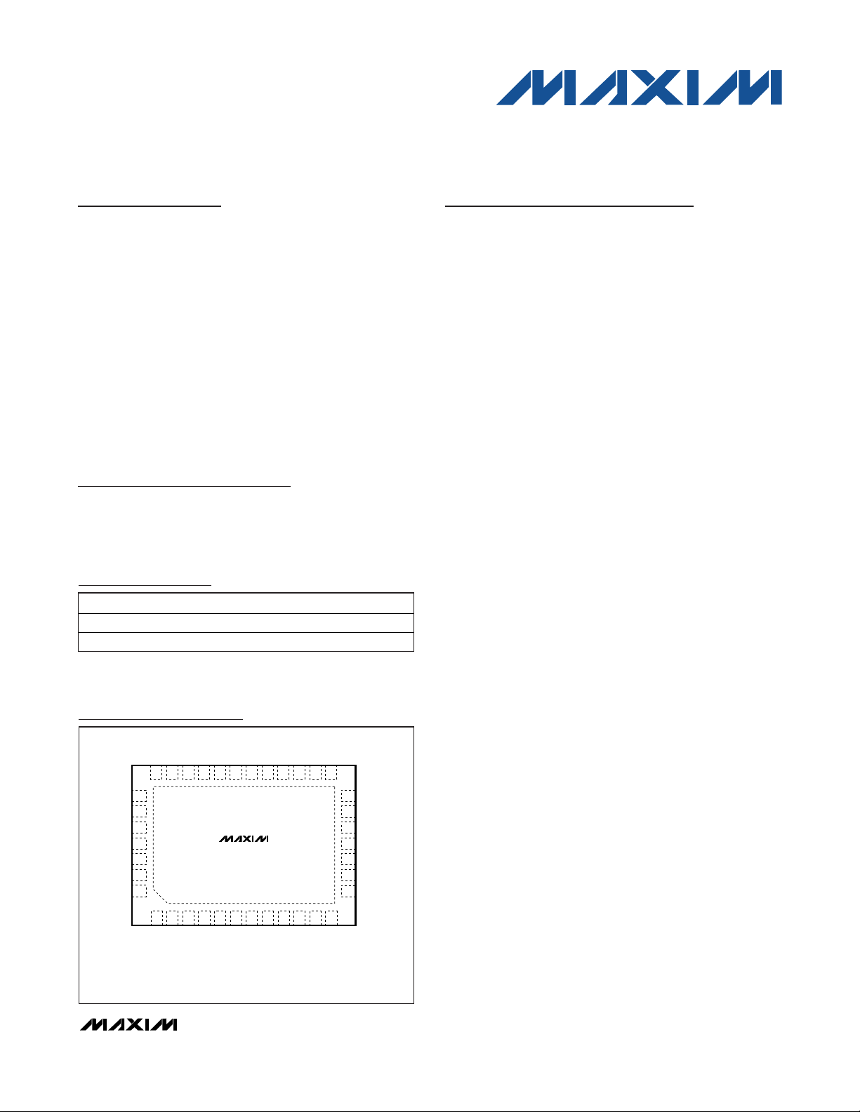
Pin Configuration
Ordering Information
Rev 1; 10/08
For pricing, delivery, and ordering information, please contact Maxim Direct at 1-888-629-4642,
or visit Maxim’s website at www.maxim-ic.com.
+
Denotes a lead-free/RoHS-compliant package.
T&R = Tape and reel.
*
EP = Exposed pad.
PON Triplexer and SFP Controller
PART TEMP RANGE PIN-PACKAGE
DS1875T+ -40°C to +95°C 38 TQFN-EP*
DS1875T+T&R -40°C to +95°C 38 TQFN-EP*
TOP VIEW
GND
GND
SW
V
N.C.
N.C.
N.C.
CC
V
31 30 29 28 27 26 25 24 23 22 21 20
32
33
34
35
CC
36
37
38
+
123456789101112
BEN
*EXPOSED PAD.
BMD
SDA
MOD
COMP
SCL
TX-F
(5mm
M4DAC
FB
BIAS
DS1875
N.C.
N.C.
FETG
TQFN
7mm × 0.8mm)
GND
TX-D
DAC1
CC
V
MON3P
GND
MON3N
*EP
N.C.
N.C.
LOSI
19
18
17
16
15
14
13
MON4
MON2
MON1
MON8/D3
MON7/D2
MON6/D1
MON5/D0
Page 2

DS1875
2 _______________________________________________________________________________________
Absolute Maximum Ratings . . . . . . . . . . . . . . . . . . . . . . . . . . . . . . . . . . . . . . . . . . . . . . . . . . . . . . . . . . . . . . . . . . . . . .5
Recommended Operating Conditions . . . . . . . . . . . . . . . . . . . . . . . . . . . . . . . . . . . . . . . . . . . . . . . . . . . . . . . . . . . . . .5
AC Electrical Characteristics . . . . . . . . . . . . . . . . . . . . . . . . . . . . . . . . . . . . . . . . . . . . . . . . . . . . . . . . . . . . . . . . . . . . .5
Electrical Characteristics (DAC1 and M4DAC) . . . . . . . . . . . . . . . . . . . . . . . . . . . . . . . . . . . . . . . . . . . . . . . . . . . . . . .6
Analog Input Characteristics (BMD, TXP HI, TXP LO, HBIAS) . . . . . . . . . . . . . . . . . . . . . . . . . . . . . . . . . . . . . . . . . . .6
Analog Output Characteristics . . . . . . . . . . . . . . . . . . . . . . . . . . . . . . . . . . . . . . . . . . . . . . . . . . . . . . . . . . . . . . . . . . . .6
PWM Characteristics . . . . . . . . . . . . . . . . . . . . . . . . . . . . . . . . . . . . . . . . . . . . . . . . . . . . . . . . . . . . . . . . . . . . . . . . . . .7
Timing Characteristics (Control Loop and Quick Trip) . . . . . . . . . . . . . . . . . . . . . . . . . . . . . . . . . . . . . . . . . . . . . . . . .7
Analog Voltage Monitoring . . . . . . . . . . . . . . . . . . . . . . . . . . . . . . . . . . . . . . . . . . . . . . . . . . . . . . . . . . . . . . . . . . . . . . .8
Digital Thermometer . . . . . . . . . . . . . . . . . . . . . . . . . . . . . . . . . . . . . . . . . . . . . . . . . . . . . . . . . . . . . . . . . . . . . . . . . . . .8
Nonvolatile Memory Characteristics . . . . . . . . . . . . . . . . . . . . . . . . . . . . . . . . . . . . . . . . . . . . . . . . . . . . . . . . . . . . . . .8
I
2
C Timing Specifications . . . . . . . . . . . . . . . . . . . . . . . . . . . . . . . . . . . . . . . . . . . . . . . . . . . . . . . . . . . . . . . . . . . . . . . .9
Typical Operating Characteristics . . . . . . . . . . . . . . . . . . . . . . . . . . . . . . . . . . . . . . . . . . . . . . . . . . . . . . . . . . . . . . . .10
Pin Description . . . . . . . . . . . . . . . . . . . . . . . . . . . . . . . . . . . . . . . . . . . . . . . . . . . . . . . . . . . . . . . . . . . . . . . . . . . . . . .13
Block Diagram . . . . . . . . . . . . . . . . . . . . . . . . . . . . . . . . . . . . . . . . . . . . . . . . . . . . . . . . . . . . . . . . . . . . . . . . . . . . . . .14
Typical Operating Circuit . . . . . . . . . . . . . . . . . . . . . . . . . . . . . . . . . . . . . . . . . . . . . . . . . . . . . . . . . . . . . . . . . . . . . . .15
Detailed Description . . . . . . . . . . . . . . . . . . . . . . . . . . . . . . . . . . . . . . . . . . . . . . . . . . . . . . . . . . . . . . . . . . . . . . . . . . .16
Bias Control . . . . . . . . . . . . . . . . . . . . . . . . . . . . . . . . . . . . . . . . . . . . . . . . . . . . . . . . . . . . . . . . . . . . . . . . . . . . . . .16
Autodetect Bias Control . . . . . . . . . . . . . . . . . . . . . . . . . . . . . . . . . . . . . . . . . . . . . . . . . . . . . . . . . . . . . . . . . .16
Open-Loop Bias Control . . . . . . . . . . . . . . . . . . . . . . . . . . . . . . . . . . . . . . . . . . . . . . . . . . . . . . . . . . . . . . . . . .16
Closed-Loop Bias Control . . . . . . . . . . . . . . . . . . . . . . . . . . . . . . . . . . . . . . . . . . . . . . . . . . . . . . . . . . . . . . . . .16
DC Operation . . . . . . . . . . . . . . . . . . . . . . . . . . . . . . . . . . . . . . . . . . . . . . . . . . . . . . . . . . . . . . . . . . . . . . . . . .17
Modulation Control . . . . . . . . . . . . . . . . . . . . . . . . . . . . . . . . . . . . . . . . . . . . . . . . . . . . . . . . . . . . . . . . . . . . . . . . .17
BIAS and MOD Output During Power-Up . . . . . . . . . . . . . . . . . . . . . . . . . . . . . . . . . . . . . . . . . . . . . . . . . . . . . . . .17
BIAS and MOD Output as a Function of Transmit Disable (TX-D) . . . . . . . . . . . . . . . . . . . . . . . . . . . . . . . . . . . . .18
APC and Quick-Trip Shared Comparator Timing . . . . . . . . . . . . . . . . . . . . . . . . . . . . . . . . . . . . . . . . . . . . . . . . . .18
Monitors and Fault Detection . . . . . . . . . . . . . . . . . . . . . . . . . . . . . . . . . . . . . . . . . . . . . . . . . . . . . . . . . . . . . . . . .19
Monitors . . . . . . . . . . . . . . . . . . . . . . . . . . . . . . . . . . . . . . . . . . . . . . . . . . . . . . . . . . . . . . . . . . . . . . . . . . . . . .19
Power-On Analog (POA) . . . . . . . . . . . . . . . . . . . . . . . . . . . . . . . . . . . . . . . . . . . . . . . . . . . . . . . . . . . . . . . . . .19
Quick-Trip Monitors and Alarms . . . . . . . . . . . . . . . . . . . . . . . . . . . . . . . . . . . . . . . . . . . . . . . . . . . . . . . . . . . .19
MON3 Quick Trip . . . . . . . . . . . . . . . . . . . . . . . . . . . . . . . . . . . . . . . . . . . . . . . . . . . . . . . . . . . . . . . . . . . . . . .19
ADC Monitors and Alarms . . . . . . . . . . . . . . . . . . . . . . . . . . . . . . . . . . . . . . . . . . . . . . . . . . . . . . . . . . . . . . . .19
ADC Timing . . . . . . . . . . . . . . . . . . . . . . . . . . . . . . . . . . . . . . . . . . . . . . . . . . . . . . . . . . . . . . . . . . . . . . . . . . . .20
Right-Shifting ADC Result . . . . . . . . . . . . . . . . . . . . . . . . . . . . . . . . . . . . . . . . . . . . . . . . . . . . . . . . . . . . . . . . .21
Transmit Fault (TX-F) Output . . . . . . . . . . . . . . . . . . . . . . . . . . . . . . . . . . . . . . . . . . . . . . . . . . . . . . . . . . . . . . . . . .21
Safety Shutdown (FETG) Output . . . . . . . . . . . . . . . . . . . . . . . . . . . . . . . . . . . . . . . . . . . . . . . . . . . . . . . . . . . . . . .22
Determining Alarm Causes Using the I
2
C Interface . . . . . . . . . . . . . . . . . . . . . . . . . . . . . . . . . . . . . . . . . . . . . . . .22
TABLE OF CONTENTS
PON Triplexer and SFP Controller
Page 3

DS1875
_______________________________________________________________________________________ 3
Die Identification . . . . . . . . . . . . . . . . . . . . . . . . . . . . . . . . . . . . . . . . . . . . . . . . . . . . . . . . . . . . . . . . . . . . . . . . . . .23
Low-Voltage Operation . . . . . . . . . . . . . . . . . . . . . . . . . . . . . . . . . . . . . . . . . . . . . . . . . . . . . . . . . . . . . . . . . . . . . .23
Enhanced RSSI Monitoring (Dual Range Functionality) . . . . . . . . . . . . . . . . . . . . . . . . . . . . . . . . . . . . . . . . . . . . .23
PWM Controller . . . . . . . . . . . . . . . . . . . . . . . . . . . . . . . . . . . . . . . . . . . . . . . . . . . . . . . . . . . . . . . . . . . . . . . . . . . .25
Inductor Selection . . . . . . . . . . . . . . . . . . . . . . . . . . . . . . . . . . . . . . . . . . . . . . . . . . . . . . . . . . . . . . . . . . . . . . .26
Stability and Compensation Component Selection . . . . . . . . . . . . . . . . . . . . . . . . . . . . . . . . . . . . . . . . . . . . .27
DAC1 Output . . . . . . . . . . . . . . . . . . . . . . . . . . . . . . . . . . . . . . . . . . . . . . . . . . . . . . . . . . . . . . . . . . . . . . . . . . . . . .27
M4DAC Output . . . . . . . . . . . . . . . . . . . . . . . . . . . . . . . . . . . . . . . . . . . . . . . . . . . . . . . . . . . . . . . . . . . . . . . . . . . .27
Digital I/O Pins . . . . . . . . . . . . . . . . . . . . . . . . . . . . . . . . . . . . . . . . . . . . . . . . . . . . . . . . . . . . . . . . . . . . . . . . . . . . .27
I
2
C Communication . . . . . . . . . . . . . . . . . . . . . . . . . . . . . . . . . . . . . . . . . . . . . . . . . . . . . . . . . . . . . . . . . . . . . . . . . . .29
I2C Definitions . . . . . . . . . . . . . . . . . . . . . . . . . . . . . . . . . . . . . . . . . . . . . . . . . . . . . . . . . . . . . . . . . . . . . . . . . . . . .29
I2C Protocol . . . . . . . . . . . . . . . . . . . . . . . . . . . . . . . . . . . . . . . . . . . . . . . . . . . . . . . . . . . . . . . . . . . . . . . . . . . . . . .30
Memory Map . . . . . . . . . . . . . . . . . . . . . . . . . . . . . . . . . . . . . . . . . . . . . . . . . . . . . . . . . . . . . . . . . . . . . . . . . . . . . . . .31
Memory Organization . . . . . . . . . . . . . . . . . . . . . . . . . . . . . . . . . . . . . . . . . . . . . . . . . . . . . . . . . . . . . . . . . . . . . . .31
Shadowed EEPROM . . . . . . . . . . . . . . . . . . . . . . . . . . . . . . . . . . . . . . . . . . . . . . . . . . . . . . . . . . . . . . . . . . . . . . . .32
Register Descriptions . . . . . . . . . . . . . . . . . . . . . . . . . . . . . . . . . . . . . . . . . . . . . . . . . . . . . . . . . . . . . . . . . . . . . . . . . .33
Lower Memory Register Map . . . . . . . . . . . . . . . . . . . . . . . . . . . . . . . . . . . . . . . . . . . . . . . . . . . . . . . . . . . . . . . . .33
Table 00h Register Map . . . . . . . . . . . . . . . . . . . . . . . . . . . . . . . . . . . . . . . . . . . . . . . . . . . . . . . . . . . . . . . . . . . . .34
Table 01h Register Map . . . . . . . . . . . . . . . . . . . . . . . . . . . . . . . . . . . . . . . . . . . . . . . . . . . . . . . . . . . . . . . . . . . . .35
Table 02h Register Map . . . . . . . . . . . . . . . . . . . . . . . . . . . . . . . . . . . . . . . . . . . . . . . . . . . . . . . . . . . . . . . . . . . . .36
Table 03h Register Map . . . . . . . . . . . . . . . . . . . . . . . . . . . . . . . . . . . . . . . . . . . . . . . . . . . . . . . . . . . . . . . . . . . . .37
Table 04h Register Map . . . . . . . . . . . . . . . . . . . . . . . . . . . . . . . . . . . . . . . . . . . . . . . . . . . . . . . . . . . . . . . . . . . . .38
Table 05h Register Map . . . . . . . . . . . . . . . . . . . . . . . . . . . . . . . . . . . . . . . . . . . . . . . . . . . . . . . . . . . . . . . . . . . . .38
Table 06h Register Map . . . . . . . . . . . . . . . . . . . . . . . . . . . . . . . . . . . . . . . . . . . . . . . . . . . . . . . . . . . . . . . . . . . . .39
Table 07h Register Map . . . . . . . . . . . . . . . . . . . . . . . . . . . . . . . . . . . . . . . . . . . . . . . . . . . . . . . . . . . . . . . . . . . . .39
Table 08h Register Map . . . . . . . . . . . . . . . . . . . . . . . . . . . . . . . . . . . . . . . . . . . . . . . . . . . . . . . . . . . . . . . . . . . . .40
Auxiliary A0h Memory Register Map . . . . . . . . . . . . . . . . . . . . . . . . . . . . . . . . . . . . . . . . . . . . . . . . . . . . . . . . . . . .41
Lower Memory Register Descriptions . . . . . . . . . . . . . . . . . . . . . . . . . . . . . . . . . . . . . . . . . . . . . . . . . . . . . . . . . . .42
Table 00h Register Descriptions . . . . . . . . . . . . . . . . . . . . . . . . . . . . . . . . . . . . . . . . . . . . . . . . . . . . . . . . . . . . . . .57
Table 01h Register Descriptions . . . . . . . . . . . . . . . . . . . . . . . . . . . . . . . . . . . . . . . . . . . . . . . . . . . . . . . . . . . . . . .57
Table 02h Register Descriptions . . . . . . . . . . . . . . . . . . . . . . . . . . . . . . . . . . . . . . . . . . . . . . . . . . . . . . . . . . . . . . .61
Table 03h Register Descriptions . . . . . . . . . . . . . . . . . . . . . . . . . . . . . . . . . . . . . . . . . . . . . . . . . . . . . . . . . . . . . . .87
Table 04h Register Descriptions . . . . . . . . . . . . . . . . . . . . . . . . . . . . . . . . . . . . . . . . . . . . . . . . . . . . . . . . . . . . . . .87
Table 05h Register Descriptions . . . . . . . . . . . . . . . . . . . . . . . . . . . . . . . . . . . . . . . . . . . . . . . . . . . . . . . . . . . . . . .88
Table 06h Register Descriptions . . . . . . . . . . . . . . . . . . . . . . . . . . . . . . . . . . . . . . . . . . . . . . . . . . . . . . . . . . . . . . .89
Table 07h Register Descriptions . . . . . . . . . . . . . . . . . . . . . . . . . . . . . . . . . . . . . . . . . . . . . . . . . . . . . . . . . . . . . . .90
Table 08h Register Descriptions . . . . . . . . . . . . . . . . . . . . . . . . . . . . . . . . . . . . . . . . . . . . . . . . . . . . . . . . . . . . . . .91
TABLE OF CONTENTS (continued)
PON Triplexer and SFP Controller
Page 4

DS1875
PON Triplexer and SFP Controller
4 _______________________________________________________________________________________
Auxiliary Memory A0h Register Descriptions . . . . . . . . . . . . . . . . . . . . . . . . . . . . . . . . . . . . . . . . . . . . . . . . . . . . .91
Package Information . . . . . . . . . . . . . . . . . . . . . . . . . . . . . . . . . . . . . . . . . . . . . . . . . . . . . . . . . . . . . . . . . . . . . . . . . .91
TABLE OF CONTENTS (continued)
Figure 1. Power-Up Timing (BEN is a Long Burst) . . . . . . . . . . . . . . . . . . . . . . . . . . . . . . . . . . . . . . . . . . . . . . . . . . . .17
Figure 2. TX-D Timing . . . . . . . . . . . . . . . . . . . . . . . . . . . . . . . . . . . . . . . . . . . . . . . . . . . . . . . . . . . . . . . . . . . . . . . . .18
Figure 3. APC Loop and Quick-Trip Sample Timing . . . . . . . . . . . . . . . . . . . . . . . . . . . . . . . . . . . . . . . . . . . . . . . . . .18
Figure 4. M3QT Timing . . . . . . . . . . . . . . . . . . . . . . . . . . . . . . . . . . . . . . . . . . . . . . . . . . . . . . . . . . . . . . . . . . . . . . . . .20
Figure 5. ADC Timing with EN5TO8B = 0 . . . . . . . . . . . . . . . . . . . . . . . . . . . . . . . . . . . . . . . . . . . . . . . . . . . . . . . . . .20
Figure 6. ADC Timing with EN5TO8B = 1 . . . . . . . . . . . . . . . . . . . . . . . . . . . . . . . . . . . . . . . . . . . . . . . . . . . . . . . . . .20
Figure 7. TX-F Timing . . . . . . . . . . . . . . . . . . . . . . . . . . . . . . . . . . . . . . . . . . . . . . . . . . . . . . . . . . . . . . . . . . . . . . . . . .21
Figure 8. FETG/Output Disable Timing (Fault Condition Detected) . . . . . . . . . . . . . . . . . . . . . . . . . . . . . . . . . . . . . . .22
Figure 9. SEE Timing . . . . . . . . . . . . . . . . . . . . . . . . . . . . . . . . . . . . . . . . . . . . . . . . . . . . . . . . . . . . . . . . . . . . . . . . . .23
Figure 10. RSSI Flowchart . . . . . . . . . . . . . . . . . . . . . . . . . . . . . . . . . . . . . . . . . . . . . . . . . . . . . . . . . . . . . . . . . . . . . .24
Figure 11. PWM Controller Diagram . . . . . . . . . . . . . . . . . . . . . . . . . . . . . . . . . . . . . . . . . . . . . . . . . . . . . . . . . . . . . .25
Figure 12. PWM Controller Typical APD Bias Circuit . . . . . . . . . . . . . . . . . . . . . . . . . . . . . . . . . . . . . . . . . . . . . . . . . .28
Figure 13. PWM Controller Voltage Output Configuration . . . . . . . . . . . . . . . . . . . . . . . . . . . . . . . . . . . . . . . . . . . . . .28
Figure 14. PWM Controller Current-Sink Output Configuration . . . . . . . . . . . . . . . . . . . . . . . . . . . . . . . . . . . . . . . . . .28
Figure 15. I
2
C Timing Diagram . . . . . . . . . . . . . . . . . . . . . . . . . . . . . . . . . . . . . . . . . . . . . . . . . . . . . . . . . . . . . . . . . .29
Figure 16. Memory Map . . . . . . . . . . . . . . . . . . . . . . . . . . . . . . . . . . . . . . . . . . . . . . . . . . . . . . . . . . . . . . . . . . . . . . . .32
Table 1. DS1875 Acronyms . . . . . . . . . . . . . . . . . . . . . . . . . . . . . . . . . . . . . . . . . . . . . . . . . . . . . . . . . . . . . . . . . . . . .16
Table 2. Update Rate Timing . . . . . . . . . . . . . . . . . . . . . . . . . . . . . . . . . . . . . . . . . . . . . . . . . . . . . . . . . . . . . . . . . . . .18
Table 3. ADC Default Monitor Ranges . . . . . . . . . . . . . . . . . . . . . . . . . . . . . . . . . . . . . . . . . . . . . . . . . . . . . . . . . . . . .20
Table 4. TX-F as a Function of TX-D and Alarm Sources . . . . . . . . . . . . . . . . . . . . . . . . . . . . . . . . . . . . . . . . . . . . . . .21
Table 5. FETG, MOD, and BIAS Outputs as a Function of TX-D and Alarm Sources . . . . . . . . . . . . . . . . . . . . . . . . .22
Table 6. MON3 Configuration Registers . . . . . . . . . . . . . . . . . . . . . . . . . . . . . . . . . . . . . . . . . . . . . . . . . . . . . . . . . . .24
Table 7. MON3 Hysteresis Threshold Values . . . . . . . . . . . . . . . . . . . . . . . . . . . . . . . . . . . . . . . . . . . . . . . . . . . . . . .25
LIST OF FIGURES
LIST OF TABLES
Page 5
DS1875
Stresses beyond those listed under “Absolute Maximum Ratings” may cause permanent damage to the device. These are stress ratings only, and functional
operation of the device at these or any other conditions beyond those indicated in the operational sections of the specifications is not implied. Exposure to
absolute maximum rating conditions for extended periods may affect device reliability.
Voltage Range on MON1–MON8,
BEN, BMD, and TX-D Pins
Relative to Ground .................................-0.5V to (V
CC
+ 0.5V)*
Voltage Range on V
CC
, SDA, SCL,
D0–D3, and TX-F Pins Relative to Ground...............-0.5V to 6V
Operating Temperature Range ...........................-40°C to +95°C
Programming Temperature Range .........................0°C to +85°C
Storage Temperature Range .............................-55°C to +125°C
Soldering Temperature...........................Refer to the IPC/JEDEC
J-STD-020 Specification.
AC ELECTRICAL CHARACTERISTICS
(VCC= +2.85V to +3.9V, TA= -40°C to +95°C, unless otherwise noted.)
*
Subject to not exceeding +6V.
RECOMMENDED OPERATING CONDITIONS
(TA= -40°C to +95°C, unless otherwise noted.)
ABSOLUTE MAXIMUM RATINGS
PON Triplexer and SFP Controller
_______________________________________________________________________________________ 5
Main Supply Voltage VCC (Note 1) +2.85 +3.9 V
High-Level Input Voltage
(SDA, SCL, BEN)
Low-Leve l Input Voltage
(SDA, SCL, BEN)
High-Level Input Voltage
(TX-D, LOSI, D0, D1, D2, D3)
Low-Leve l Input Voltage
(TX-D, LOSI, D0, D1, D2, D3)
PARAMETER SYMBOL CONDITIONS MIN TYP MAX UNITS
V
IH:1
V
-0.3
IL:1
V
2.0
IH:2
V
-0.3 +0.8 V
IL:2
0.7 x
V
CC
V
CC
0.3
0.3 x
V
CC
V
CC
0.3
+
V
V
+
V
PARAMETER SYMBOL CONDITIONS MIN TYP MAX UNITS
Supply Current ICC (Notes 1, 2) 5.5 10 mA
Output Leakage
(SDA, TX-F, D0, D1, D2, D3)
Low-Leve l Output Voltage
(SDA, TX-F, FETG, D0, D1, D2, D3)
High-Level Output Voltage
(FETG)
FETG Before Recall (Note 3) 10 100 nA
Input Leakage Current
(SCL, BEN, TX-D, LOSI)
Digital Power-On Reset POD 1.0 2.2 V
Analog Power-On Reset POA 2.1 2.75 V
I
(Note 2) 1 μA
LO
V
V
I
OH
LI:1
IOL = 4mA 0.4
OL
IOL = 6mA 0.6
V
-
IOH = 4mA
1 μA
CC
0.4
V
V
Page 6
DS1875
PON Triplexer and SFP Controller
6 _______________________________________________________________________________________
ANALOG OUTPUT CHARACTERISTICS
(VCC= +2.85V to +3.9V, TA= -40°C to +95°C, unless otherwise noted.)
ANALOG INPUT CHARACTERISTICS (BMD, TXP HI, TXP LO, HBIAS)
(VCC= +2.85V to +3.9V, TA= -40°C to +95°C, unless otherwise noted.)
ELECTRICAL CHARACTERISTICS (DAC1 AND M4DAC)
(VCC= +2.85V to +3.9V, TA= -40°C to +95°C, unless otherwise noted.)
DAC Output Range 2.5 V
DAC Output Resolution 8 Bits
DAC Output Integral Nonlinearity -1 +1 LSB
DAC Output Differential
Nonlinearity
DAC Error TA = +25°C -1.25 +1.25 %FS
DAC Temperature Drift -2 +2 %FS
DAC Offset -12 +12 mV
Max imum Load -500 +500 μA
Maximum Load Capacitance 250 pF
BMD, TXP HI, TXP LO Full-Scale
Voltage
HBIAS Full-Scale Voltage (Note 5) 1.25 V
BMD Input Resistance 35 50 65 k
Resolution 8 Bits
Error TA = +25°C (Note 6) ±2 %FS
Integral Nonlinearity -1 +1 LSB
Differentia l Nonl inearit y -1 +1 LSB
Temperature Drift -2.5 +2.5 %FS
PARAMETER SYMBOL CONDITIONS MIN TYP MAX UNITS
-1 +1 LSB
PARAMETER SYMBOL CONDITIONS MIN TYP MAX UNITS
(Note 4) 2.5 V
V
APC
PARAMETER SYMBOL CONDITIONS MIN TYP MAX UNITS
BIAS Current I
I
Shutdown Current I
BIAS
Voltage at I
MOD Full-Scale Voltage V
MOD Output Impedance (Note 7) 3 k
V
Error TA = +25°C (Note 8) -1.25 +1.25 %FS
MOD
V
Integral Nonlinearity -1 +1 LSB
MOD
V
Differentia l Nonl inearit y -1 +1 LSB
MOD
V
Temperature Drift -2 +2 %FS
MOD
0.7 1.2 1.4 V
BIAS
(Note 1) 1.2 mA
BIAS
BIAS:OFF
10 100 nA
(Note 5) 1.25 V
MOD
Page 7
DS1875
TIMING CHARACTERISTICS (CONTROL LOOP AND QUICK TRIP)
(VCC= +2.85V to +3.9V, TA= -40°C to +95°C, unless otherwise noted.)
PWM CHARACTERISTICS
(VCC= +2.85V to +3.9V, TA= -40°C to +95°C, unless otherwise noted.)
PON Triplexer and SFP Controller
_______________________________________________________________________________________ 7
PWM-DAC Full-Scale Voltage V
PWM-DAC Resolution 8 Bit s
V
PWM-DAC
Error
V
PWM-DAC
V
PWM-DAC
Nonlinearity
V
PWM-DAC
SW Output Impedance 20
SW Frequency Error f
SW Dut y C ycle D
Error-Amplifier Source Current -10 μA
Error-Amplifier Sink Current +10 μA
COMP High-Voltage Clamp 2.1 V
COMP Low-Voltage Clamp 0.8 V
Error-Amplifier
Transconductance
Error-Amplifier Output
Impedance
FB Pin Capacitance 5 pF
PARAMETER SYMBOL CONDITIONS MIN TYP MAX UNITS
PWM-DAC
Full-Scale Voltage
Integral Nonlinearity -1 1 LSB
Differential
Temperature Drift -2 +2 %FS
1.25 V
T
-1 1 LSB
SWER
MAX
G
M
260 M
R
EA
= +25°C 1.25 %
A
(Note 9) -5 +7 %
89 90 91 %
425 μS
First BMD Sample Following BEN t
Remaining Updates During BEN t
BEN High Time t
BEN Low Time t
Output-Enable Time Following POA t
BIAS and MOD Turn-Off Delay t
BIAS and MOD Turn-On Delay tON 5 μs
FETG Turn-On Delay t
FETG Turn-Off Delay t
PARAMETER SYMBOL CONDITIONS MIN TYP MAX UNITS
(Note 10)
FIRST
(Note 10)
UPDATE
BEN:HIGH
BEN:LOW
FETG:ON
FETG:OFF
400 ns
96 ns
10 ms
INIT
5 μs
OFF
5 μs
5 μs
Page 8
DS1875
PON Triplexer and SFP Controller
8 _______________________________________________________________________________________
NONVOLATILE MEMORY CHARACTERISTICS
(VCC= +2.85V to +3.9V, TA= -40°C to +95°C, unless otherwise noted.)
DIGITAL THERMOMETER
(VCC= +2.85V to +3.9V, TA= -40°C to +95°C, unless otherwise noted.)
ANALOG VOLTAGE MONITORING
(VCC= +2.85V to +3.9V, TA= -40°C to +95°C, unless otherwise noted.)
PARAMETER SYMBOL CONDITIONS MIN TYP MAX UNITS
ADC Re solution 13 Bits
Input/Supply Accuracy
(MON1–MON8, V
Update Rate for Temp,
MON1–MON4, and V
Update Rate for MON5–MON8 t
Input/Supply Offset
(MON1–MON8, V
Factor y Setting
)
CC
CC
)
CC
MON1–MON8 2.5
V
CC
MON3 Fine
Thermometer Error T
PARAMETER SYMBOL CONDITIONS MIN TYP MAX UNITS
ACC At factory sett ing 0.25 0.50 %FS
t
FRAME:1
FRAME:2
78 95 ms
Bit EN5TO8B is enabled in Table 02h,
Regi ster 89h
V
(Note 11) 0 5 LSB
OS
Ful l sca le s are user programmable
-40°C to +95°C ±3.0 °C
ERR
156 190 ms
6.5536
312.5 μV
V
EEPROM Write Cycles
PARAMETER SYMBOL CONDITIONS MIN TYP MAX UNITS
At +85°C (Note 11) 50,000
At +25°C (Note 11) 200,000
Page 9

DS1875
Note 1: All voltages are referenced to ground. Current into IC is positive, and current out of the IC is negative.
Note 2: Digital inputs are at rail. FETG is disconnected. SDA = SCL = V
CC
. SW, DAC1, and M4DAC are not loaded.
Note 3: See the
Safety Shutdown (FETG) Output
section for details.
Note 4: Eight ranges allow the full scale to change from 625mV to 2.5V.
Note 5: Eight ranges allow the full scale to change from 312.5mV to 1.25V.
Note 6: This specification applies to the expected full-scale value for the selected range. See the COMP RANGING register
description for available full-scale ranges.
Note 7: The output impedance of the DS1875 is proportional to its scale setting. For instance, if using the 1/2 scale, the output
impedance would be approximately 1.56kΩ.
Note 8: This specification applies to the expected full-scale value for the selected range. See the MOD RANGING register
description for available full-scale ranges.
Note 9: The switching frequency is selectable between four values: 131.25kHz, 262.5kHz, 525kHz, and 1050kHz.
Note 10: See the
APC and Quick-Trip Shared Comparator Timing
section for details.
Note 11: Guaranteed by design.
Note 12: I
2
C interface timing shown is for fast-mode (400kHz) operation. This device is also backward compatible with I2C stan-
dard mode.
Note 13: C
B
—Total capacitance of one bus line in pF.
Note 14: EEPROM write begins after a STOP condition occurs.
I2C TIMING SPECIFICATIONS
(VCC= +2.85V to +3.9V, TA= -40°C to +95°C, timing referenced to V
IL(MAX)
and V
IH(MIN)
.) (See Figure 15.)
PON Triplexer and SFP Controller
_______________________________________________________________________________________ 9
SCL Clock Frequency f
Cloc k Pulse-Width Low t
Cloc k Pulse-Width High t
Bus-Free Time Between STOP
and START Condition
START Hold Time t
START Setup Time t
Data in Hold Time t
Data in Setup Time t
Capacitive Load for Each Bus Line CB 400 pF
Rise Time of Both SDA and SCL
Signals
Fal l Time of Both SDA and SCL
Signals
STOP Setup Time t
EEPROM Write Time tW (Note 14) 20 ms
PARAMETER SYMBOL CONDITIONS MIN TYP MAX UNITS
(Note 12) 0 400 kH z
SCL
1.3 μs
LOW
0.6 μs
HIGH
t
1.3 μs
BUF
0.6 μs
HD: STA
0.6 μs
SU:STA
0 0.9 μs
HD:DAT
100 ns
SU:DAT
t
(Note 13)
R
t
(Note 13)
F
0.6 μs
SU:STO
20 +
0.1C
20 +
0.1C
300 ns
B
300 ns
B
Page 10
DS1875
PON Triplexer and SFP Controller
10 ______________________________________________________________________________________
Typical Operating Characteristics
(VCC= +2.85V to +3.9V, TA= +25°C, unless otherwise noted.)
9.0
SDA = SCL = V
8.5
8.0
7.5
7.0
6.5
6.0
SUPPLY CURRENT (mA)
5.5
5.0
4.5
2.85
SUPPLY CURRENT vs. TEMPERATURE
V
CC
SW = 525kHz
SW = 262.5kHz
-40
(mA)
CC
I
8.8
8.6
8.4
8.2
8.0
7.8
7.6
7.4
SUPPLY CURRENT
vs. SUPPLY VOLTAGE
CC
+95°C
+25°C
-40°C
VCC (V)
= 5V, NO BIAS CURRENT
SW = 1050kHz
SW = 131.25kHz
TEMPERATURE (°C)
SUPPLY CURRENT
vs. TEMPERATURE
9.0
SDA = SCL = V
DS1875 toc01
3.853.35
8.5
8.0
7.5
7.0
6.5
6.0
SUPPLY CURRENT (mA)
5.5
5.0
4.5
-40
CC
VCC = 3.9V
VCC = 2.85V
TEMPERATURE (°C)
DS1875 toc02
806020 400-20
DAC1 AND M4DAC DNL
1.0
DS1875 toc04
806040200-20
0.8
0.6
0.4
0.2
0
-0.2
-0.4
DAC1 AND M4DAC DNL (LSB)
-0.6
-0.8
-1.0
0
DAC1 AND M4DAC POSITION (DEC)
DS1875 toc05
25020015010050
SUPPLY CURRENT vs. TEMPERATURE
V
= 3.3V, NO BIAS CURRENT
CC
SW = 1050kHz
SW = 525kHz
SW = 262.5kHz
SW = 131.25kHz
-40
TEMPERATURE (°C)
(mA)
CC
I
7.4
7.3
7.2
7.1
7.0
6.9
6.8
6.7
6.6
6.5
6.4
DAC1 AND M4DAC INL
1.0
0.8
0.6
0.4
0.2
0
-0.2
-0.4
DAC1 AND M4DAC INL (LSB)
-0.6
-0.8
-1.0
0
DAC1 AND M4DAC POSITION (DEC)
DS1875 toc03
806020 400-20
DS1875 toc06
25020015010050
DAC1 AND M4DAC OFFSET vs. V
0.05
TA = -40°C TO +95°C
0.04
LOAD = -0.5mA TO +0.5mA
0.03
0.02
0.01
0
-0.01
-0.02
DAC1 AND M4DAC OFFSET (mV)
-0.03
-0.04
-0.05
2.85
VCC (V)
DAC1 AND M4DAC OFFSET VARIATION
CC
3.853.653.453.253.05
0.0010
0.0008
DS1875 toc07
0.0006
0.0004
0.0002
0
-0.0002
-0.0004
DAC1 AND M4DAC OFFSET (mV)
-0.0006
-0.0008
-0.0010
-0.5 0.5
vs. LOAD CURRENT
VCC = 2.85V
VCC = 3.6V
VCC = 3.9V
LOAD CURRENT (mA)
1.259
DS1875 toc08
1.257
1.255
1.253
1.251
1.249
DAC1 AND M4DAC OUTPUT (V)
1.247
0.30.1-0.1-0.3
1.245
DAC1 AND M4DAC OUTPUT
vs. LOAD CURRENT
OUTPUT WITHOUT OFFSET
VCC = 2.85V
VCC = 3.9V
-0.5 0.5
LOAD CURRENT (mA)
DS1875 toc09
0.30.1-0.3 -0.1
Page 11
DS1875
Typical Operating Characteristics (continued)
(VCC= +2.85V to +3.9V, TA= +25°C, unless otherwise noted.)
CALCULATED AND DESIRED % CHANGE
IN V
MOD
vs. MOD RANGING
DS1875 toc10
MOD RANGING VALUE (DEC)
CHANGE IN V
MOD
(%)
007006004 005002 003001
10
20
30
40
50
60
70
80
90
100
0
000
CALCULATED
VALUE
DESIRED
VALUE
DESIRED AND CALCULATED CHANGE
IN V
BMD
vs. COMP RANGING
DS1875 toc11
COMP RANGING (DEC)
CHANGE IN V
BMD
(%)
111110100 101010 011001
10
20
30
40
50
60
70
80
90
100
0
000
CALCULATED
VALUE
DESIRED
VALUE
MON1 TO MON8 INL
DS1875 toc12
MON1 TO MON8 INPUT VOLTAGE (V)
MON1 TO MON8 INL (LSB)
2.01.51.00.5
-0.8
-0.6
-0.4
-0.2
0
0.2
0.4
0.6
0.8
1.0
-1.0
0 2.5
USING FACTORY-PROGRAMMED
FULL-SCALE VALUE OF 2.5V
MON1 TO MON8 DNL
DS1875 toc13
MON1 TO MON8 INPUT VOLTAGE (V)
MON1 TO MON8 DNL (LSB)
2.01.51.00.5
-0.8
-0.6
-0.4
-0.2
0
0.2
0.4
0.6
0.8
1.0
-1.0
0 2.5
USING FACTORY-PROGRAMMED
FULL-SCALE VALUE OF 2.5V
V
BMD
INL vs. APC INDEX
DS1875 toc14
APC INDEX (DEC)
V
BMD
INL (LSB)
25020015010050
-0.8
-0.6
-0.4
-0.2
0
0.2
0.4
0.6
0.8
1.0
-1.0
0
V
MOD
INL vs. MOD INDEX
DS1875 toc15
MOD INDEX (DEC)
V
MOD
INL (LSB)
25020015010050
-0.8
-0.6
-0.4
-0.2
0
0.2
0.4
0.6
0.8
1.0
-1.0
0
FB VOLTAGE vs. TEMPERATURE
PWM DAC = FFh
DS1875 toc16
TEMPERATURE (°C)
V
OUT
(V)
806040200-20
1.245
1.250
1.255
1.260
1.240
-40
V
OUT
vs. V
CC
VIN = 3.3V
DS1875 toc17
VCC (V)
V
OUT
(V)
3.853.35
75.2
75.4
75.6
75.8
76.0
76.2
76.4
76.6
76.8
77.0
75.0
2.85
DUTY-CYCLE LIMIT vs. TEMPERATURE
DS1875 toc18
TEMPERATURE (°C)
V
OUT
(V)
8060-20 0 20 40
89.25
89.50
89.75
90.00
90.25
90.50
90.75
91.00
89.00
-40
SW FREQUENCY
525kHz
262.5kHz
131.25kHZ
1050kHz
PON Triplexer and SFP Controller
______________________________________________________________________________________
11
Page 12
DS1875
PON Triplexer and SFP Controller
12 ______________________________________________________________________________________
μ
Typical Operating Characteristics (continued)
(VCC= +2.85V to +3.9V, TA= +25°C, unless otherwise noted.)
1.00
0.75
0.50
0.25
0
DAC DNL (LSB)
-0.25
-0.50
-0.75
-1.00
0 256
PWM DAC DNL
DAC SETTING (DEC)
1.00
0.75
0.50
0.25
0
DAC INL (LSB)
-0.25
-0.50
-0.75
-1.00
0 256
PWM DAC CHANGING FROM 00h TO 80h
20V/div
0V
200mV/div
0V
200mV/div
0V
R
COMP
V
FB
COMP
22419232 64 96 128 160
M3QT DAC INL
DAC SETTING (dec)
= 24.3kΩ, C
OUT
DUTY CYCLE
DS1875 toc19
5ms/div
1.00
PWM DAC INL
0.75
0.50
0.25
0
DAC INL (LSB)
-0.25
-0.50
-0.75
-1.00
0 256
DAC SETTING (DEC)
DS1875 toc22
22419232 64 96 128 160
= 220nF
COMP
DS1875 toc24
10%/div
0%
1V/div
10mA/div
0mA
5V/div
50V/div
100mA/div
0mA
100mV/div
1.00
0.75
DS1875 toc20
0.50
0.25
0
DAC DNL (LSB)
-0.25
-0.50
-0.75
-1.00
22419232 64 96 128 160
0 256
DAC SETTING (DEC)
SW CURRENT INTO BSS123 FET
M3QT DAC DNL
FREQUENCY = 1050kHz 50% DUTY CYCLE
SW
0V
SW
CURRENT
100ns/div
DS1875 toc23
SWITCHING WAVEFORMS
V
0V
0V
0V
= 3.3V, V
IN
V
OUT
RIPPLE (AC-COUPLED)
OUT
C2 = 0.1
INDUCTOR
VOLTAGE
INDUCTOR
CURRENT
~ 90V, I
2μs/div
OUT
F
~ 1.25mA,
DS1875 toc25
SW
DS1875 toc21
22419232 64 96 128 160
Page 13

DS1875
PON Triplexer and SFP Controller
______________________________________________________________________________________ 13
Pin Description
PIN NAME FUNCTION
1 BEN Burst-Enable Input. Triggers the samp les for the APC and quick-trip monitors.
2 SDA I2C Serial-Data Input/Output
3 SCL I2C Serial-Clock Input
4 TX-F Transm it-Fault Output
5, 7, 11, 20,
36, 37, 38
6 FETG
8 TX-D Transmit-Disable Input. Disables analog outputs.
9, 31, 35 VCC Power-Supply Input (2.85V to 3.9V)
10, 24, 32, 33 GND Ground Connection
12 LOSI
13 MON5/D0
14, 15, 16
17, 18, 19
21, 22
23 DAC1 8-Bit DAC Output. Driven either by I2C interface or temperature-indexed LUT.
25 M4DAC
26 FB
27 BIAS Bias-Current Output. This 13-bit current output generates the bias current reference for the MAX3643.
28 MOD
29 COMP Compensation for Error Amplifier in PWM Controller
30 BMD Back Mon itor Diode Input (Feedback Voltage, Transmit Power Mon itor)
34 SW
— EP Exposed Pad
N.C. No Connection
FET Gate Output. Signals an external n-channel or p-channel MOSFET to enable/disable the
laser’s current.
Loss-of-Signal Input. Open-collector buffer for external loss-of-signal input. This input is
accessible in the statu s regi ster through the I
External Monitor Input 5 or Digita l I/O 0. This signal i s the open-collector output driver for IN. It
can also be control led by the MUX0 and OUT0 bit s. The voltage level of this pin can be read at
IN0. In analog input mode, the voltage at this pin is digitized by the internal 13-bit analog-todigital converter and can be read through the I
assigned to interrupt the processor based on the ADC result.
External Monitor Inputs 6, 7, and 8 or Digital I/O 1, 2, and 3. In digital mode, these open-collector
MON6/D1,
MON7/D2,
MON8/D3
MON1,
MON2,
MON4
MON3N,
MON3P
outputs are controlled by the OUTx bits, and their voltage level s can be read at the INx bits. In
analog input mode, the voltages at these pins are digitized by the internal 13-bit analog-to-digital
converter and can be read through the I
to interrupt the processor based on the ADC result. D2 i s configurable a s a quick-trip output for
MON3.
External Monitor Input 1, 2, and 4. The voltage at these pins is digitized by the internal 13-bit
analog-to-digital converter and can be read through the I
can be ass igned to interrupt the processor based on the ADC result.
External Monitor Input 3. This is a differentia l input that is digitized by the internal 13-bit ADC
and can be read through the I
the processor based on the ADC result. When used as a s ingle-ended input, connect MON3N to
ground.
8-Bit DAC Output for Generating Analog Voltage. Can be controlled by a LUT indexed by the
voltage applied to MON4.
Converter Feedback. Input to error amplifier. The other input to the error amplifier is an 8-bit DAC.
The DAC can be driven by a temperature-indexed LUT. The output of the error amplifier is the
input of the comparator used to create the PWM signal.
Modulation Output Voltage. This 8-bit vo ltage output has eight full-scale ranges from 1.25V to
0.3125V. This pin is connected to the MAX3643’s VMSET input to control the modulation current.
PWM Output. This is typically the switching node of a PWM converter. In conjunction with FB, a
boost converter, buck converter, or analog 8-bit output can be created.
2
C interface.
2
C interface. Alarm and warning values can be
2
C interface. Alarm and warning values can be assigned
2
C interface. Alarm and warning values
2
C interface. Alarm and warning values can be assigned to interrupt
Page 14
DS1875
PON Triplexer and SFP Controller
14 ______________________________________________________________________________________
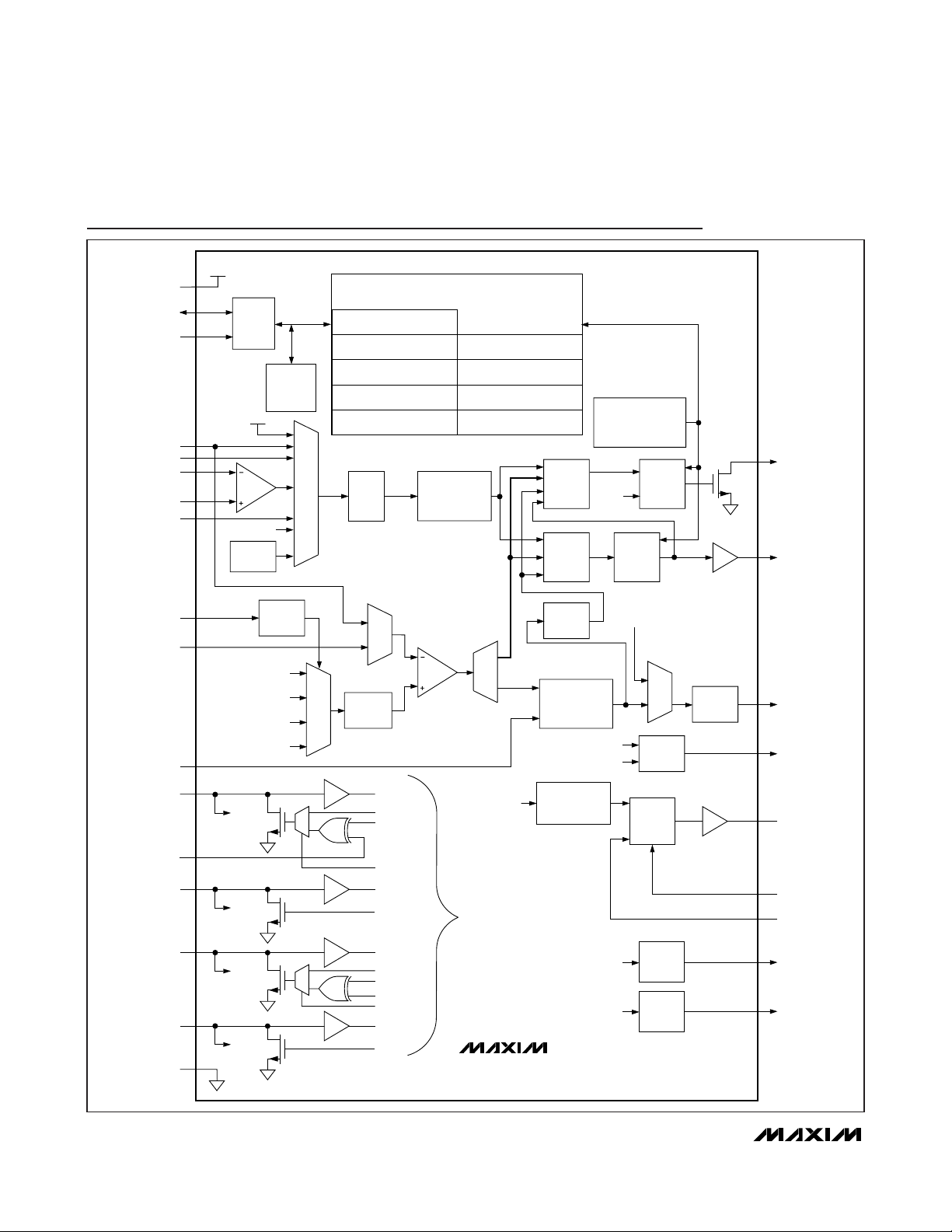
Block Diagram
V
CC
SDA
SCL
MON1
MON2
MON3N
MON3P
MON4
BEN
BMD
TX-D
MON5/D0
V
CC
2
C
I
INTERFACE
256 BYTES AT
V
CC
MON[5:8]
TEMP
SENSOR
SAMPLE
CONTROL
HBIAS
QUICK-TRIP LIMIT
HTXP
QUICK-TRIP LIMIT
LTXP
QUICK-TRIP LIMIT
APC SET POINT FROM
TRACKING-ERROR TABLE
MON5
EEPROM
A0h SLAVE
ADDRESS
DS1865 MEMORY ORGANIZATION
ADDITIONAL MONITORS
USER MEMORY, ALARM TRAP
CONFIGURATION AND CALIBRATION
13-BIT
ANALOG MUX
DAC WITH
MUX
SCALING
TTL
0
1
TTL
TABLE 00h (EEPROM)
TABLE 01h (EEPROM)
TABLE 02h (EEPROM)
TABLE 03h (EEPROM)
USER MEMORY
TABLE 04h (EEPROM)
MODULATION LUT
ADC
MUX
8-BIT
LOS STATUS/
D0 IN
D0 OUT
INV0
MAIN MEMORY
EEPROM/SRAM
ALARM/WARNING COMPARISONS
DIGITAL LIMIT
COMPARATOR FOR
ADC RESULTS
LUT CAN BE INDEXED BY
ADC CONFIGURATION/RESULTS
SYSTEM STATUS BITS
TABLE 05h (EEPROM)
ADC TE LUT
TABLE 06h (EEPROM)
M4DAC LUT
TABLE 07h (EEPROM)
PWM LUT
TABLE 08h (EEPROM)
BIAS OL LUT
INTERRUPT
INTERRUPT
BIAS MAX
QUICK TRIP
MUX
TABLE 07h
PWM VOLTAGE
TEMP SENSOR
MASK
MASK
DIGITAL
APC
INTEGRATOR
8-BIT
PWM-DAC
SRAM RESET
LATCH
ENABLE
TX-D INPUT
MOD LUT
POWER-ON ANALOG
> V
V
CC
POA
NONMASKABLE
INTERRUPT
INTERRUPT
LATCH
INTERRUPT
LATCH
TABLE 08h
BIAS OL LUT
TEMP INDEXED
MUX
8-BIT
DAC WITH
SCALING
PWM
13-BIT
DAC
TX-F
FETG
BIAS
MOD
SW
LOSI
MON6/D1
MON7/D2
MON8/D3
GND
MON6
MON7
MON8
TTL
TTL
0
1
TTL
TTL
MUX0
D1 IN
D1 OUT
D2 IN
D2 OUT
INV M3QT
M3QT
MUX2
D3 IN
D3 OUT
I2C CONTROL
DS1875
M4DAC LUT INDEXED BY MON4
TABLE 06h
2
C CONTROL
I
M4DAC
8-BIT, 2.5V
FULL SCALE
DAC1
8-BIT, 2.5V
FULL SCALE
COMP
FB
M4DAC
DAC1
Page 15
DS1875
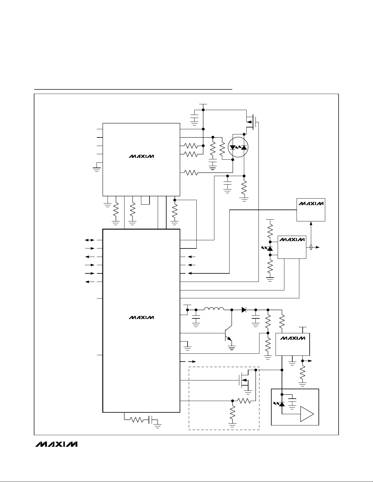
Typical Operating Circuit
PON Triplexer and SFP Controller
______________________________________________________________________________________ 15
I2C COMMUNICATION
FAULT OUTPUT
DISABLE INPUT
RECEIVER LOS
OPEN-DRAIN LOS OUTPUT
ADDITIONAL DIGITAL I/O
IN+
IN-
BEN+
BEN-
DIS
IMAX
GND
VMSET
MOD BIAS BEN
SDA
SCL
TX-F
TX-D
LOSI
D0
D3
MAX3643
MODSET
VREF
VBSET
BIASSET
M4DAC
V
CC
OUT+
OUT-
BIAS-
BIAS+
BENOUT
BCMON
BMD
MON1
MON2
MON3
MON4
FETG
D1
3.3V
3.3V
TRANSMIT POWER
RECEIVE POWER
CATV RF POWER
CATV SHUTDOWN CONTROL
MAX4003
MAX3654
FTTH CATV
TIA
RF DETECTOR
CATV
12V
GAIN CONTROL
ADDITIONAL MONITORS
MON[5:7]
COMP
DS1875
V
SW
GND
DAC1
MON8
CC
FB
APD OVERLOAD QUICK TRIP
D2
APD VOLTAGE MONITOR
VOLTAGE REFERENCE
OPTIONAL
R
AGC
MAX4007
CURRENT MONITOR
APD
3.3V
RECEIVE
POWER
(CURRENT)
ROSA
TIA
Page 16

DS1875
PON Triplexer and SFP Controller
16 ______________________________________________________________________________________
Detailed Description
The DS1875 integrates the control and monitoring functionality required to implement a PON system using
Maxim’s MAX3643 compact burst-mode laser driver.
The compact laser-driver solution offers a considerable
cost benefit by integrating control and monitoring features in the low-power CMOS process, while leaving
only the high-speed portions to the laser driver. Key
components of the DS1875 are shown in the
Block
Diagram
and described in subsequent sections. Table
1 contains a list of acronyms used in this data sheet.
Bias Control
Bias current is controlled by an APC loop. The APC
loop uses digital techniques to overcome the difficulties
associated with controlling burst-mode systems.
Autodetect Bias Control
This is the default mode of operation. In autodetect bias
control, transmit burst length is monitored. A “short
burst” is declared when the burst is shorter than
expected based on the sample rate setting in Table
02h, Register 88h. In the case that 32 consecutive short
bursts are transmitted, the integrator is disabled and
the BIAS DAC is loaded from the BIAS LUT (Table 08h).
Any single burst of adequate burst length re-enables
the APC integrator.
Open-Loop Bias Control
Open-loop control is configured by setting FBOL in
Table 02h, Register C7h. In this mode, the BIAS LUT
(Table 08h) is directly loaded to the BIAS DAC output.
The BIAS LUT can be programmed in 2°C increments
over the 40°C to +102°C range. It is left-shifted so that
the LUT value is loaded to either the DAC MSB or the
DAC MSB-1 (Bit BOLFS, Table 02h, Register 89h).
Closed-Loop Bias Control
The closed-loop control requires a burst length long
enough to satisfy the sample rate settings in Table 02h,
Register 88h (APC_SR[3:0]). Closed-loop control is
configured by setting FBCL in Table 02h, Register C7h.
In this mode, the APC integrator is enabled, which controls the BIAS DAC.
The APC loop begins by loading the value from the
BIAS LUT (Table 08h) indexed by the present temperature conversion. The feedback for the APC loop is the
monitor diode (BMD) current, which is converted to a
voltage using an external resistor. The feedback voltage is compared to an 8-bit scaleable voltage reference, which determines the APC set point of the
system. Scaling of the reference voltage accommodates the wide range in photodiode sensitivities. This
allows the application to take full advantage of the APC
reference’s resolution.
The DS1875 has an LUT to allow the APC set point to
change as a function of temperature to compensate for
TE. The TE LUT (Table 05h) has 36 entries that determine the APC setting in 4°C windows between -40°C to
+100°C. Ranging of the APC DAC is possible by programming a single byte in Table 02h, Register 8Dh.
Table 1. DS1875 Acronyms
ACRONYM DEFINITION
10GEPON 10-Gigabit Ethernet PON
ADC Analog-to-Digital Converter
AGC Automatic Gain Control
APC Automatic Power Control
APD Avalanche Photodiode
BM Burst Mode
BPON Broadband PON
CATV Cable Televis ion
EPON Ethernet PON
ER Extinction Ratio
DAC Digital-to-Analog Converter
FTTH Fiber-to-the-Home
FTTX Fiber-to-the-X
GEPON Gigabit Ethernet PON
GPON Gigabit PON
LOS Loss of Signal
LUT Lookup Table
TE Track ing Error
TIA Transimpedance Amplif ier
ROSA Receiver Optical Subassembly
RSSI Receive Signal Strength Indicator
PON Passive Optical Network
PWM Pulse-Width Modulation
SFF Small Form Factor
SFF-8472
SFP Small Form Factor Pluggable
SFP+ Enhanced SFP
TOSA Transmit Optical Subassembly
Document Defining Register Map of
SFPs and SFFs
Page 17
DS1875
DC Operation
When using autodetect mode or closed-loop mode,
BEN should be equal to VCCor long burst. In open-loop
mode, BEN should be ground or any burst length.
Modulation Control
The MOD output is an 8-bit scaleable voltage output
that interfaces with the MAX3643’s VMSET input. An
external resistor to ground from the MAX3643’s
MODSET pin sets the maximum current that the voltage
at the VMSET input can produce for a given output
range. This resistor value should be chosen to produce
the maximum modulation current the laser type requires
over temperature. Then the MOD output’s scaling is
used to calibrate the full-scale (FS) modulation output
to a particular laser’s requirements. This allows the
application to take full advantage of the MOD output’s
resolution. The modulation LUT can be programmed in
2°C increments over the -40°C to +102°C range.
Ranging of the MOD DAC is possible by programming
a single byte in Table 02h, Register 8Bh.
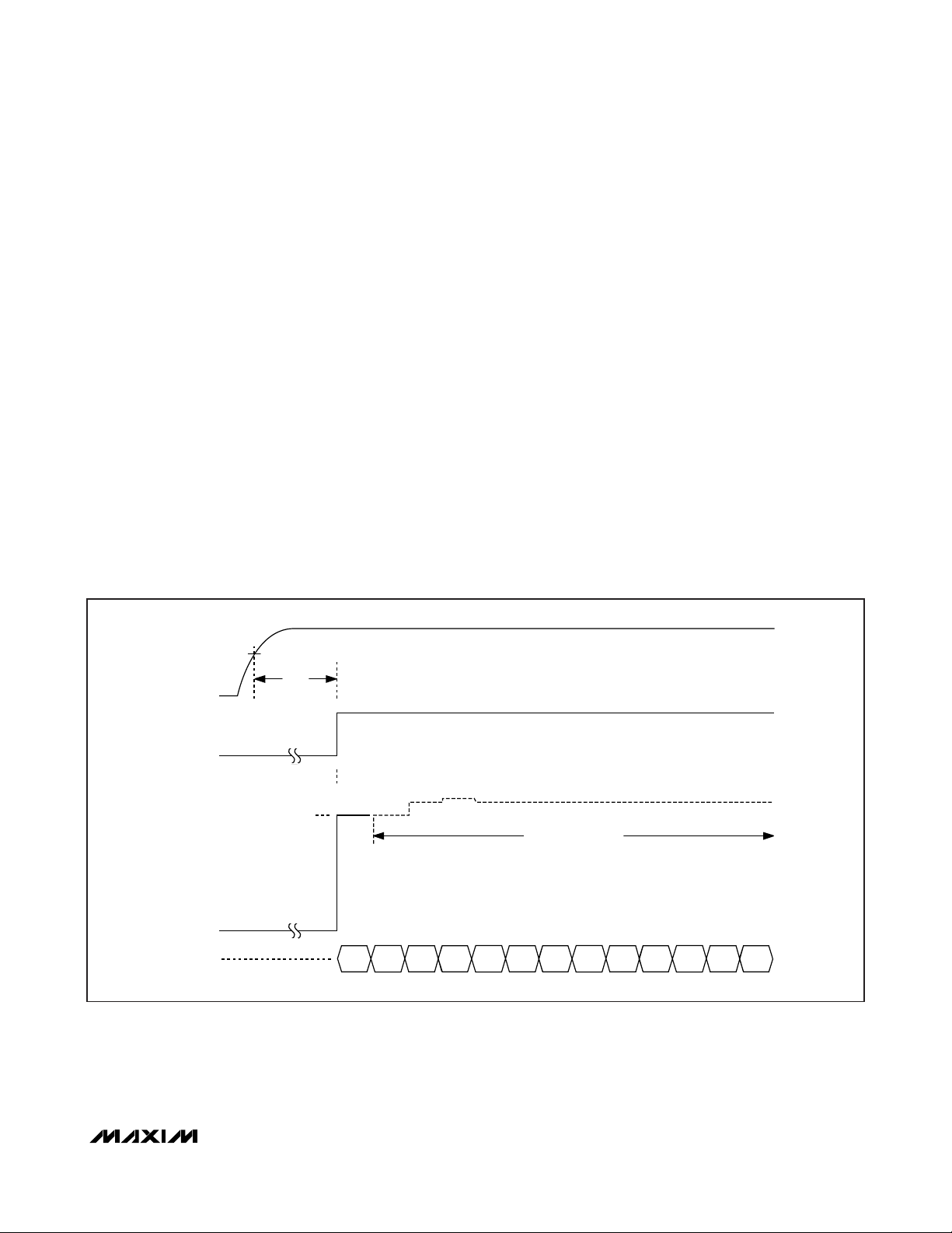
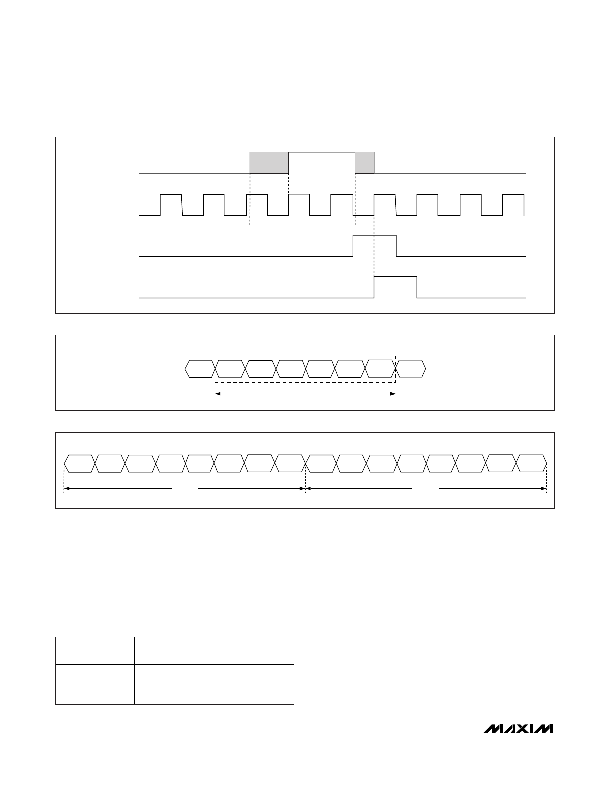
BIAS and MOD Output During Power-Up
On power-up the modulation and bias outputs remain off
until VCCis above V
POA
, a temperature conversion has
been completed, and, if the VCCADC alarm is enabled,
a V
CC
conversion above the customer-defined VCClow
alarm level must clear the VCClow alarm (t
INIT
). Once all
these conditions (t
INIT
) are satisfied, the MOD output is
enabled with the value determined by the temperature
conversion and the modulation LUT (Table 04h).
When the MOD output is enabled, the BIAS output is
turned on to a value equal to the temperature-indexed
value in the BIAS LUT (Table 08h). Next, the APC integrator is enabled, and single LSB steps are taken to
tightly control the average power.
If a fault is detected and TX-D is toggled to re-enable
the outputs, the DS1875 powers up following a similar
sequence to an initial power-up. The only difference is
that the DS1875 already determined the present temperature, so the t
INIT
time is not required for the
DS1875 to recall the APC and MOD set points from
EEPROM.
Figure 1. Power-Up Timing (BEN is a Long Burst)
PON Triplexer and SFP Controller
______________________________________________________________________________________ 17
V
V
CC
POA
t
INIT
V
MOD
BIAS LUT
VALUE
I
BIAS
BIAS
SAMPLE
12345678910111213
APC INTEGRATOR ON
Page 18
DS1875
PON Triplexer and SFP Controller
18 ______________________________________________________________________________________
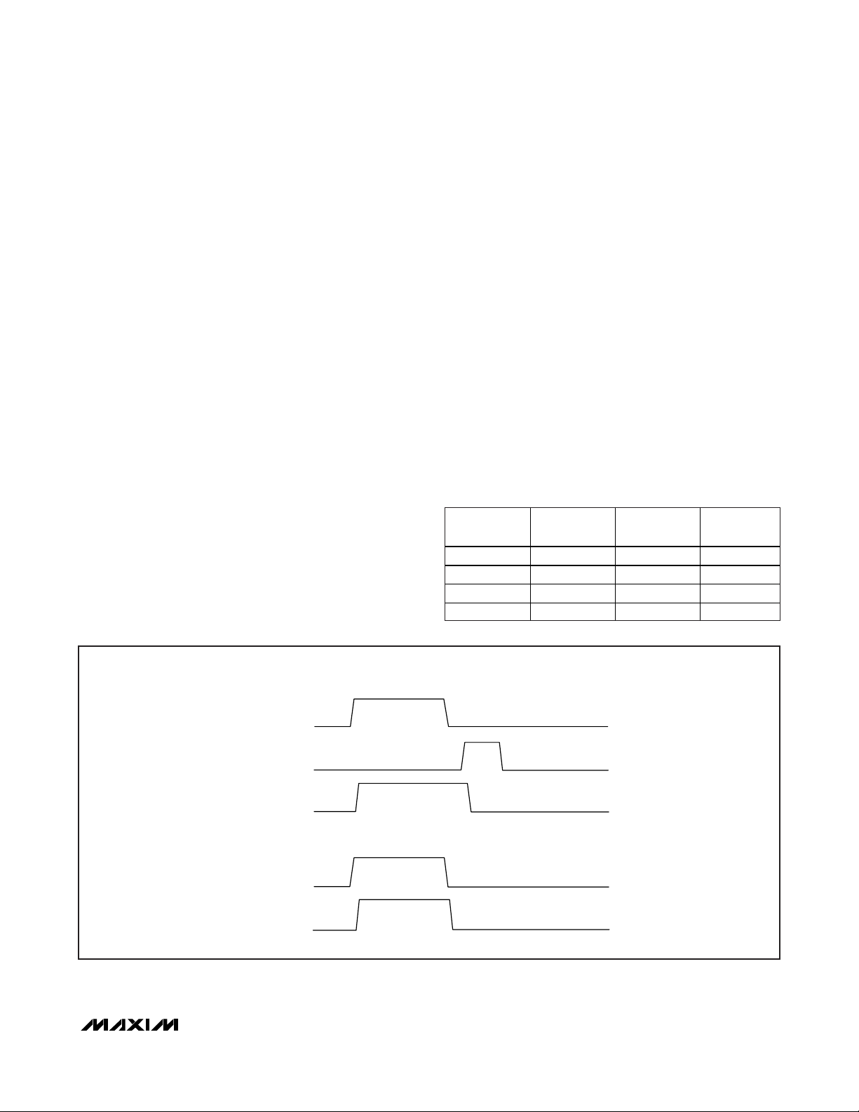
BIAS and MOD Output as a Function of
Transmit Disable (TX-D)
If the TX-D pin is asserted (logic 1) during normal operation, the outputs are disabled within t
OFF
. When TX-D
is deasserted (logic 0), the DS1875 turns on the MOD
output with the value associated with the present temperature and initializes the BIAS using the same search
algorithm used at startup. When asserted, the SOFT
TX-D bit (Lower Memory, Register 6Eh) offers a software control identical to the TX-D pin (see Figure 2).
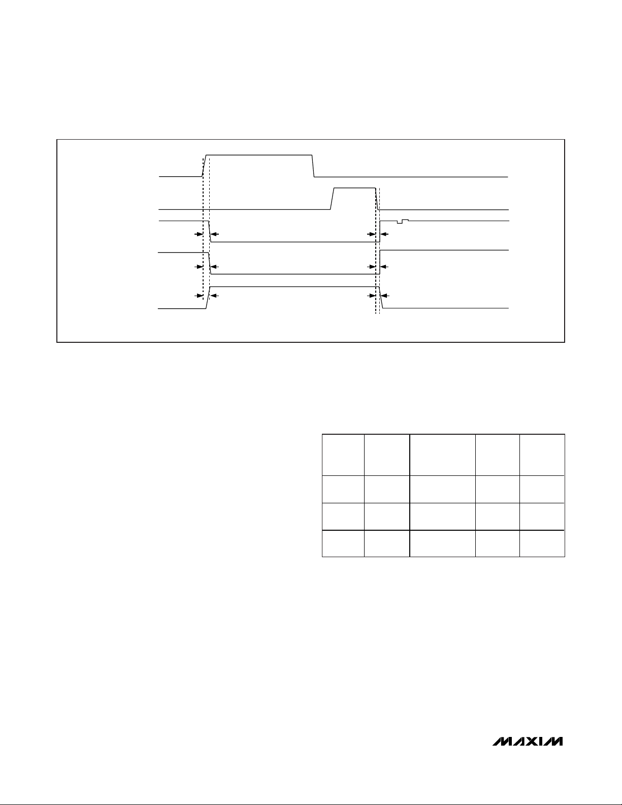
APC and Quick-Trip Shared Comparator
Timing
As shown in Figure 3, the DS1875’s input comparator is
shared between the APC control loop and the three
quick-trip alarms (TXP HI, TXP LO, and BIAS HI). The
comparator polls the alarms in a multiplexed sequence.
Six of every eight comparator readings are used for
APC loop-bias current control. The other two updates
are used to check the HTXP/LTXP (monitor diode voltage) and the HBIAS (MON1) signals against the internal APC and BIAS reference. If the last APC
comparison was higher than the APC set point, it
makes an HTXP comparison, and if it is lower, it makes
an LTXP comparison. Depending on the results of the
comparison, the corresponding alarms and warnings
(TXP HI, TXP LO) are asserted or deasserted.
The DS1875 has a programmable comparator sample
time based on an internally generated clock to facilitate
a wide variety of external filtering options suitable for
burst-mode transmitters. The rising edge of BEN triggers the sample to occur, and the Update Rate register
(Table 02h, Register 88h) determines the sampling time.
The first sample occurs (t
FIRST
) after the rising edge of
BEN. The internal clock is asynchronous to BEN, causing a ±50ns uncertainty regarding when the first sample
will occur following BEN. After the first sample occurs,
subsequent samples occur on a regular interval, t
REP
.
Table 2 shows the sample rate options available.
Updates to the TXP HI and TXP LO quick-trip alarms do
not occur during the BEN low time. The BIAS HI quick
trip can be sampled during the burst-low time. Any
*
All codes greater than 1001b (1010b to 1111b) use the
maximum sample time of code 1001b.
Figure 3. APC Loop and Quick-Trip Sample Timing
Table 2. Update Rate Timing
Figure 2. TX-D Timing
TX-D
I
BIAS
V
MOD
t
OFF
t
OFF
t
ON
t
ON
MINIMUM TIME
FROM BEN TO
APC_SR[3:0]
0000b 350 800
0001b 550 1200
0010b 750 1600
0011b 950 2000
0100b 1350 2800
0101b 1550 3200
0110b 1750 3600
0111b 2150 4400
1000b 2950 6000
1001b* 3150 6400
FIRST SAMPLE
(t
) ±50ns
FIRST
(ns)
REPEATED
SAMPLE PERIOD
FOLLOWING FIRST
SAMPLE (t
(ns)
REP
)
t
BEN
APC QUICK-TRIP
SAMPLE TIMES
FIRST
t
REP
APC
SAMPLE
APC
SAMPLE
APC
SAMPLE
APC
SAMPLE
APC
SAMPLE
APC
SAMPLE
HTXP/LTXP
SAMPLE
HBIAS
SAMPLE
APC
SAMPLE
Page 19

DS1875
quick-trip alarm that is detected by default remains
active until a subsequent comparator sample shows the
condition no longer exists. A second bias-current monitor (BIAS MAX) compares the DS1875’s BIAS DAC’s
code to a digital value stored in the MAX BIAS register.
This comparison is made at every bias-current update
to ensure that a high bias current is quickly detected.
Monitors and Fault Detection
Monitors
Monitoring functions on the DS1875 include a power-on
analog (POA) VCCcomparison, five quick-trip comparators, and ADC channels. This monitoring combined
with the interrupt masks determine if the DS1875 shuts
down its outputs and triggers the TX-F and FETG outputs. All the monitoring levels and interrupt masks are
user programmable with the exception of POA, which
trips at a fixed range and is nonmaskable for safety
reasons.
Power-On Analog (POA)
POA holds the DS1875 in reset until VCCis at a suitable
level (VCC> V
POA
) for the part to accurately measure
with its ADC and compare analog signals with its quicktrip monitors. Because VCCcannot be measured by the
ADC when VCCis less than V
POA
, POA also asserts the
VCClow alarm, which is cleared by a VCCADC conversion greater than the customer-programmable VCClow
ADC limit. This allows a programmable limit to ensure
that the head room requirements of the transceiver are
satisfied during slow power-up. The TX-F and FETG
outputs do not latch until there is a conversion above
the VCClow limit. The POA alarm is nonmaskable. The
TX-F and FETG outputs are asserted when VCCis
below V
POA
. See the
Low-Voltage Operation
section for
more information.
Five Quick-Trip Monitors and Alarms
Five quick-trip monitors are provided to detect potential
laser safety issues. These monitor:
1) High Bias Current (HBIAS)
2) Low Transmit Power (LTXP)
3) High Transmit Power (HTXP)
4) Max Output Current (BIAS MAX)
5) MON3 Quick Trip (M3QT)
The high- and low-transmit power quick-trip registers
(HTXP and LTXP) set the thresholds used to compare
against the BMD voltage to determine if the transmit
power is within specification. The HBIAS quick trip compares the MON1 input (generally from the MAX3643
bias monitor output) against its threshold setting to
determine if the present bias current is above specifica-
tion. The BIAS MAX quick trip is a digital comparison
that determines if the BIAS DAC indicates that the bias
current is above specification. I
BIAS
is not allowed to
exceed the value set in the MAX BIAS register. When
the DS1875 detects that the bias is at the limit, it sets
the BIAS MAX status bit and clamps the bias current at
the MAX BIAS level. In the closed-loop mode, if the
recalled value from the BIAS LUT is greater than MAX
BIAS then, the update is not done and I
BIAS
reverts to
the previous I
BIAS
value. The quick trips are routed to
the TX-F and FETG outputs through interrupt masks to
allow combinations of these alarms to be used to trigger
these outputs. When FETG is triggered, the DS1875 also
disables the MOD and BIAS outputs. See the
BIAS and
MOD Output During Power-Up
section for details.
MON3 Quick Trip
One additional quick trip is used to protect the APD
from overcurrent. MON3P is used to monitor the current
through the APD. When MON3P exceeds a threshold
set by the M3QT DAC register (Table 02h, Register
C3h), the PWM is shut down by blocking SW pulses.
The MON3 comparison is single-ended referenced to
ground. In the case where MON3 is used differentially
and not referenced to ground, this must be considered
when setting the MON3 quick-trip threshold.
Additionally, the D2 pin can be driven either high or low
as determined by INV M3QT and MUX M3QT bits in
Lower Memory, Register 79h. An external switch controlled by pin D2 may be used to clamp the converter’s
output when MON3 quick trip occurs. This external
switch discharges the output voltage much faster than
allowing the load to discharge the rail. The MON3
quick-trip alarm can be latched by enabling M3QT LEN
in Table 02h, Register 89h. The latch is reset by setting
M3QT RESET in Lower Memory, Register 78h. A soft
quick trip is performed by setting SOFT M3QT in Lower
Memory, Register 78h (see Figure 4).
ADC Monitors and Alarms
The ADC monitors six channels that measure temperature (internal temp sensor), VCC, and MON1–MON4
using an analog multiplexer to measure them round
robin with a single ADC. Each channel has a customerprogrammable full-scale range and offset value that is
factory programmed to default value (see Table 3).
Additionally, MON1–MON4 can right-shift results by up
to 7 bits before the results are compared to alarm
thresholds or read over the I2C bus. This allows customers with specified ADC ranges to calibrate the ADC
full scale to a factor of 1/2ntheir specified range to
measure small signals. The DS1875 can then right-shift
the results by n bits to maintain the bit weight of their
specification.
PON Triplexer and SFP Controller
______________________________________________________________________________________ 19
Page 20
DS1875
PON Triplexer and SFP Controller
20 ______________________________________________________________________________________
The ADC results (after right-shifting, if used) are compared to high and low alarm and warning thresholds
after each conversion. The alarm values can be used to
trigger the TX-F or FETG outputs. These ADC thresholds
are user programmable through the I2C interface, as
well as masking registers that can be used to prevent
the alarms from triggering the TX-F and FETG outputs.
ADC Timing
There are 10 analog channels that are digitized in a
sequential fashion. The MON5–MON8 channels are
sampled depending on the state of the EN5TO8B bit in
Table 02h, Register 89h. If the bit is programmed to
logic 0, the ADC cycles through temperature, VCC, and
MON1–MON4 (Figure 5). If the bit is programmed to
logic 1, all 10 channels are digitized, including channels MON5–MON8 (Figure 6). In this mode (EN5TO8B
= 0), each of MON5–MON8 is sampled on alternate
cycles, as shown in Figure 5. The total time required to
convert one set of channels is the sequential ADC
cycle time, t
FRAME1
or t
FRAME2
(see Figure 6).
Table 3. ADC Default Monitor Ranges
Figure 6. ADC Timing with EN5TO8B = 1
Figure 5. ADC Timing with EN5TO8B = 0
Figure 4. M3QT Timing
TRIP CONDITION
mCLK
(525kHz)
CAPTURE ALARM
M3QT ALARM
(UNLATCHED)
ONE ADC CYCLE
MON4
TEMP
V
CC
MON1
V
CC
MON2 MON3 MON4
t
FRAME2
MON5 MON6TEMP V
SIGNAL
+FS
SIGNAL
Temperature (°C) 127.996 7FFF -128 8000
VCC (V) 6.5528 FFF8 0 0000
MON1–MON8 (V) 2.4997 FFF8 0 0000
+FS
HEX
-FS
SIGNAL
-FS
HEX
MON1 MON2 MON3 MON4 TEMP
t
FRAME1
MON1
CC
MON2 MON3 MON4
t
FRAME2
MON7 MON8TEMP
Page 21
DS1875
Right-Shifting ADC Result
If the weighting of the ADC digital reading must conform to a predetermined full-scale value defined by a
standard’s specification, then right-shifting can be used
to adjust the predetermined full-scale analog measurement range while maintaining the weighting of the ADC
results. The DS1875’s range is wide enough to cover all
requirements; when the maximum input value is ≤ 1/2
the FS value, right-shifting can be used to obtain
greater accuracy. For instance, the maximum voltage
might be 1/8th the specified predetermined full-scale
value, so only 1/8th the converter’s range is used. An
alternative is to calibrate the ADC’s full-scale range to
1/8th the readable predetermined full-scale value and
use a right-shift value of 3. With this implementation, the
resolution of the measurement is increased by a factor
of 8, and because the result is digitally divided by 8 by
right-shifting, the bit weight of the measurement still
meets the standard’s specification (i.e., SFF-8472).
The right-shift operation on the ADC result is carried out
based on the contents of RIGHT SHIFT1/0 registers
(Table 02h, Registers 8Eh–8Fh). Four analog channels,
MON1–MON4, have 3 bits each allocated to set the
number of right-shifts. Up to seven right-shift operations
are allowed and are executed as a part of every conversion before the results are compared to the high and
low alarm levels, or loaded into their corresponding
measurement registers (Table 01h, Registers
62h–6Bh). This is true during the setup of internal calibration as well as during subsequent data conversions.
Transmit Fault (TX-F) Output
The TX-F output has masking registers for the ADC
alarms and the QT alarms to select which comparisons
cause it to assert. In addition, the FETG alarm is selectable through the TX-F mask to cause TX-F to assert. All
alarms, with the exception of FETG, only cause TX-F to
remain active while the alarm condition persists.
However, the TX-F latch bit can enable the TX-F output
to remain active until it is cleared by the TX-F reset bit,
TX-D, SOFT TX-D, or by power cycling the part. If the
FETG output is configured to trigger TX-F, it indicates
that the DS1875 is in shutdown and requires TX-D,
SOFT TX-D, or cycling power to reset. Only enabled
alarms activate TX-F (see Figure 7). Table 4 shows
TX-F as a function of TX-D and the alarm sources.
Table 4. TX-F as a Function of TX-D and
Alarm Sources
Figure 7. TX-F Timing
PON Triplexer and SFP Controller
______________________________________________________________________________________ 21
VCC > V
POA
No X X 1
Yes 0 0 0
Yes 0 1 1
Yes 1 X 0
TX-D
NONMASKED
TX-F ALARM
TX-F
TX-F LATCHED OPERATION
DETECTION OF
TX-F FAULT
TX-D OR
TX-F RESET
TX-F
TX-F NONLATCHED OPERATION
DETECTION OF
TX-F FAULT
TX-F
Page 22
DS1875
PON Triplexer and SFP Controller
22 ______________________________________________________________________________________
Safety Shutdown (FETG) Output
The FETG output has masking registers (separate from
TX-F) for the ADC alarms and the QT alarms to select
which comparisons cause it to assert. Unlike TX-F, the
FETG output is always latched. Its output polarity is
programmable to allow an external nMOS or pMOS to
open during alarms to shut off the laser-diode current.
If the FETG output triggers, indicating that the DS1875
is in shutdown, it requires TX-D, SOFT TX-D, or cycling
power to be reset. Under all conditions, when the analog outputs are reinitialized after being disabled, all the
alarms with the exception of the VCClow ADC alarm
are cleared. The VCClow alarm must remain active to
prevent the output from attempting to operate when
inadequate VCCexists to operate the laser driver. Once
adequate VCCis present to clear the VCClow alarm,
the outputs are enabled following the same sequence
as the power-up sequence.
As previously mentioned, the FETG is an output used to
disable the laser current through a series nMOS or
pMOS. This requires that the FETG output can sink or
source current. Because the DS1875 does not know if it
should sink or source current before VCCexceeds
V
POA
, which triggers the EE recall, this output is high
impedance when VCCis below V
POA
(see the
Low-
Voltage Operation
section for details and diagram). The
application circuit should use a pullup or pulldown
resistor on this pin that pulls FETG to the alarm/shutdown state (high for a pMOS, low for a nMOS). Once
VCCis above V
POA
, the DS1875 pulls the FETG output
to the state determined by the FETG DIR bit (Table 02h,
Register 89h). Set FETG DIR to 0 if an nMOS is used
and 1 if a pMOS is used.
Determining Alarm Causes Using the I2C
Interface
To determine the cause of the TX-F or FETG alarm, the
system processor can read the DS1875’s alarm trap bytes
(ATB) through the I2C interface (Table 01h, Registers
F8h–FBh). The ATB has a bit for each alarm. Any time an
alarm occurs, regardless of the mask bit’s state, the
DS1875 sets the corresponding bit in the ATB. Active ATB
bits remain set until written to 0s through the I2C interface.
On power-up, the ATB is 0s until alarms dictate otherwise.
FETG causes additional alarms that make it difficult to
determine the root cause of the problem. Therefore, no
updates are made to the ATB when FETG occurs.
Figure 8. FETG/Output Disable Timing (Fault Condition Detected)
Table 5. FETG, MOD, and BIAS Outputs
as a Function of TX-D and Alarm Sources
DETECTION OF
FETG FAULT
TX-D
I
BIAS
V
MOD
FETG*
*FETG DIR = 0
t
OFF
t
OFF
t
FETG:ON
t
ON
t
ON
t
FETG:OFF
VCC >
V
POA
Yes 0 0
Yes 0 1
Yes 1 X
TX-D
NONMASKED
FETG ALARM
FETG
FETG
DIR
FETG
DIR
FETG
DIR
MOD AND
BIAS
OUTPUTS
Enabled
Disabled
Disabled
Page 23
DS1875
Die Identification
The DS1875 has an ID hard-coded to its die. Two registers (Table 02h, Registers 86h–87h) are assigned for
this feature. Byte 86h reads 75h to identify the part as
the DS1875; byte 87h reads the die revision.
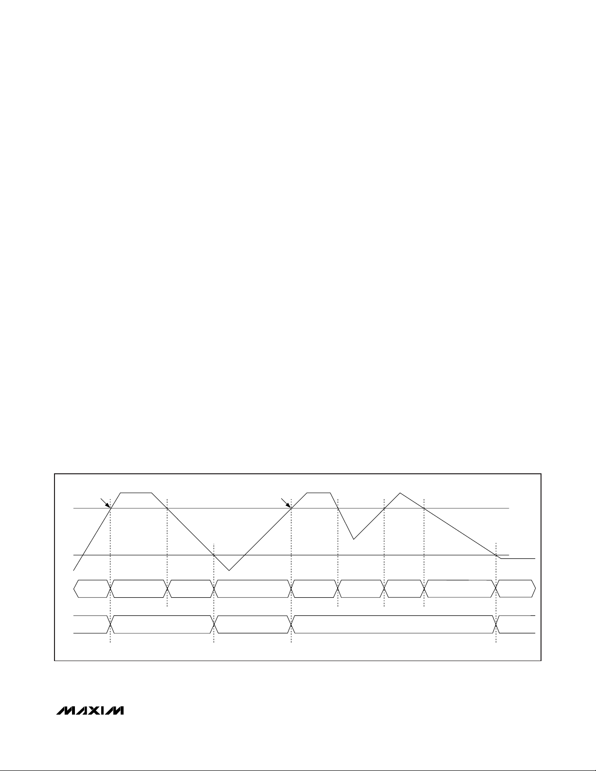
Low-Voltage Operation
The DS1875 contains two power-on reset (POR) levels.
The lower level is a digital POR (V
POD
) and the higher
level is an analog POR (V
POA
). At startup, before the
supply voltage rises above V
POA
, the outputs are disabled (FETG and BIAS outputs are high impedance,
MOD is low), all SRAM locations are low (including
shadowed EEPROM (SEE)), and all analog circuitry is
disabled. When VCCreaches V
POA
, the SEE is
recalled, and the analog circuitry is enabled. While V
CC
remains above V
POA
, the device is in its normal operating state, and it responds based on its nonvolatile configuration. If during operation VCCfalls below V
POA
but
is still above V
POD
, the SRAM retains the SEE settings
from the first SEE recall, but the device analog is shut
down and the outputs are disabled. FETG is driven to
its alarm state defined by the FETG DIR bit (Table 02h,
Register 89h). If the supply voltage recovers back
above V
POA
, the device immediately resumes normal
functioning. When the supply voltage falls below V
POD
,
the device SRAM is placed in its default state and
another SEE recall is required to reload the nonvolatile
settings. The EEPROM recall occurs the next time V
CC
exceeds V
POA
. Figure 9 shows the sequence of events
as the voltage varies.
Any time V
CC
is above V
POD
, the I2C interface can be
used to determine if VCCis below the V
POA
level. This
is accomplished by checking the RDYB bit in the status
(Lower Memory, Register 6Eh) byte. RDYB is set when
VCCis below V
POA
. When VCCrises above V
POA
,
RDYB is timed (within 500µs) to go to 0, at which point
the part is fully functional.
For all device addresses sourced from EEPROM (Table
02h, Register 8Ch), the default device address is A2h
until VCCexceeds V
POA
, allowing the device address
to be recalled from the EEPROM.
Enhanced RSSI Monitoring (Dual Range
Functionality)
The DS1875 offers a new feature to improve the accuracy and range of MON3, which is most commonly
used for monitoring RSSI. This feature enables rightshifting (along with its gain and offset settings) when
the input signal is below a set threshold (within the
range that benefits using right-shifting) and then automatically disables right-shifting (recalling different gain
and offset settings) when the input signal exceeds the
threshold. Also, to prevent “chattering,” hysteresis prevents excessive switching between modes in addition
to ensuring that continuity is maintained. Dual range
operation is enabled by default (factory programmed in
EEPROM). However, it can easily be disabled through
the RSSI_FF and RSSI_FC bits. When dual range operation is disabled, MON3 operates identically to the
other MON channels, although featuring a differential
input.
Figure 9. SEE Timing
PON Triplexer and SFP Controller
______________________________________________________________________________________ 23
SEE RECALL SEE RECALL
V
POA
V
CC
V
POD
HIGH
FETG
IMPEDANCE
PRECHARGED
SEE
TO 0
HIGH
IMPEDANCE
PRECHARGED
TO 0
RECALLED
VALUE
DRIVEN TO
FETG DIR
NORMAL
OPERATION
NORMAL
OPERATION
DRIVEN TO
FETG DIR
OPERATION
RECALLED
VALUE
NORMAL
DRIVEN TO
FETG DIR
HIGH
IMPEDANCE
PRECHARGED
TO 0
Page 24
DS1875
24 ______________________________________________________________________________________
Dual-range functionality consists of two modes of operation: fine mode and coarse mode. Each mode is calibrated for a unique transfer function, hence the term, dual
range. Table 6 highlights the registers related to MON3.
Fine mode is equivalent to the other MON channels. Fine
mode is calibrated using the gain, offset, and right-shifting registers at locations shown in Table 6 and is ideal
for relatively small analog input voltages. Coarse mode is
automatically switched to when the input exceeds the
threshold (to be discussed in a subsequent paragraph).
Coarse mode is calibrated using different gain and offset
registers, but lacks right-shifting (since coarse mode is
only used on large input signals). The gain and offset
registers for coarse mode are also shown in Table 6.
With the use of right-shifting, the fine mode full scale is
programmed to (1/2N)th the coarse mode full scale. The
DS1875 will now autorange to choose the range that
gives the best resolution for the measurement. To eliminate chatter, 6.25% of hysteresis is applied when the
input resides at the boundary of the two ranges. See
Figure 10. Additional information for each of the registers
can be found in the
Memory Map
section.
Dual range operation is transparent to the end user. The
results of MON3 analog-to-digital conversions are still
stored/reported in the same memory locations (68–69h,
Lower Memory) regardless of whether the conversion
was performed in fine mode or coarse mode.
When the DS1875 is powered up, analog-to-digital conversions begin in a round-robin fashion. Every MON3
timeslice begins with a fine mode analog-to-digital conversion (using fine mode’s gain, offset, and right-shifting settings). See the flowchart in Figure 10. Then,
depending on whether the last MON3 timeslice resulted
in a coarse-mode conversion and also depending on
the value of the current fine conversion, decisions are
made whether to use the current fine-mode conversion
result or to make an additional conversion (within the
same MON3 timeslice), using coarse mode (using
coarse mode’s gain and offset settings, and no rightshifting) and reporting the coarse-mode result. The
flowchart also illustrates how hysteresis is implemented. The fine-mode conversion is compared to one of
Figure 10. RSSI Flowchart
Table 6. MON3 Configuration Registers
PON Triplexer and SFP Controller
MON3
TIMESLICE
PERFORM FINE-
MODE CONVERSION
DID PRIOR MON3
TIMESLICE RESULT IN A
COARSE CONVERSION?
(LAST RSSI = 1?)
DID CURRENT FINEMODE CONVERSION
REACH MAX?
LAST RSSI = 0
REPORT FINE
CONVERSION RESULT
END OF MON3
TIMESLICE
Y
N
Y
N
N
WAS CURRENT FINE-
MODE CONVERSION
≥ 93.75% OF FS?
Y
PERFORM COARSE-
MODE CONVERSION
LAST RSSI = 1
REPORT COARSE
CONVERSION RESULT
REGISTER FINE MODE COARSE MODE
MON3 FINE SCALE 98h–99h, Table 02h 9Ch –9Dh, Table 02h
MON3 FINE OFFSET A8h–A9h, Table 02h ACh–ADh, Table 02h
RIGHT SHIFT0/1 8Eh–8Fh, Table 02h —
CONFIG (RSSI_FC, RSSI_FF bits) 89h, Table 02h
MON3 VALUE 68h–69h, Lower Memory
Page 25
DS1875
two thresholds. The actual threshold values are a function of the number of right-shifts being used. Table 7
shows the threshold values for each possible number
of right-shifts.
The RSSI_FF and RSSI_FC (Table 02h, Register 89h)
bits are used to force fine-mode or coarse-mode conversions, or to disable the dual-range functionality.
Dual-range functionality is enabled by default (both
RSSI_FC and RSSI_FF are factory programmed to 0 in
EEPROM). It can be disabled by setting RSSI_FC to 0
and RSSI_FF to 1. These bits are also useful when calibrating MON3. For additional information, see the
Memory Map
section.
PWM Controller
The DS1875 has a PWM controller that, when used with
external components, generates a low-noise, high-voltage output to bias APDs in optical receivers. The
achievable boost voltage is determined by the external
component selection. Figure 12 shows a typical
schematic. Selection of switching frequency, external
inductor, capacitors, resistor network, switching FET,
and switch diode determine the performance of the
DC-DC converter. The PWM controller can be configured in boost or buck mode. Both modes require an
external nMOS or npn transistor.
The DS1875 PWM controller consists of several sections used to create a PWM signal to drive a DC-DC
converter. Figure 11 is a block diagram of the DS1875
PWM controller. Following is a description of each
block in the PWM controller and some guidelines for
selecting components for the DC-DC converter.
The PWM DAC is used to set the desired output voltage
of the DC-DC converter section. The feedback from the
DC-DC converter is compared to the output from the
PWM DAC by an error amplifier. If the FB level is less
Table 7. MON3 Hysteresis Threshold Values
*
This is the minimum reported coarse-mode conversion.
Figure 11. PWM Controller Diagram
PON Triplexer and SFP Controller
______________________________________________________________________________________ 25
NO. OF RIGHT-
SHIFTS
0 FFF8h F000h
1 7FFCh 7800h
2 3FFEh 3C00h
3 1FFFh 1E00h
4 0FFFh 0F00h
5 07FFh 0780h
6 03FFh 03C0h
7 01FFh 01E0h
FINE MODE
(MAX)
COARSE MODE
(MIN*)
PWM EN
PWM DAC TEMPERATURE-
REFERENCED LUT
TABLE 07h
2
MANUAL I
C CONTROL
DS1875
PWM CONTROLLER
MUX
PWM DAC
TABLE 02h
REGISTER FEh
PWM_FR[1:0]
PWM DAC
8-BIT
0 TO 1.25V
RAMP
90% DUTY
CYCLE OSC
10μA
AMPLIFIER
10μA
ERROR
VOLTAGE CLAMP
HIGH = 2.1V
LOW = 0.8V
1.9V
1.0V
M3QT
GATE DRIVER
90% MAX
DUTY CYCLE
COMP
SW
FB
Page 26

DS1875
PON Triplexer and SFP Controller
26 ______________________________________________________________________________________
than the PWM DAC level, the error amplifier increases
the level on the COMP pin. The level on the COMP pin
is compared to the signal from the oscillator and ramp
generator to set the duty cycle that is input to the gate
driver and maximum duty-cycle limiting block. An
increase on the COMP pin increases the duty cycle.
Conversely, if FB is greater than the PWM DAC, the
level on COMP is decreased, decreasing the duty
cycle. The gate driver and maximum duty-cycle block
is used to limit the maximum duty cycle of the PWM
controller to 90%. This block also disables the PWM driver if an M3QT has resulted from the APD current
exceeding a desired limit.
The output from the PWM DAC is used to control the
output voltage of the DC-DC converter. The values for
the PWM DAC are recalled from the Table 07h, which is
a temperature-indexed LUT. The temperature-indexed
value from the LUT is written to the PWM DAC register
(Table 02h, Register FEh), which updates the setting of
the PWM DAC. The PWM DAC can also be operated in
a manual mode by disabling the automatic updating
from the LUT. This is done by clearing the PWM EN bit
(Table 02h, Register 80h, Bit 5). The PWM DAC fullscale output is 1.25V with 8 bits of resolution. When
designing the feedback for the DC-DC converter section, the user needs to make sure that the desired level
applied to the FB pin is in this range.
The COMP pin is driven by the error amplifier comparing the PWM DAC to the DC-DC converter feedback
signal at the FB pin. The error amplifier can sink and
source 10µA. An external resistor and capacitor connected to the COMP pin determine the rate of change
the COMP pin. The resistor provides an initial step
when the current from the error amplifier changes. The
capacitor determines how quickly the COMP pin
charges to the desired level. The COMP pin has internal voltage clamps that limit the voltage level to a minimum of 0.8V and a maximum of 2.1V.
The oscillator and ramp generator create a ramped signal. The frequency of this signal can be 131.25kHz,
262.5kHz, 525kHz, or 1050kHz and is set by the
PWM_FR[1:0] bits (Table 02h, Register 88h, Bits 5:4).
The low level and high level for the ramped signal are
approximately 1.0V and 1.9V, respectively.
The ramped signal is compared to the voltage level on
the COMP pin to determine the duty cycle that is input
to the gate driver and duty-cycle limiting block. When
COMP is clamped low at 0.8V, below the level of the
ramped signal, the comparator outputs a 0% dutycycle signal to the gate driver block. When COMP is
clamped at 2.1V, above the level of the ramped signal,
the comparator outputs a 100% duty-cycle signal to the
gate driver and duty-cycle limiting block. The dutycycle liming block is used to limit the duty cycle of the
PWM signal from the SW pin to 90%.
The PWM controller is designed to protect expensive
APDs against adverse operating conditions while providing optimal bias. The PWM controller monitors photodiode current to protect APDs under avalanche
conditions using the MON3 quick trip. A voltage level
that is proportional to the APD current can be input to
the MON3 pin. When this voltage exceeds the level set
by the M3QT DAC (Table 02h, Register C3h), pulses
from the PWM controller are blocked until the fault is
cleared. The quick trip can also toggle the digital output
D2. D2 can be connected to an external FET to quickly
discharge the DC-DC converter filter capacitors.
Inductor Selection
Optimum inductor selection depends on input voltage,
output voltage, maximum output current, switching frequency, and inductor size. Inductors are typically specified by their inductance (L), peak current (IPK), and
resistance (LR).
The inductance value is given by:
Where:
VIN= DC-DC converter input voltage
V
OUT
= Output of DC-DC converter
I
OUT(MAX)
= Maximum output current delivered
T = Time period of switching frequency (seconds)
D = Duty cycle
η = Estimated power conversion efficiency
The equation for inductance factors in conversion efficiency. For inductor calculation purposes, an η of 0.5
to 0.75 is usually suitable.
For example, to obtain an output of 80V with a load current of 1.0mA from an input voltage of 5.0V using the
maximum 90% duty cycle and frequency of 1050kHz
(T = 952ns), and assuming an efficiency of 0.5, the previous equation yields an L of 120µH, so a 100µH inductor would be a suitable value.
The peak inductor current is given by:
L
22
VDT
×××
IN
=
2
IV
OUT MAX OUT
()
VDT
××
PK
IN
=
L
I
η
×
Page 27

DS1875
Stability and Compensation Component Selection
The components connected to the COMP pin (R
COMP
and C
COMP
) introduce a pole and zero that are necessary for stable operation of the PWM controller
(Figure 12).
The dominant pole, POLE1, is formed by the output
impedance of the error amplifier (REA) and C
COMP
. The
zero formed by the components on COMP, ZERO1, is
selected to cancel POLE2 formed by the output filter
cap C3 and output load R
LOAD
. The additional pole,
POLE3, formed by R1 and C3 should be at least a
decade past the crossover frequency to not affect stability. The following formulas can be used to calculate
the poles and zero for the application shown in
Figure 12.
POLE1 (dominant pole) = 1/(2π × REA× C
COMP
)
ZERO1 (compensation zero) = 1/(2π × R
COMP
× C
COMP
)
POLE2 (output load pole) =
POLE3 (output filter pole) = 1/(2π × R1 × C3)
The DC open-loop gain is given by:
Where:
REA= 260MΩ
GM= 425µS
R
LOAD
= Parallel combination of feedback network and
load resistance
V
OUT
= Output of DC-DC converter
VIN= DC-DC converter input voltage
VFB= Feedback voltage at the FB pin
T = Time period of switching frequency (seconds)
L = Inductor value (henries)
DAC1 Output
The DAC1 output has a full-scale 2.5V range with 8 bits
of resolution, and is programmed through the I2C interface. The DAC1 setting is nonvolatile and password-2
(PW2) protected.
M4DAC Output
The M4DAC output has a full-scale 2.5V range with 8
bits of resolution, and is controlled by an LUT indexed
by the MON4 voltage. The M4DAC LUT (Table 06h) is
nonvolatile and PW2 protected. See the
Memory
Organization
section for details. The recalled value is
either 16-bit or 32-bit depending on bits DBL_SB and
UP_LOWB in Table 02h, Register C7h.
Digital I/O Pins
Five digital I/O pins are provided for additional monitoring and control. By default the LOSI pin is used to convert a standard comparator output for loss of signal
(LOSI) to an open-collector output. This means the mux
shown on the block diagram by default selects the LOSI
pin as the source for the D0 output transistor. The level
of the D0 pin can be read in the STATUS byte (Lower
Memory, Register 6Eh) as the LOS STATUS bit. The
LOS STATUS bit reports back the logic level of the D0
pin, so an external pullup resistor must be provided for
this pin to output a high level. The LOSI signal can be
inverted before driving the open-drain output transistor
using the XOR gate provided. The MUX LOS allows the
D0 pin to be used identically to the D1, D2, and D3
pins. However, the mux setting (stored in the EEPROM)
does not take effect until VCC> V
POA
, allowing the EEPROM to recall. This requires the LOSI pin to be grounded for D0 to act identical to the D1, D2, and D3 pins.
Digital pins D1, D2, and D3 can be used as inputs or
outputs. External pullup resistors must be provided to
realize high-logic levels. The DIN byte indicates the
logic levels of these input pins (Lower Memory, Register
79h), and the open-drain outputs can be controlled
using the DOUT byte (Lower Memory, Register 78h).
When VCC< V
POA
, these outputs are high impedance.
Once VCC≥ V
POA
, the outputs go to the power-on
default state stored in the DPU byte (Table 02h, Register
C0h). The EEPROM-determined default state of the pin
can be modified with PW2 access. After the default
state has been recalled, the SRAM registers controlling
outputs can be modified without password access. This
allows the outputs to be used to control serial interfaces
without wearing out the default EEPROM setting.
D2 can be configured as the output of a quick-trip monitor for MON3. The main application is to quickly shut
down the PWM converter and discharge the voltage
created by the converter. This is shown in the typical
application circuit.
PON Triplexer and SFP Controller
______________________________________________________________________________________ 27
2
×−
VV
OUT IN
−
VV R CC
OUT IN LOAD
×
223
××+
π
1
()
AOL G R
=× × ×
MEA
VV
FB IN
08522.
×
VV
×−
OUT IN
×
⎜
⎝
−
VV
OUT IN
VV
OUT
×
×
RT
LOAD
×
2
L
⎛
⎞
⎟
⎠
Page 28
DS1875
PON Triplexer and SFP Controller
28 ______________________________________________________________________________________
Figure 14. PWM Controller Current-Sink Output Configuration
Figure 13. PWM Controller Voltage Output Configuration
Figure 12. PWM Controller Typical APD Bias Circuit
V
SW
IN
L1
C1
D1
Q1
R1
C2
FB
C
COMP
R
COMP
COMP
V
OUT
C3
R2
R3
R4
MAX4007
3.3V
RMON
DS1875
APD OVERLOAD QUICK TRIP
D2
MON3
VOLTAGE OUTPUT
DS1875
SW
FB
COMP
DS1875
SW
COMP
FB
APD
C4
ROSA
TIA
CURRENT SINK
Page 29

DS1875
Figure 15. I2C Timing Diagram
I
2
C Communication
I2C Definitions
The following terminology is commonly used to
describe I
2
C data transfers.
Master Device: The master device controls the
slave devices on the bus. The master device generates SCL clock pulses and START and STOP conditions.
Slave Devices: Slave devices send and receive
data at the master’s request.
Bus Idle or Not Busy: Time between STOP and
START conditions when both SDA and SCL are inactive and in their logic-high states.
START Condition: A START condition is generated
by the master to initiate a new data transfer with a
slave. Transitioning SDA from high to low while SCL
remains high generates a START condition. See
Figure 15 for applicable timing.
STOP Condition: A STOP condition is generated by
the master to end a data transfer with a slave.
Transitioning SDA from low to high while SCL
remains high generates a STOP condition. See
Figure 15 for applicable timing.
Repeated START Condition: The master can use a
repeated START condition at the end of one data
transfer to indicate that it will immediately initiate a
new data transfer following the current one.
Repeated START conditions are commonly used
during read operations to identify a specific memory
address to begin a data transfer. A repeated START
condition is issued identically to a normal START
condition. See Figure 15 for applicable timing.
Bit Write: Transitions of SDA must occur during the
low state of SCL. The data on SDA must remain valid
and unchanged during the entire high pulse of SCL
plus the setup and hold-time requirements (Figure
15). Data is shifted into the device during the rising
edge of the SCL.
Bit Read: At the end of a write operation, the master
must release the SDA bus line for the proper amount
of setup time before the next rising edge of SCL during a bit read (Figure 15). The device shifts out each
bit of data on SDA at the falling edge of the previous
SCL pulse and the data bit is valid at the rising edge
of the current SCL pulse. Remember that the master
generates all SCL clock pulses including when it is
reading bits from the slave.
Acknowledgement (ACK and NACK): An acknowledge-ment (ACK) or not acknowledge (NACK) is
always the 9th bit transmitted during a byte transfer.
The device receiving data (the master during a read
or the slave during a write operation) performs an
ACK by transmitting a zero during the 9th bit. A
device performs a NACK by transmitting a one during the 9th bit. Timing for the ACK and NACK is
identical to all other bit writes (Figure 15). An ACK is
the acknowledgment that the device is properly
receiving data. A NACK is used to terminate a read
sequence or as an indication that the device is not
receiving data.
PON Triplexer and SFP Controller
______________________________________________________________________________________ 29
SDA
t
BUF
t
LOW
SCL
t
HD:STA
STOP START REPEATED
NOTE: TIMING IS REFERENCED TO V
IL(MAX)
AND V
IH(MIN)
t
R
t
HD:DAT
.
t
HIGH
t
F
t
SU:DAT
START
t
SU:STA
t
HD:STA
t
SP
t
SU:STO
Page 30

DS1875
PON Triplexer and SFP Controller
30 ______________________________________________________________________________________
Byte Write: A byte write consists of 8 bits of infor-
mation transferred from the master to the slave
(most significant bit first) plus a 1-bit acknowledgement from the slave to the master. The 8 bits transmitted by the master are done according to the bit
write definition and the acknowledgement is read
using the bit read definition.
Byte Read: A byte read is an 8-bit information transfer from the slave to the master plus a 1-bit ACK or
NACK from the master to the slave. The 8 bits of
information that are transferred (most significant bit
first) from the slave to the master are read by the
master using the bit read definition, and the master
transmits an ACK using the bit write definition to
receive additional data bytes. The master must
NACK the last byte read to terminate communication
so the slave returns control of SDA to the master.
Slave Address Byte: Each slave on the I
2
C bus
responds to a slave addressing byte sent immediately following a START condition. The slave address
byte contains the slave address in the most significant 7 bits and the R/W bit in the least significant bit.
The DS1875 responds to two slave addresses. The
auxiliary memory always responds to a fixed I2C
slave address, A0h. The Lower Memory and tables
00h–08h respond to I2C slave addresses that can
be configured to any value between 00h–FEh using
the Device Address byte (Table 02h, Register 8Ch).
The user also must set the ASEL bit (Table 02h,
Register 89h) for this address to be active. By writing the correct slave address with R/W = 0, the master indicates it will write data to the slave. If R/W = 1,
the master reads data from the slave. If an incorrect
slave address is written, the DS1875 assumes the
master is communicating with another I
2
C device
and ignores the communications until the next
START condition is sent. If the main device’s slave
address is programmed to be A0h, access to the
auxiliary memory is disabled.
Memory Address: During an I2C write operation to
the DS1875, the master must transmit a memory
address to identify the memory location where the
slave is to store the data. The memory address is
always the second byte transmitted during a write
operation following the slave address byte.
I2C Protocol
Writing a Single Byte to a Slave: The master must
generate a START condition, write the slave address
byte (R/W = 0), write the memory address, write the
byte of data, and generate a STOP condition. The
master must read the slave’s acknowledgement during all byte write operations.
Writing Multiple Bytes to a Slave: To write multiple
bytes to a slave, the master generates a START condition, writes the slave address byte (R/W = 0),
writes the memory address, writes up to 8 data
bytes, and generates a STOP condition. The DS1875
writes 1 to 8 bytes (one page or row) with a single
write transaction. This is internally controlled by an
address counter that allows data to be written to
consecutive addresses without transmitting a memory address before each data byte is sent. The
address counter limits the write to one 8-byte page
(one row of the memory map). Attempts to write to
additional pages of memory without sending a STOP
condition between pages result in the address
counter wrapping around to the beginning of the
present row.
Example: A 3-byte write starts at address 06h and
writes three data bytes (11h, 22h, and 33h) to three
“consecutive” addresses. The result is that addresses 06h and 07h contain 11h and 22h, respectively,
and the third data byte, 33h, is written to address
00h.
To prevent address wrapping from occurring, the
master must send a STOP condition at the end of
the page, then wait for the bus-free or EEPROM
write time to elapse. Then the master can generate a
new START condition and write the slave address
byte (R/W = 0) and the first memory address of the
next memory row before continuing to write data.
Acknowledge Polling: Any time a EEPROM location
is written, the DS1875 requires the EEPROM write
time (t
W
) after the STOP condition to write the contents of the page to EEPROM. During the EEPROM
write time, the device does not acknowledge its
slave address because it is busy. It is possible to
take advantage of that phenomenon by repeatedly
addressing the DS1875, which allows the next page
to be written as soon as the DS1875 is ready to
receive the data. The alternative to acknowledge
polling is to wait for a maximum period of tWto
elapse before attempting to write again to the
DS1875.
EEPROM Write Cycles: When EEPROM writes
occur to the memory, the DS1875 writes the whole
EEPROM memory page, even if only a single byte
on the page was modified. Writes that do not modify
all 8 bytes on the page are allowed and do not corrupt the remaining bytes of memory on the same
page. Because the whole page is written, bytes that
Page 31

DS1875
were not modified during the transaction are still
subject to a write cycle. This can result in a whole
page being worn out over time by writing a single
byte repeatedly. Writing a page one byte at a time
wears the EEPROM out eight times faster than writing the entire page at once. The DS1875’s EEPROM
write cycles are specified in the
Nonvolatile Memory
Characteristics
table. The specification shown is at
the worst-case temperature. It can handle approximately 10 times that many writes at room temperature. Writing to SRAM-shadowed EEPROM memory
with SEEB = 1 does not count as a EEPROM write
cycle when evaluating the EEPROM’s estimated lifetime.
Reading a Single Byte from a Slave: Unlike the
write operation that uses the memory address byte
to define where the data is to be written, the read
operation occurs at the present value of the memory
address counter. To read a single byte from the
slave, the master generates a START condition,
writes the slave address byte with R/W = 1, reads
the data byte with a NACK to indicate the end of the
transfer, and generates a STOP condition.
Manipulating the Address Counter for Reads: A
dummy write cycle can be used to force the address
pointer to a particular value. To do this, the master
generates a START condition, writes the slave
address byte (R/W = 0), writes the memory address
where it desires to read, generates a repeated
START condition, writes the slave address byte (R/W
= 1), reads data with ACK or NACK as applicable,
and generates a STOP condition.
Memory Map
Memory Organization
The DS1875 features 10 separate memory tables that
are internally organized into 8-byte rows.
The Lower Memory is addressed from 00h to 7Fh and
contains alarm and warning thresholds, flags, masks,
several control registers, password entry area (PWE),
and the table select byte.
Table 00h contains conversion results for MON5
through MON8.
Table 01h primarily contains user EEPROM (with PW1
level access) as well as some alarm and warning status
bytes.
Table 02h is a multifunction space that contains configuration registers, scaling and offset values, passwords,
interrupt registers, as well as other miscellaneous control bytes.
Table 03h is strictly user EEPROM that is protected by
a PW2-level password.
Table 04h contains a temperature-indexed LUT for
control of the modulation voltage. The modulation LUT
can be programmed in 2°C increments over the -40°C
to +102°C range. Access to this register is protected
by a PW2-level password.
Table 05h contains a temperature-indexed LUT that
allows the APC set point to change as a function of
temperature to compensate for Tracking Error (TE). The
APC LUT has 36 entries that determine the APC setting
in 4°C windows between -40°C to 100°C. Access to this
register is protected by a PW2-level password.
Table 06h contains a MON4-indexed LUT for control of
the M4DAC voltage. The MON4 LUT has 32 entries that
are configurable to act as one 32-entry LUT of two 16byte LUTs. When configured as one 32-byte LUT, each
entry corresponds to an increment of 1/32 the full scale.
When configured as two 16-byte LUTs, the first 16
bytes and the last 16 bytes each correspond to 1/16 full
scale. Either of the two sections is selected with a separate configuration bit. Access to this register is protected by a PW2-level password.
Table 07h contains a temperature-indexed LUT for
control of the PWM reference voltage (integration of FB
input). The PWM LUT has 36 entries that determine the
APC setting in 4°C windows between -40°C to +100°C.
Access to this register is protected by a PW2-level
password.
Table 08h contains a temperature-indexed LUT for
control of the BIAS current. The BIAS LUT can be programmed in 2°C increments over the 40°C to +102°C
range. Access to this register is protected by a PW2level password.
Auxiliary Memory (Device A0h) contains 256 bytes of
EE memory accessible from address 00h–FFh. It is
selected with the device address of A0h.
See the
Register Descriptions
section for a more complete detail of each byte’s function, as well as for
read/write permissions for each byte.
PON Triplexer and SFP Controller
______________________________________________________________________________________ 31
Page 32

DS1875
PON Triplexer and SFP Controller
32 ______________________________________________________________________________________
Shadowed EEPROM
Many NV memory locations (listed within the
Register
Descriptions
section) are actually shadowed EEPROM
that are controlled by the SEEB bit in Table 02h, Byte
80h.
The DS1875 incorporates shadowed-EEPROM memory
locations for key memory addresses that can be written
many times. By default the shadowed-EEPROM bit,
SEEB, is not set and these locations act as ordinary
EEPROM. By setting SEEB, these locations function like
SRAM cells, which allow an infinite number of write
cycles without concern of wearing out the EEPROM.
This also eliminates the requirement for the EEPROM
write time, tWR. Because changes made with SEEB disabled do not affect the EEPROM, these changes are
not retained through power cycles. The power-on value
is the last value written with SEEB enabled. This function can be used to limit the number of EEPROM writes
during calibration or to change the monitor thresholds
periodically during normal operation helping to reduce
the number of times EEPROM is written. The
Memory
Map
description indicates which locations are shad-
owed EEPROM.
Figure 16. Memory Map
2
C SLAVE ADDRESS A0h
I
HEX
0h
00h
(FIXED)
AUXILIARY MEMORY
DEC
0
EEPROM
255 FFh
2
C SLAVE ADDRESS A2h
I
(DEFAULT)
00h
LOWER MEMORY
DIGITAL DIAGNOSTIC
FUNCTIONS
EEPROM
(48 BYTES)
FUNCTIONS
(7Bh–Eh)
2Fh
5Fh
7Ah
7Fh
80h
TABLE 04h
MODULATION
FFh
80h
TABLE 05h
APC TE LUT
LUT
C7h
80h
TABLE 06h
M4DAC LUT
A3h
80h
TABLE 07h
PWM REF LUT
9Fh
80h
TABLE 08h
BIAS
OPEN-LOOP
LUT
A3h
C7h
30h
PW2 LEVEL ACCESS
60h
DIGITAL DIAGNOSTIC
PASSWORD ENTRY (PWE)
TABLE SELECT BYTE
DEC
HEX
128
80h
80h
MON5–MON8 CONV
89h
TABLE 00h
NO MEMORY
FFh
255 FFh
88h
FFh
80h
TABLE 01h
PW1 LEVEL ACCESS
EEPROM
(120 BYTES)
F8h
ATB
F7h
FFh
80h
TABLE 02h
CONFIGURATION AND
CONTROL
D8h
NO MEMORY
F8h
MISC. CONTROL
BITS
D7h
F7h
FFh
80h
TABLE 03h
PW2 LEVEL ACCESS
EEPROM
(128 BYTES)
Page 33

DS1875
This register map shows each byte/word (2 bytes) in terms of the row it is on in the memory. The first byte in the row is
located in memory at the row address (hexadecimal) in the leftmost column. Each subsequent byte on the row is
one/two memory locations beyond the previous byte/word’s address. A total of 8 bytes are present on each row. For
more information about each of these bytes, see the corresponding register description.
Register Descriptions
Lower Memory Register Map
PON Triplexer and SFP Controller
______________________________________________________________________________________ 33
LOW ER MEM ORY
ROW
(HEX)
00
08
10
18
20
28
30
38
40
48
50
58
60
68
70
78
ROW NA M E
<1>
THRESHOLD0 TEMP ALARM HI TEMP ALARM LO TEMP WARN HI TEMP WARN LO
<1>
THRESHOLD1 VCC ALARM HI VCC ALARM LO VCC WARN HI VCC WARN LO
<1>
THRESHOLD2 MON1 ALA RM HI MON1 ALARM LO MON1 WARN HI MON1 WARN LO
<1>
THRESHOLD3 MON2 ALA RM HI MON2 ALARM LO MON2 WARN HI MON2 WARN LO
<1>
THRESHOLD4 MON3 ALA RM HI MON3 ALARM LO MON3 WARN HI MON3 WARN LO
<1>
THRESHOLD5 MON4 ALA RM HI MON4 ALARM LO MON4 WARN HI MON4 WARN LO
<1>
PW2 EE EE EE EE EE EE EE EE EE
<1>
PW2 EE EE EE EE EE EE EE EE EE
<1>
PW2 EE EE EE EE EE EE EE EE EE
<1>
PW2 EE EE EE EE EE EE EE EE EE
<1>
PW2 EE EE EE EE EE EE EE EE EE
<1>
PW2 EE EE EE EE EE EE EE EE EE
<2>
ADC
VALUES
VALUES
<2>
<0>
ADC
ALARM/
0
1
WARN
<0>
TABLE
SELECT
WORD 0 WORD 1 WORD 2 WORD 3
BYTE 0/8 BYTE 1/9 BYTE 2/A BYTE 3/B B YTE 4/C BYTE 5/D BYTE 6/E BYTE 7/F
TEMP VALUE VCC VALUE MON1 VALUE MON2 VALUE
<2>
ALARM
<5>
DOUT
MON3 VALUE
ALARM
3
<2>
DIN
2
<2>
MON4 VALUE
ALARM1 ALARM0 WARN
<6>
RESERVED
<6>
PWE MSB
<2>
RESERVED
3
<0>
STATUS
<3>
UPDATE
WARN2RESERVED RESERVED
<5>
<6>
PWE LSB
TBL
SEL
ACCESS
CODE
Read
Access
Write
Access
<0> <1> <2> <3> <4> <5> <6> <7> <8> <9> <10> <11>
All All All PW2 All N/A PW1 PW2 N/A PW2 All
See each
bit/byte
separately
PW2 N/ A
All and
DS1875
hardware
PW2 +
mode
bit
All All PW1 PW2 PW2 N/A PW1
Page 34

DS1875
PON Triplexer and SFP Controller
34 ______________________________________________________________________________________
Table 00h Register Map
TABLE 00h
ROW
(HEX)
80
88–FF EMPTY EMPTY EMPTY EMPTY EMPTY EMPTY EMPTY EMPTY EMPTY
ROW
NAME
<2>
ADC VALUES2 MON5 VALUE MON6 VALUE MON7 VALUE MON8 VALUE
WORD 0 WORD 1 WORD 2 WORD 3
BYTE 0/8 BYTE 1/9 BYTE 2/A BYTE 3/B BYTE 4/C BYTE 5/D BYTE 6/E BYTE 7/F
ACCESS
CODE
Read
Access
Write
Access
<0> <1> <2> <3> <4> <5> <6> <7> <8> <9> <10> <11>
See each
bit/byte
separately
All All All PW2 All N/A PW1 PW2 N/A PW2 All
PW2 N/ A
All and
DS1875
hardware
PW2 +
mode
bit
All All PW1 PW2 PW2 N/A PW1
Page 35

DS1875
Table 01h Register Map
PON Triplexer and SFP Controller
______________________________________________________________________________________ 35
ROW
(HEX)
80
88
90
98
A0
A8
B0
B8
C0
C8
D0
D8
E0
E8
F0
F8
TABLE 01h (PW1)
ROW
NAME
<7>
PW1 EE EE EE EE EE EE EE EE EE
<7>
PW1 EE EE EE EE EE EE EE EE EE
<7>
PW1 EE EE EE EE EE EE EE EE EE
<7>
PW1 EE EE EE EE EE EE EE EE EE
<7>
PW1 EE EE EE EE EE EE EE EE EE
<7>
PW1 EE EE EE EE EE EE EE EE EE
<7>
PW1 EE EE EE EE EE EE EE EE EE
<7>
PW1 EE EE EE EE EE EE EE EE EE
<7>
PW1 EE EE EE EE EE EE EE EE EE
<7>
PW1 EE EE EE EE EE EE EE EE EE
<7>
PW1 EE EE EE EE EE EE EE EE EE
<7>
PW1 EE EE EE EE EE EE EE EE EE
<7>
PW1 EE EE EE EE EE EE EE EE EE
<7>
PW1 EE EE EE EE EE EE EE EE EE
<7>
PW1 EE EE EE EE EE EE EE EE EE
<11>
ALARM
TRAP
WORD 0 WORD 1 WORD 2 WORD 3
BYTE 0/8 BYTE 1/9 BYTE 2/A BYTE 3/B BYTE 4/C BYTE 5/D BYTE 6/E BYTE 7/F
ALARM
ALARM
3
ALARM1 ALARM0 WARN
2
WARN2RESERVED RESERVED
3
ACCESS
CODE
Read
Access
Write
Access
<0> <1> <2> <3> <4> <5> <6> <7> <8> <9> <10> <11>
See each
bit/byte
separately
All All All PW2 All N/A PW1 PW2 N/A PW2 All
PW2 N/ A
All and
DS1875
hardware
PW2 +
mode
bit
All All PW1 PW2 PW2 N/A PW1
Page 36

DS1875
PON Triplexer and SFP Controller
36 ______________________________________________________________________________________
Table 02h Register Map
*
The final result must be XORed with BB40h before writing to this register.
TABLE 02h (PW2)
ROW
(HEX)
80
<0>
ROW
NAME
CONFIG
0
<8>
88
90
98
A0
A8
B0
B8
C0
C8
D0
D8–F7 EMPTY EMPTY EMPTY EMPTY EMPTY EMPTY EMPTY EMPTY EMPTY
F8
CONFIG
<8>
<8>
<8>
OFFSET
<8>
OFFSET
<9>
PWD VALUE PW1 MSW PW1 LSW PW2 MSW PW2 LSW
<8>
INTERRUPT
<8>
CNTL OUT DPU RESERVED RESERVED M3QT DAC DAC1 RESERVED RESERVED
<8>
<8>
OFFSET
<0>
MAN BIAS
SCALE
SCALE
SCALE
1
0
1
0
1
2
1
WORD 0 WORD 1 WORD 2 WORD 3
BYTE 0/8 BYTE 1/9 BYTE 2/A BYTE 3/B BYTE 4/C BYTE 5/D BYTE 6/E BYTE 7/F
<8>
MODE
SAMPLE
RATE
<4>
TINDEX
<4>
MOD DAC
CONFIG RESERVED
<4>
APC DAC
MOD
RANGING
<4>
VINDEX
DEVICE
ADD RESS
<4>
M4DAC
COMP
RANGING
<10>
RSHIFT
DEVICE
ID
<10>
1
RESERVED VCC SCALE MON1 SCALE MON2 SCALE
MON3 FINE SCALE MON4 SCALE MON3 COARSE SCALE RESERVED
RESERVED VCC OFFSET MON1 OFFSET MON2 OFFSET
MON3 FINE OFFSET MON4 OFFSET MON3 COARSE OFFSET
FETG
ENABLE
1
FETG
ENABLE
0
TX-F
ENABLE
1
TX-F
ENABLE
HTXP LTXP HBIAS MAX BIAS
0
INTERNAL TEMP
OFFSET
MON5 SCALE MON6 SCALE MON7 SCALE MON8 SCALE
MON5 OFFSET MON6 OFFSET MON7 OFFSET MON8 OFFSET
<4>
BIAS
MAN
<4>
MAN
1
BIAS
<4>
MAN_
0
CNTL
<10>
DAC
BIAS
1
<10>
DAC
BIAS
0
BIAS OL PWM DAC RESERVED
DEVICE
VER
RSHIFT
*
M4 LUT
CNTL
0
ACCESS
CODE
Read
Access
Write
Access
<0> <1> <2> <3> <4> <5> <6> <7> <8> <9> <10> <11>
All All All PW2 All N/A PW1 PW2 N/A PW2 All
See each
bit/byte
separately
PW2 N/ A
All and
DS1875
hardware
PW2 +
mode
bit
All All PW1 PW2 PW2 N/A PW1
Page 37

DS1875
Table 03h Register Map
PON Triplexer and SFP Controller
______________________________________________________________________________________ 37
ROW
(HEX)
80
88
90
98
A0
A8
B0
B8
C0
C8
D0
D8
E0
E8
F0
F8
TABLE 03h (PW2)
ROW
NAME
<8>
PW2 EE EE EE EE EE EE EE EE EE
<8>
PW2 EE EE EE EE EE EE EE EE EE
<8>
PW2 EE EE EE EE EE EE EE EE EE
<8>
PW2 EE EE EE EE EE EE EE EE EE
<8>
PW2 EE EE EE EE EE EE EE EE EE
<8>
PW2 EE EE EE EE EE EE EE EE EE
<8>
PW2 EE EE EE EE EE EE EE EE EE
<8>
PW2 EE EE EE EE EE EE EE EE EE
<8>
PW2 EE EE EE EE EE EE EE EE EE
<8>
PW2 EE EE EE EE EE EE EE EE EE
<8>
PW2 EE EE EE EE EE EE EE EE EE
<8>
PW2 EE EE EE EE EE EE EE EE EE
<8>
PW2 EE EE EE EE EE EE EE EE EE
<8>
PW2 EE EE EE EE EE EE EE EE EE
<8>
PW2 EE EE EE EE EE EE EE EE EE
<8>
PW2 EE EE EE EE EE EE EE EE EE
WORD 0 WORD 1 WORD 2 WORD 3
BYTE 0/8 BYTE 1/9 BYTE 2/A BYTE 3/B BYTE 4/C BYTE 5/D BYTE 6/E BYTE 7/F
ACCESS
CODE
Read
Access
Write
Access
<0> <1> <2> <3> <4> <5> <6> <7> <8> <9> <10> <11>
See each
bit/byte
separately
All All All PW2 All N/A PW1 PW2 N/A PW2 All
PW2 N/ A
All and
DS1875
hardware
PW2 +
mode
bit
All All PW1 PW2 PW2 N/A PW1
Page 38

DS1875
PON Triplexer and SFP Controller
38 ______________________________________________________________________________________
Table 05h Register Map
Table 04h Register Map
TABLE 04h (MODULATION LUT)
ROW
(HEX)
80
88
90
98
A0
A8
B0
B8
C0
ROW
NAME
<8>
<8>
<8>
<8>
<8>
<8>
<8>
<8>
<8>
LUT4 MOD MOD MOD MOD MOD MOD MOD MOD
LUT4 MOD MOD MOD MOD MOD MOD MOD MOD
LUT4 MOD MOD MOD MOD MOD MOD MOD MOD
LUT4 MOD MOD MOD MOD MOD MOD MOD MOD
LUT4 MOD MOD MOD MOD MOD MOD MOD MOD
LUT4 MOD MOD MOD MOD MOD MOD MOD MOD
LUT4 MOD MOD MOD MOD MOD MOD MOD MOD
LUT4 MOD MOD MOD MOD MOD MOD MOD MOD
LUT4 MOD MOD MOD MOD MOD MOD MOD MOD
WORD 0 WORD 1 WORD 2 WORD 3
BYTE 0/8 BYTE 1/9 BYTE 2/A BYTE 3/B BYTE 4/C BYTE 5/D BYTE 6/E BYTE 7/F
ACCESS
CODE
Read
Access
Write
Access
ROW
(HEX)
80
88
90
98
A0
ACCESS
CODE
Read
Access
Write
Access
<0> <1> <2> <3> <4> <5> <6> <7> <8> <9> <10> <11>
See each
bit/byte
separately
All All All PW2 All N/A PW1 PW2 N/A PW2 All
PW2 N/ A
All and
DS1875
hardware
PW2 +
mode
bit
All All PW1 PW2 PW2 N/A PW1
TABLE 05h (APC TE LUT)
ROW
NAME
<8>
LUT5 APC REF APC REF APC REF APC REF APC REF APC REF APC REF APC REF
<8>
LUT5 APC REF APC REF APC REF APC REF APC REF APC REF APC REF APC REF
<8>
LUT5 APC REF APC REF APC REF APC REF APC REF APC REF APC REF APC REF
<8>
LUT5 APC REF APC REF APC REF APC REF APC REF APC REF APC REF APC REF
<8>
LUT5 APC REF APC REF APC REF APC REF RESERVED RESERVED RESERVED RESERVED
<0> <1> <2> <3> <4> <5> <6> <7> <8> <9> <10> <11>
See each
bit/byte
separately
WORD 0 WORD 1 WORD 2 WORD 3
BYTE 0/8 BYTE 1/9 BYTE 2/A BYTE 3/B BYTE 4/C BYTE 5/D BYTE 6/E BYTE 7/F
All All All PW2 All N/A PW1 PW2 N/A PW2 All
PW2 N/ A
All and
DS1875
hardware
PW2 +
mode
bit
All All PW1 PW2 PW2 N/A PW1
Page 39

DS1875
Table 07h Register Map
Table 06h Register Map
PON Triplexer and SFP Controller
______________________________________________________________________________________ 39
ROW
(HEX)
80
88
90
98
ACCESS
CODE
Read
Access
Write
Access
ROW
(HEX)
80
88
90
98
A0
TABLE 06h (M4DAC LUT)
ROW
NAME
<8>
LUT6 M4DAC M4DAC M4DAC M4DAC M4DAC M4DAC M4DAC M4DAC
<8>
LUT6 M4DAC M4DAC M4DAC M4DAC M4DAC M4DAC M4DAC M4DAC
<8>
LUT6 M4DAC M4DAC M4DAC M4DAC M4DAC M4DAC M4DAC M4DAC
<8>
LUT6 M4DAC M4DAC M4DAC M4DAC M4DAC M4DAC M4DAC M4DAC
<0> <1> <2> <3> <4> <5> <6> <7> <8> <9> <10> <11>
See each
bit/byte
separately
WORD 0 WORD 1 WORD 2 WORD 3
BYTE 0/8 BYTE 1/9 BYTE 2/A BYTE 3/B BYTE 4/C BYTE 5/D BYTE 6/E BYTE 7/F
All All All PW2 All N/A PW1 PW2 N/A PW2 All
PW2 N/ A
All and
DS1875
hardware
PW2 +
mode
bit
All All PW1 PW2 PW2 N/A PW1
TABLE 07h (PWM REFERENCE LUT)
ROW
NAME
<8>
LUT7 PWM REF PWM REF PWM REF PWM REF PWM REF PWM REF PWM REF PWM REF
<8>
LUT7 PWM REF PWM REF PWM REF PWM REF PWM REF PWM REF PWM REF PWM REF
<8>
LUT7 PWM REF PWM REF PWM REF PWM REF PWM REF PWM REF PWM REF PWM REF
<8>
LUT7 PWM REF PWM REF PWM REF PWM REF PWM REF PWM REF PWM REF PWM REF
<8>
LUT7 PWM REF PWM REF PWM REF PWM REF RESERVED RESERVED RESERVED RESERVED
WORD 0 WORD 1 WORD 2 WORD 3
BYTE 0/8 BYTE 1/9 BYTE 2/A BYTE 3/B BYTE 4/C BYTE 5/D BYTE 6/E BYTE 7/F
ACCESS
CODE
Read
Access
Write
Access
<0> <1> <2> <3> <4> <5> <6> <7> <8> <9> <10> <11>
See each
bit/byte
separately
All All All PW2 All N/A PW1 PW2 N/A PW2 All
PW2 N/ A
All and
DS1875
hardware
PW2 +
mode
bit
All All PW1 PW2 PW2 N/A PW1
Page 40

DS1875
PON Triplexer and SFP Controller
40 ______________________________________________________________________________________
Table 08h Register Map
TABLE 08h (BIAS OPEN-LOOP LUT)
ROW
(HEX)
80
88
90
98
A0
A8
B0
B8
C0
ROW
NAME
<8>
<8>
<8>
<8>
<8>
<8>
<8>
<8>
<8>
LUT8 BIAS_OL BIAS_OL BIAS_OL BIAS_OL BIAS_OL BIAS_OL BIAS_OL BIAS_OL
LUT8 BIAS_OL BIAS_OL BIAS_OL BIAS_OL BIAS_OL BIAS_OL BIAS_OL BIAS_OL
LUT8 BIAS_OL BIAS_OL BIAS_OL BIAS_OL BIAS_OL BIAS_OL BIAS_OL BIAS_OL
LUT8 BIAS_OL BIAS_OL BIAS_OL BIAS_OL BIAS_OL BIAS_OL BIAS_OL BIAS_OL
LUT8 BIAS_OL BIAS_OL BIAS_OL BIAS_OL BIAS_OL BIAS_OL BIAS_OL BIAS_OL
LUT8 BIAS_OL BIAS_OL BIAS_OL BIAS_OL BIAS_OL BIAS_OL BIAS_OL BIAS_OL
LUT8 BIAS_OL BIAS_OL BIAS_OL BIAS_OL BIAS_OL BIAS_OL BIAS_OL BIAS_OL
LUT8 BIAS_OL BIAS_OL BIAS_OL BIAS_OL BIAS_OL BIAS_OL BIAS_OL BIAS_OL
LUT8 BIAS_OL BIAS_OL BIAS_OL BIAS_OL BIAS_OL BIAS_OL BIAS_OL BIAS_OL
WORD 0 WORD 1 WORD 2 WORD 3
BYTE 0/8 BYTE 1/9 BYTE 2/A BYTE 3/B BYTE 4/C BYTE 5/D BYTE 6/E BYTE 7/F
ACCESS
CODE
Read
Access
Write
Access
<0> <1> <2> <3> <4> <5> <6> <7> <8> <9> <10> <11>
See each
bit/byte
separately
All All All PW2 All N/A PW1 PW2 N/A PW2 All
PW2 N/ A
All and
DS1875
hardware
PW2 +
mode
bit
All All PW1 PW2 PW2 N/A PW1
Page 41

DS1875
Auxiliary A0h Memory Register Map
PON Triplexer and SFP Controller
______________________________________________________________________________________ 41
ROW
(HEX)
00
08
10
18
20
28
30
38
40
48
50
58
60
68
70
78
80
88
90
98
A0
A8
B0
B8
C0
C8
D0
D8
E0
E8
F0
F8
AUXILIARY MEMORY (A0h)
ROW
NAME
<5>
AUX EE EE EE EE EE EE EE EE EE
<5>
AUX EE EE EE EE EE EE EE EE EE
<5>
AUX EE EE EE EE EE EE EE EE EE
<5>
AUX EE EE EE EE EE EE EE EE EE
<5>
AUX EE EE EE EE EE EE EE EE EE
<5>
AUX EE EE EE EE EE EE EE EE EE
<5>
AUX EE EE EE EE EE EE EE EE EE
<5>
AUX EE EE EE EE EE EE EE EE EE
<5>
AUX EE EE EE EE EE EE EE EE EE
<5>
AUX EE EE EE EE EE EE EE EE EE
<5>
AUX EE EE EE EE EE EE EE EE EE
<5>
AUX EE EE EE EE EE EE EE EE EE
<5>
AUX EE EE EE EE EE EE EE EE EE
<5>
AUX EE EE EE EE EE EE EE EE EE
<5>
AUX EE EE EE EE EE EE EE EE EE
<5>
AUX EE EE EE EE EE EE EE EE EE
<5>
AUX EE EE EE EE EE EE EE EE EE
<5>
AUX EE EE EE EE EE EE EE EE EE
<5>
AUX EE EE EE EE EE EE EE EE EE
<5>
AUX EE EE EE EE EE EE EE EE EE
<5>
AUX EE EE EE EE EE EE EE EE EE
<5>
AUX EE EE EE EE EE EE EE EE EE
<5>
AUX EE EE EE EE EE EE EE EE EE
<5>
AUX EE EE EE EE EE EE EE EE EE
<5>
AUX EE EE EE EE EE EE EE EE EE
<5>
AUX EE EE EE EE EE EE EE EE EE
<5>
AUX EE EE EE EE EE EE EE EE EE
<5>
AUX EE EE EE EE EE EE EE EE EE
<5>
AUX EE EE EE EE EE EE EE EE EE
<5>
AUX EE EE EE EE EE EE EE EE EE
<5>
AUX EE EE EE EE EE EE EE EE EE
<5>
AUX EE EE EE EE EE EE EE EE EE
WORD 0 WORD 1 WORD 2 WORD 3
BYTE 0/8 BYTE 1/9 BYTE 2/A BYTE 3/B BYTE 4/C BYTE 5/D BYTE 6/E BYTE 7/F
ACCESS
CODE
Read
Access
Write
Access
<0> <1> <2> <3> <4> <5> <6> <7> <8> <9> <10> <11>
All All All PW2 All N/A PW1 PW2 N/A PW2 All
See each
bit/byte
separately
PW2 N/ A
All and
DS1875
hardware
PW2 +
mode
bit
All All PW1 PW2 PW2 N/A PW1
Page 42
DS1875
PON Triplexer and SFP Controller
42 ______________________________________________________________________________________
Lower Memory, Register 02h to 03h: TEMP ALARM LO
Lower Memory, Register 06h to 07h: TEMP WARN LO
Lower Memory Register Descriptions
Lower Memory, Register 00h to 01h: TEMP ALARM HI
Lower Memory, Register 04h to 05h: TEMP WARN HI
FACTORY DEFAULT 7FFFh
READ ACCESS All
WRITE ACCESS PW2
MEMORY TYPE Nonvo latile (SEE)
6
00h, 04h S 2
01h, 05h 2-1 2
2
-2
2
5
2
-3
2
4
2
-4
2
3
2
-5
2
2
2
-6
2
1
2
-7
2
0
-8
BIT 7 BIT 0
Temperature measurement updates above this two’s comp lement thresh old set its corresponding alarm or
warning bit. Temperature mea surement updates equal to or below this threshold clear its alarm or warning bit.
FACTORY DEFAULT 8000h
READ ACCESS All
WRITE ACCESS PW2
MEMORY TYPE Nonvolati le (SEE)
6
02h, 06h S 2
03h, 07h 2-1 2
2
-2
2
BIT 7 BIT 0
Temperature mea surement updates below this two’ s complement threshold set its corresponding alarm or
warning bit. Temperature measurement updates equal to or above this threshold clear its alarm or warning bit.
5
2
-3
2
4
2
-4
2
3
2
-5
2
2
2
-6
2
1
2
-7
2
0
-8
Page 43

DS1875
Lower Memory, Register 08h to 09h: VCCALARM HI
Lower Memory, Register 0Ch to 0Dh: V
CC
WARN HI
Lower Memory, Register 10h to 11h: MON1 ALARM HI
Lower Memory, Register 14h to 15h: MON1 WARN HI
Lower Memory, Register 18h to 19h: MON2 ALARM HI
Lower Memory, Register 1Ch to 1Dh: MON2 WARN HI
Lower Memory, Register 20h to 21h: MON3 ALARM HI
Lower Memory, Register 24h to 25h: MON3 WARN HI
Lower Memory, Register 28h to 29h: MON4 ALARM HI
Lower Memory, Register 2Ch to 2Dh: MON4 WARN HI
PON Triplexer and SFP Controller
______________________________________________________________________________________ 43
FACTORY DEFAULT FFFFh
READ ACCESS All
WRITE ACCESS PW2
MEMORY TYPE Nonvo la ti le (SEE)
08h, 0Ch,
10h, 14h, 18h,
1Ch, 20h,
24h, 28h, 2Ch
09h, 0Dh,
11h, 15h, 19h,
1Dh, 21h,
25h, 29h, 2Dh
BIT 7 BIT 0
15
2
7
2
2
Voltage measurement updates above this unsigned threshold set its corresponding alarm or warning bit.
Voltage measurements equal to or below this threshold c lear its alarm or warning bit.
214 2
6
2
13
2
5
2
12
2
4
2
11
2
3
2
10
2
2
2
9
2
1
2
8
0
Page 44

DS1875
PON Triplexer and SFP Controller
44 ______________________________________________________________________________________
Lower Memory, Register 0Ah to 0Bh: VCCALARM LO
Lower Memory, Register 0Eh to 0Fh: V
CC
WARN LO
Lower Memory, Register 12h to 13h: MON1 ALARM LO
Lower Memory, Register 16h to 17h: MON1 WARN LO
Lower Memory, Register 1Ah to 1Bh: MON2 ALARM LO
Lower Memory, Register 1Eh to 1Fh: MON2 WARN LO
Lower Memory, Register 22h to 23h: MON3 ALARM LO
Lower Memory, Register 26h to 27h: MON3 WARN LO
Lower Memory, Register 2Ah to 2Bh: MON4 ALARM LO
Lower Memory, Register 2Eh to 2Fh: MON4 WARN LO
FACTORY DEFAULT 0000h
READ ACCESS A ll
WRI TE ACCESS PW2
MEMORY TYPE Nonvo latile (SEE)
0Ah, 0Eh,
12h, 16h,
1Ah, 1Eh,
22h, 26h,
2Ah, 2Eh
0Bh, 0Fh,
13h, 17h,
1Bh, 1Fh,
23h, 27h,
2Bh, 2Fh
BIT 7 BIT 0
15
2
7
2
2
214 2
6
2
13
2
5
2
12
2
4
2
11
2
3
2
10
2
2
2
9
2
1
2
8
0
Voltage measurement updates below this unsigned threshold set it s corresponding alarm or warning bit.
Voltage measurements equa l to or above thi s threshold clear its alarm or warning bit.
Page 45

DS1875
Lower Memory, Register 30h to 5Fh: PW2 EE
Lower Memory, Register 60h to 61h: TEMP VALUE
PON Triplexer and SFP Controller
______________________________________________________________________________________ 45
FACTORY DEFAULT 00h
READ ACCESS A ll
WRITE ACCESS PW2
MEMORY TYPE Nonvo la ti le (EE)
30h to 5Fh EE EE EE EE EE EE EE EE
BIT 7 BIT 0
PW2 leve l access-control led EEPROM.
FACTORY DEFAULT 0000h
READ ACCESS All
WRITE ACCESS N/A
MEMORY TYPE Volati le
6
60h S 2
61h 2-1 2
BIT 7 BIT 0
Signed two’s complement direct-to-temperature measurement.
2
-2
2
5
2
-3
2
4
2
-4
2
3
2
-5
2
2
2
-6
2
1
2
-7
2
0
-8
Page 46

DS1875
PON Triplexer and SFP Controller
46 ______________________________________________________________________________________
Lower Memory, Register 62h to 63h: VCCVALUE
Lower Memory, Register 64h to 65h: MON1 VALUE
Lower Memory, Register 66h to 67h: MON2 VALUE
Lower Memory, Register 68h to 69h: MON3 VALUE
Lower Memory, Register 6Ah to 6Bh: MON4 VALUE
Lower Memory, Register 6Ch to 6D: RESERVED
POWER-ON VALUE 0000h
READ ACCESS All
WRITE ACCESS N/A
MEMORY TYPE Volati le
62h, 64h,
66h, 68h,
6Ah
63h, 65h,
67h, 69h,
6Bh
BIT 7 BIT 0
Left-just ified unsigned voltage measurement.
15
2
7
2
2
214 2
6
2
13
2
5
2
12
2
4
2
11
2
3
2
10
2
2
2
9
2
1
2
8
0
POWER-ON VALUE 00h
READ ACCESS A ll
WRITE ACCESS N/A
MEMORY TYPE
6Ch, 6Dh 0 0 0 0 0 0 0 0
BIT 7 BIT 0
These registers are reserved. The value when read is 00h.
Page 47

DS1875
Lower Memory, Register 6Eh: STATUS
PON Triplexer and SFP Controller
______________________________________________________________________________________ 47
POWER-ON VALUE X000 0XXXb
READ ACCESS A ll
WRITE ACCESS See below
MEMORY TYPE Vola tile
Write
Access
6Eh
BIT 7 BIT 0
BIT 7
BIT 6
BIT 5 RESERVED (Default = 0)
BIT 4
BIT 3
BIT 2
BIT 1
BIT 0
N/A Al l N/A A ll A ll N/A N/A N/A
FETG
STATUS
SOFT
FETG
FETG STATUS: Reflects the active state of FETG. The FETG DIR bit in Table 02h, Register 89h
defines the polarity of FETG.
0 = Normal operation. Bias and modulation outputs are enabled.
1 = The FETG output is acti ve. Bias and modulation outputs are disabled.
SOFT FETG:
0 = (Default)
1 = Forces the bias and modulat ion outputs to their off state and as sert the FETG output.
TX-F RESET:
0 = (Default)
1 = Reset s the latch for the TX-F output. This bit is self-clearing after resetting TX-F.
SOFT TX-D: This bit allows a software control that is identical to the TX-D pin. See the BIAS and
MOD Output as a Funct ion of Transmit Disable (TX-D) section for further information. Its value is
wired-ORed with the logic va lue of the TX-D pin.
0 = Internal TX-D signal is equal to the external TX-D pin.
1 = Internal TX-D signal is high.
TX-F STATUS: Reflects the active state of the TX-F pin.
0 = TX-F pin is not active.
1 = TX-F pin is active.
LOS STATUS: Los s of Signal. Reflect s the logic level of the LOSI input pin.
0 = LOSI is logic-low.
1 = LOSI is logic-high.
RDBY: Read y Bar.
0 = V
CC
1 = V
CC
RESERVED
is above POA.
is below POA and/or too low to communicate over the I2C bus.
TX-F
RESET
SOFT
TX-D
TX-F
STATUS
LOS
STATUS
RDYB
Page 48

DS1875
PON Triplexer and SFP Controller
48 ______________________________________________________________________________________
Lower Memory, Register 6Fh: UPDATE
POWER-ON VALUE 00h
READ ACCESS All
WRITE ACCESS A ll + DS187 5 Hardware
MEMORY TYPE Volatile
6Fh TEMP RDY VCC RDY MON1 RDY MON2 RDY MON3 RDY MON4 RDY MON5/7 RDY MON6/8 RDY
BIT 7 BIT 0
Update of completed conversion s. At power-on, these bits are cleared and are set as each conversion is completed.
These bits can be cleared so that a completion of a new conversion is verified.
Page 49

DS1875
Lower Memory, Register 70h: ALARM
3
PON Triplexer and SFP Controller
______________________________________________________________________________________ 49
POWER-ON VALUE 10h
READ ACCESS All
WRITE ACCESS N/A
MEMORY TYPE Volati le
70h TEMP HI TEMP LO VCC HI VCC LO MON1 HI MON1 LO MON2 HI MON2 LO
BIT 7 BIT 0
TEMP HI: High alarm status for temperature measurement.
BIT 7
BIT 6
BIT 5
BIT 4
BIT 3
BIT 2
BIT 1
BIT 0
0 = (Default) Last measurement was equal to or below threshold setting.
1 = Last measurement wa s above threshold setting.
TEMP LO: Low alarm status for temperature measurement.
0 = (Default) Last measurement was equal to or above threshold setting.
1 = Last measurement wa s below threshold setting.
VCC HI: High alarm status for V
0 = (Default) Last measurement was equal to or below threshold setting.
1 = Last measurement wa s above threshold setting.
VCC LO: Low alarm status for V
trip point value. It clears itself when a V
threshold.
0 = Last measurement wa s equal to or above threshold setting.
1 = (Default) Last measurement was below threshold setting.
MON1 HI: High alarm statu s for MON1 measurement.
0 = (Default) Last measurement was equal to or below threshold setting.
1 = Last measurement wa s above threshold setting.
MON1 LO: Low alarm statu s for MON1 measurement.
0 = (Default) Last measurement was equal to or above threshold setting.
1 = Last measurement wa s below threshold setting.
MON2 HI: High alarm statu s for MON2 measurement.
0 = (Default) Last measurement was equal to or below threshold setting.
1 = Last measurement wa s above threshold setting.
MON2 LO: Low alarm statu s for MON2 measurement.
0 = (Default) Last measurement was equal to or above threshold setting.
1 = Last measurement wa s below threshold setting.
measurement.
CC
measurement. Thi s bit is set when the VCC supply is below the POA
CC
measurement is completed and the va lue is above the low
CC
Page 50

DS1875
PON Triplexer and SFP Controller
50 ______________________________________________________________________________________
Lower Memory, Register 71h: ALARM
2
POWER-ON VALUE 00h
READ ACCESS All
WRITE ACCESS N/A
MEMORY TYPE Vo lati le
71h MON3 HI MON3 LO MON4 HI MON4 LO RESERVED RESERVED RESERVED RESERVED
BIT 7 BIT 0
MON3 HI: High alarm statu s for MON3 measurement.
BIT 7
BIT 6
BIT 5
BIT 4
BITS 3:0 RESERVED
0 = (Default) Last measurement was equal to or below threshold setting.
1 = Last measurement wa s above threshold setting.
MON3 LO: Low alarm statu s for MON3 measurement.
0 = (Default) Last measurement was equal to or above threshold setting.
1 = Last measurement wa s below threshold setting.
MON4 HI: High alarm statu s for MON4 measurement.
0 = (Default) Last measurement was equal to or below threshold setting.
1 = Last measurement wa s above threshold setting.
MON4 LO: Low alarm statu s for MON4 measurement.
0 = (Default) Last measurement was equal to or above threshold setting.
1 = Last measurement wa s below threshold setting.
Page 51

DS1875
Lower Memory, Register 72h: ALARM
1
Lower Memory, Register 73h: ALARM
0
PON Triplexer and SFP Controller
______________________________________________________________________________________ 51
POWER-ON VALUE 00h
READ ACCESS Al l
WRITE ACCESS N/A
MEMORY TYPE Volatile
72h RESERVED RESERVED RESERVED RESERVED BIAS HI RESERVED TXP HI TXP LO
BIT 7 BIT 0
BITS 7:4 RESERVED
BIAS HI: High alarm status bia s; fast comparison.
BIT 3
BIT 2 RESERVED
BIT 1
BIT 0
0 = (Default) Last comparison was below threshold setting.
1 = Last comparison was above threshold setting.
TXP HI: High alarm status TXP; fast comparison.
0 = (Default) Last comparison was below threshold setting.
1 = Last comparison was above threshold setting.
TXP LO: Low alarm status TXP; fast comparison.
0 = (Default) Last comparison was above threshold setting.
1 = Last comparison was below threshold setting.
POWER-ON VALUE 00h
READ ACCESS All
WRITE ACCESS N/A
MEMORY TYPE Volati le
73h M3QT HI RESERVED RESERVED RESERVED BIAS MAX RESERVED RESERVED RESERVED
BIT 7 BIT 0
M3QT HI: High alarm status for MON3; fast comparison.
BIT 7
BITS 6:4 RESERVED
BIT 3
BITS 2:0 RESERVED
0 = (Default) Last comparison was below threshold setting.
1 = Last comparison was above threshold setting.
BIAS MA X: Alarm status for maximum digital setting of BIAS.
0 = (Default) The value for BIAS is equa l to or below the MAX BIAS register.
1 = Requested value for BIAS is greater than the MAX BIAS register.
Page 52

DS1875
PON Triplexer and SFP Controller
52 ______________________________________________________________________________________
Lower Memory, Register 74h: WARN
3
POWER-ON VALUE 10h
READ ACCESS All
WRITE ACCESS N/A
MEMORY TYPE Volati le
74h TEMP HI TEMP LO VCC HI VCC LO MON1 HI MON1 LO MON2 HI MON2 LO
BIT 7 BIT 0
TEMP HI: High warning status for temperature measurement.
BIT 7
BIT 6
BIT 5
BIT 4
BIT 3
BIT 2
BIT 1
BIT 0
0 = (Default) Last measurement was equal to or below threshold setting.
1 = Last measurement wa s above threshold setting.
TEMP LO: Low warning status for temperature measurement.
0 = (Default) Last measurement was equal to or above threshold setting.
1 = Last measurement wa s below threshold setting.
VCC HI: High warning status for V
0 = (Default) Last measurement was equal to or below threshold setting.
1 = Last measurement wa s above threshold setting.
VCC LO: Low warning status for V
POA trip point value. It clears itself when a V
low threshold.
0 = Last measurement wa s equal to or above threshold setting.
1 = (Default) Last measurement was below threshold setting.
MON1 HI: High warning status for MON1 measurement.
0 = (Default) Last measurement was equal to or below threshold setting.
1 = Last measurement wa s above threshold setting.
MON1 LO: Low warning status for MON1 measurement.
0 = (Default) Last measurement was equal to or above threshold setting.
1 = Last measurement wa s below threshold setting.
MON2 HI: High warning status for MON2 measurement.
0 = (Default) Last measurement was equal to or below threshold setting.
1 = Last measurement wa s above threshold setting.
MON2 LO: Low warning status for MON2 measurement.
0 = (Default) Last measurement was equal to or above threshold setting.
1 = Last measurement wa s below threshold setting.
measurement.
CC
measurement. Thi s bit is set when the VCC supply is below the
CC
measurement i s completed and the value is above the
CC
Page 53

DS1875
Lower Memory, Register 75h: WARN
2
Lower Memory Register 76h to 77h: RESERVED MEMORY
PON Triplexer and SFP Controller
______________________________________________________________________________________ 53
POWER-ON VALUE 00h
READ ACCESS All
WRITE ACCESS N/A
MEMORY TYPE Vo lati le
75h MON3 HI MON3 LO MON4 HI MON4 LO RESERVED RESERVED RESERVED RESERVED
BIT 7 BIT 0
MON3 HI: High warning status for MON3 measurement.
BIT 7
BIT 6
BIT 5
BIT 4
BITS 3:0 RESERVED
0 = (Default) Last measurement was equal to or below threshold setting.
1 = Last measurement wa s above threshold setting.
MON3 LO: Low warning status for MON3 measurement.
0 = (Default) Last measurement was equal to or above threshold setting.
1 = Last measurement wa s below threshold setting.
MON4 HI: High warning status for MON4 measurement.
0 = (Default) Last measurement was equal to or below threshold setting.
1 = Last measurement wa s above threshold setting.
MON4 LO: Low warning status for MON4 measurement.
0 = (Default) Last measurement was equal to or above threshold setting.
1 = Last measurement wa s below threshold setting.
POWER-ON VALUE 00h
READ ACCESS A ll
WRITE ACCESS N/A
MEMORY TYPE
These registers are reserved. The value when read is 00h.
Page 54

DS1875
PON Triplexer and SFP Controller
54 ______________________________________________________________________________________
Lower Memory, Register 78h: DOUT
POWER-ON VALUE Recalled from Table 02h, Register C0h
READ ACCESS Al l
WRITE ACCESS All
MEMORY TYPE Volat ile
78h
BIT 7 BIT 0
BIT 7
BIT 6
BITS 5:4 RESERVED
BIT 3
BIT 2
BIT 1
BIT 0
M3QT
RESET
SOFT
M3QT
M3QT RESET: Resets the latch for M3QT. The PWM does not begin normal operation until the MON3
voltage is below M3QT, regardles s of resetting the latch.
0 = (default)
1 = M3QT alarm is reset.
SOFT M3QT: Software control for setting the M3QT alarm. The PWM output pul se SW is di sabled.
0 = (Default) Internal signal is controlled by trip point comparison.
1 = M3QT alarm is set to 1.
D3 OUT: Controls the output of the open-drain pin D3.
0 = Output is held low.
1 = Output is high impedance.
D2 OUT: Controls the output of the open-drain pin D2.
0 = Output is held low.
1 = Output is high impedance.
D1 OUT: Controls the output of the open-drain pin D1.
0 = Output is held low.
1 = Output is high impedance.
D0 OUT: Controls the output of the open-drain pin D0.
0 = Output is held low.
1 = Output is high impedance.
RESERVED RESERVED
D3 OUT D2 OUT D1 OUT D0 OUT
At power-on, these bits are defined by the value stored in the DPU byte (Table 02h, Register C0h). These bits define
the value of the logic states of their corresponding output pins.
Page 55

DS1875
Lower Memory, Register 79h: DIN
Lower Memory, Register 7Ah: RESERVED
PON Triplexer and SFP Controller
______________________________________________________________________________________ 55
POWER-ON VALUE See description
READ ACCESS All
WRITE ACCESS N/A
MEMORY TYPE Volat ile
79h INV M3QT MUX M3QT
BIT 7 BIT 0
INV M3QT: Status of inversion of M3QT (internal signal) to D2 pin. MUX M3QT bit must be set to 1 or
BIT 7
BIT 6
BIT 5
BIT 4
BIT 3 D3 IN: Reflects the logic value of D3 pin.
this bit does not affect the output. The value is controlled (or set) by the DPU byte.
1 = M3QT buffered to D2 is inverted.
MUX M3QT: Determines control of D2 p in. The value is controlled (or set) by the DPU byte.
0 = Logic value of D2 is controlled by DOUT byte.
1 = Logic value of D2 is controlled by M3QT (internal signal) and INV M3QT bit.
INV LOS: Status of in version of LOSI pin to D0 pin. MUX LOS bit must be set to 1 or this bit does not
effect the output. The value is controlled (or set) by the DPU byte.
1 = LOSI buffered D0 is inverted.
MUX LOS: Determines control of D0 pin. The value is controlled (or set) by the DPU byte.
0 = Logic value of D0 is controlled by DOUT byte.
1 = Logic value of D0 is controlled by LOSI pin and INV LOS bit.
INV LOS MUX LOS D3 IN D2 IN D1 IN D0 IN
BIT 2 D2 IN: Reflects the logic value of D2 pin.
BIT 1 D1 IN: Reflects the logic value of D1 pin.
BIT 0 D0 IN: Reflects the logic value of D0 pin.
POWER-ON VALUE 00h
READ ACCESS All
WRITE ACCESS N/ A
MEMORY TYPE N/A
This register i s reserved. The va lue when read is 00h.
Page 56

DS1875
PON Triplexer and SFP Controller
56 ______________________________________________________________________________________
Lower Memory, Register 7Bh to 7Eh: Password Entry (PWE)
Lower Memory, Register 7Fh: Table Select (TBL SEL)
POWER-ON VALUE FFFF FFFFh
RE AD ACCESS N/A
WRITE ACCESS Al l
MEMORY TYPE Vo lati le
7Bh 2
7Ch 2
7Dh 2
31
23
15
7Eh 27 2
230 2
222 2
214 2
6
2
29
228227 2
21
220219 2
13
2
5
2
12
2
4
2322 212
11
2
26
2
18
2
10
2
25
2
17
2
9
2
24
16
8
0
BIT 7 BIT 0
There are two passwords for the DS1875. Each password is 4 b ytes long. The lower level password (PW1) has all the
access of a normal user plus those made available with PW1. The higher level password (PW2) has all the access of
PW1 plus those made avai lable with PW2. The value s of the passwords reside in EEPROM inside PW2 memory. At
power-up, all PWE bits are set to 1. All reads at this location are 0.
POWER-ON VALUE 00h
READ ACCESS All
WRITE ACCESS A ll
MEMORY TYPE Volati le
7
7Fh 2
2
BIT 7 BIT 0
6
2
5
2
4
2322 212
0
The upper memor y tables (Table 00h to 08h) of the DS1875 are accessible by writing the desired table value in this
register.
Page 57

DS1875
Table 00h Register Descriptions
Table 00h, Register 80h to 81h: MON5 VALUE
Table 00h, Register 82h to 83h: MON6 VALUE
Table 00h, Register 84h to 85h: MON7 VALUE
Table 00h, Register 86h to 87h: MON8 VALUE
Table 01h Register Descriptions
Table 01h, Register 80h to F7h: PW1 EEPROM
PON Triplexer and SFP Controller
______________________________________________________________________________________ 57
POWER-ON VALUE 0000h
READ ACCESS All
WRITE ACCESS N/A
MEMORY TYPE Volati le
80h, 82h,
84h, 86h
81h, 83h,
85h, 87h
BIT 7 BIT 0
15
2
7
2
2
Left-just ified unsigned voltage measurement.
214 2
6
2
13
2
5
2
12
2
4
2
11
2
3
2
10
2
2
2
9
2
1
2
8
0
POWER-ON VALUE 00h
READ ACCESS PW1
WRI TE ACCESS PW1
MEMORY TYPE Non volati le (EE)
80h to F7h EE EE EE EE EE EE EE EE
BIT 7 BIT 0
EEPROM for PW1-leve l acce ss.
Page 58

DS1875
PON Triplexer and SFP Controller
58 ______________________________________________________________________________________
Table 01h, Register F8h: ALARM
3
Table 01h, Register F9h: ALARM
2
POWER-ON VALUE 00h
RE AD ACCESS All
WRITE ACCESS PW1
MEMORY TYPE Volatile
F8h TEMP HI TEMP LO VCC HI VCC LO MON1 HI MON1 LO MON2 HI MON2 LO
BIT 7 BIT 0
Layout is identical to ALARM3 in Lower Memory, Register 70h with two e xceptions.
1. VCC LO alarm is not set at power-on.
2. These bits are latched. They are cleared by power-down or a write with PW1 access.
POWER-ON VALUE 00h
READ ACCESS Al l
WRITE ACCESS PW1
MEMORY TYPE Volat ile
F9h MON3 HI MON3 LO MON4 HI MON4 LO RESERVED RESERVED RESERVED RESERVED
BIT 7 BIT 0
Layout is identical to ALARM2 in Lower Memory, Register 71h with one exception.
1. These bits are latched. They are cleared by power-down or a write with PW1 access.
Page 59

DS1875
Table 01h, Register FAh: ALARM
1
Table 01h, Register FBh: ALARM
0
Table 01h, Register FCh: WARN
3
PON Triplexer and SFP Controller
______________________________________________________________________________________ 59
POWER-ON VALUE 00h
READ ACCESS All
WRITE ACCESS PW1
MEMORY TYPE Vo lati le
FAh RESERVED RESERVED RESERVED RESERVED BIAS HI RESERVED TXP HI TXP LO
BIT 7 BIT 0
Layout is identical to ALARM1 in Lower Memory, Register 72h with one exception.
1. These bits are latched. They are cleared by power-down or a write with PW1 access.
POWER-ON VALUE 00h
READ ACCESS All
WRITE ACCESS PW1
MEMORY TYPE Volati le
FBh M3QT HI RESERVED RESERVED RESERVED BIAS MAX RESERVED RESERVED RESERVED
BIT 7 BIT 0
Layout is identical to ALARM0 in Lower Memory, Register 73h with one exception.
1. These bits are latched. They are cleared by power-down or a write with PW1 access
POWER-ON VALUE 00h
READ ACCESS All
WRITE ACCESS PW1
MEMORY TYPE Vo lati le
FCh TEMP HI TEMP LO VCC HI VCC LO MON1 HI MON1 LO MON2 HI MON2 LO
BIT 7 BIT 0
Layout is identical to WARN3 in Lower Memory, Register 74h with two exceptions.
1. VCC LO warning i s not set at power-on.
2. These bits are latched. They are cleared by power-down or a write with PW1 access.
Page 60

DS1875
PON Triplexer and SFP Controller
60 ______________________________________________________________________________________
Table 01h, Register FDh: WARN
2
Table 01h, Register FEh to FFh: RESERVED
POWER-ON VALUE 00h
RE AD ACCESS Al l
WRITE ACCESS PW1
MEMORY TYPE Volat ile
FDh MON3 HI MON3 LO MON4 HI MON4 LO RESERVED RESERVED RESERVED RESERVED
BIT 7 BIT 0
Layout is identical to WARN2 in Lower Memory, Register 75h with one exception.
1. These bits are latched. They are cleared by power-down or a write with PW1 access.
POWER-ON VALUE 00h
READ ACCESS All
WRITE ACCESS PW1
MEMORY TYPE Vola tile
These registers are reserved.
Page 61

DS1875
Table 02h Register Descriptions
Table 02h, Register 80h: MODE
PON Triplexer and SFP Controller
______________________________________________________________________________________ 61
POWER-ON VALUE 3Fh
READ ACCESS PW2
WRITE ACCESS PW2
MEMORY TYPE Volati le
80h SEEB RESERVED PWM EN M4DAC EN AEN MOD EN APC EN BIAS EN
BIT 7 BIT 0
SEEB:
0 = (Default) Enables EEPROM writes to SEE bytes.
BIT 7
BIT 6 RESERVED
BIT 5
BIT 4
BIT 3
BIT 2
BIT 1
BIT 0
1 = Disable s EEPROM write s to SEE bytes during configuration, so that the configuration of the
part is not dela yed by the EE cycle time. Once the values are known, write this bit to a 0 and
write the SEE locations again for data to be written to the EEPROM.
PWM EN:
0 = PWM DAC is writable by the user and the LUT recall s ar e disabled. This a llows u sers to
interactivel y test their modules by writing the DAC value for the PWM DAC. The output is updated with
the new value at the end of the write cycle. The I
1 = (Default) Enables auto control of the LUT for PWM DAC.
M4DAC EN:
0 = M4DAC i s writable by the user and the LUT recall s are disabled. This allows users to
interactive ly test their modules by writing the DAC value for M4DAC. The output is updated with
the new value at the end of the write cycle. The I
1 = (Default) Enables auto control of the LUT for M4DAC.
AEN:
0 = The temperature-calculated index va lue TINDEX is writable by users and the updates of
calculated indexes are disabled. This allows users to interactively test their modules by
controlling the indexing for the LUTs. The recalled values from the LUTs appear in the DAC
registers after the next completion of a temperature conversion.
MOD EN:
0 = MOD DAC is writable by the user and the LUT recall s ar e disabled. This a llows users to
interactively test their modules by writing the DAC value for modulation. The output is updated with
the new value at the end of the write cycle. The I
1 = (Default) Enables auto control of the LUT for modulation.
APC EN:
0 = APC DAC is writable by the user and the LUT recalls are disabled. This allows users to
interactively test their modules by writing the DAC value for APC reference. The output is updated
with the new value at the end of the write cycle. The I
1 = (Default) Enables auto control of the LUT for APC reference.
BIAS EN:
0 = BIAS DAC is control led by the user and the APC is in manual mode. The BIAS DAC value i s
written to the MAN BIAS register. All values that are written to MAN BIAS and are greater than the
MAX BIAS register setting are not updated and set the BIAS MAX alarm bit. The BIAS DAC register
continues to reflect the va lue of the BIAS DAC. This al lows users to interactively test their
modules by writing the DAC value for bias. The output i s updated with the new value at the end of
the write cycle to the MAN BIAS register. The I
1 = (Default) Enables auto control for the APC feedback.
2
C STOP condition is the end of the write cycle.
2
C STOP condition is the end of the wr ite cycle.
2
C STOP condition is the end of the write cycle.
2
C STOP condition is the end of the write cycle.
2
C STOP condition is the end of the write cycle.
Page 62

DS1875
PON Triplexer and SFP Controller
62 ______________________________________________________________________________________
Table 02h, Register 81h: Temperature Index (TINDEX)
Table 02h, Register 82h: MOD DAC
FACTORY DEFAULT 00h
READ ACCESS PW2
WRITE ACCESS PW2 and AEN = 0
MEMORY TYPE Vola tile
7
81h 2
BIT 7 BIT 0
2
Holds the calculated index based on the temperature measurement. This index i s used for the address during
loo kup of Tables 04h, 05h, 07h, and 08h. Temperature mea surement s below -40°C or above +102°C are clamped
to 00h and C7h, respectively. The calculation of TINDEX is as follows:
For the temperature-indexed LUT s, the index used during the loo kup function for each table is as follows:
Table 04h (MOD) 1 TINDEX
Table 05h (APC) 1 0 TINDEX6 TINDEX5 TINDEX4TINDEX3 TINDEX2 TINDEX
Table 07h (PWM)
Table 08h (BIAS) 1 TINDEX6 TINDEX5 TINDEX4TINDEX3 TINDEX2 TINDEX1 TINDEX
6
2
1 0 TINDEX
5
2
TINDEX =
TINDEX5 TINDEX4TINDEX3 TINDEX2 TINDEX1 TINDEX
6
4
2322 212
Temp_ Value + 40°C
2°C
TINDEX5 TINDEX4TINDEX3 TINDEX2 TINDEX
6
+ 80h
0
0
1
1
0
FACTORY DEFAULT 00h
READ ACCESS PW2
WRITE ACCESS PW2 and MOD EN = 0
MEMORY TYPE Volati le
7
82h 2
BIT 7 BIT 0
The digita l va lue used for MOD and recalled from Table 04h at the adjusted memory address found in TINDEX.
Thi s register is updated at the end of the temperature conversion.
2
6
2
5
2
V
MOD
4
2322 212
Full Scale
=
255
MOD DA C
0
Page 63

DS1875
Table 02h, Register 83h: APC DAC
Table 02h, Register 84h: Voltage Index (VINDEX)
PON Triplexer and SFP Controller
______________________________________________________________________________________ 63
FACTORY DEFAULT 00h
RE AD ACCESS PW2
WRI TE ACCESS PW2 and APC EN = 0
MEMORY TYPE Volatil e
7
83h 2
BIT 7 BIT 0
The d igital va lue used for APC reference and recalled from Table 05h at the adjusted memory address found in
2
TINDEX. This regi ster is updated at the end of the temperature conversion.
6
2
5
2
V
BMD
4
2322 212
Full Scale
=
255
APC DAC
0
FACTORY DEFAULT 00h
READ ACCESS PW2
WRITE ACCESS PW2 and AEN = 0
MEMORY TYPE Volati le
7
84h 2
BIT 7 BIT 0
2
Holds the calcu lated index based on the MON4 voltage measurement. This inde x i s u sed for the address during
lookup of Table 06h. M4DAC LUT is 32 bytes from address 80h to 9Fh. The calculation of VINDEX is as follows:
When configured as a sing le LUT, all 32 bytes are used for lookup.
When configured as a double LUT, the f irst 16 bytes (80h to 8Fh) form the lower LUT and the la st 16 bytes (90h to
9Fh) form the upper LUT.
For the three different modes, the index used during the lookup function of Table 06h is as follows:
Single 1 0 0 VINDEX
Double/Lower 1 0 0 0 VINDEX4VINDEX3 VINDEX2 VINDEX
Double/Upper 1 0 0 1 VINDEX4VINDEX3 VINDEX2 VINDEX
6
2
5
2
4
2322 212
VINDEX =
MON4
800h
+ 80h
VINDEX3 VINDEX2 VINDEX1 VINDEX
4
0
0
1
1
Page 64

DS1875
PON Triplexer and SFP Controller
64 ______________________________________________________________________________________
Table 02h, Register 85h: M4DAC
Table 02h, Register 86h: DEVICE ID
Table 02h, Register 87h: DEVICE VER
FACTORY DEFAULT 00h
RE AD ACCESS PW2
WRITE ACCESS PW2 and M4D AC EN = 0
MEMORY TYPE Volatile
7
85h 2
BIT 7 BIT 0
The digita l value used for M4DAC and recalled from Table 06h at the adjusted memor y address found in
2
VINDEX. This reg ister is updated at the end of the MON4 con version.
6
2
5
2
V
4
2322 212
2.5
=
M4DAC
(M4DAC + 1)
256
0
FACTORY DEFAULT 75h
READ ACCESS PW2
WRITE ACCESS N/A
MEMORY TYPE ROM
86h 0 1 1 1 0 1 0 1
BIT 7 BIT 0
Hardwired connections to show the device ID.
FACTORY DEFAULT DEVICE VE RSION
READ ACCESS PW2
WRITE ACCESS N/A
MEMORY TYPE ROM
87h DEVICE VERSION
BIT 7 BIT 0
Hardwired connections to show device version.
Page 65

DS1875
Table 02h, Register 88h: SAMPLE RATE
Defines the sample rate for comparison of APC control.
*
All codes greater than 1001b (1010b to 1111b) use the maximum sample time of
code 1001b.
PON Triplexer and SFP Controller
______________________________________________________________________________________ 65
FACTORY DEFAULT 30h
READ ACCESS PW2
WRITE ACCESS PW2
MEMORY TYPE Nonvolati le (SEE)
88h SEE SEE PWM _F R
BIT 7 BIT 0
BITS 7:6 SEE
PWM_FR[1:0]: 2-bit frequency rate for the SW pulsed output u sed with PWM. When switching a
lower to a h igher frequency, disable the SW output by setting SOFT M3QT (Byte 78h) to a 1 before
changing PWM_FR. After changing PWM_FR, wait 200 periods of the new frequency before
enabling the SW output. This delay allows for the internal signals to integrate and lock to the new
BITS 5:4
BITS 3:0 APC_SR[3:0]: 4-bit samp le rate for comparison of APC control.
frequency without creating a large duty cyc le.
00b: 131.25kHz
01b: 262.5kHz
10b: 525kHz
11b: 1050kHz (Default)
1
PWM_FR
0
APC_S R
APC_S R
3
APC_S R
2
APC_S R
1
0
MINIMUM TIME FROM
APC_SR[3:0]
0000b 350 800
0001b 550 1200
0010b 750 1600
0011b 950 2000
0100b 1350 2800
0101b 1550 3200
0110b 1750 3600
0111b 2150 4400
1000b 2950 6000
1001b* 3150 6400
BEN TO FIRST SAMPLE
) ±50ns
(t
FIRST
(ns)
REPEATED SAMPLE
PERIOD FOLLOWING
FIRST SAMPLE (t
(ns)
REP
)
Page 66

DS1875
PON Triplexer and SFP Controller
66 ______________________________________________________________________________________
Table 02h, Register 89h: CONFIG
FACTORY DEFAULT 00h
READ ACCESS PW2
WRITE ACCESS PW2
MEMORY TYPE Nonvo la tile (SEE)
89h FETG DIR TX-F LEN M3QT LEN ASEL BOLFS RSSI_FC RSSI_FF EN5TO8B
BIT 7 BIT 0
Configure the memory location and the polarity of the digital outputs.
FETG DIR: Chooses the direction or polarity of the FETG output for normal operation.
BIT 7
BIT 6
BIT 5
BIT 4
BIT 3
BITS 2:1
BIT 0
0 = (Default) Under normal operation, FETG is pulled low.
1 = Under normal operation, FETG is pulled high.
TX-F LEN: The TX-F output pin alway s reflects the wired-OR of al l TX-F enabled alarm states. This
bit enables the latching of the alarm state for the TX-F output pin.
0 = (Default) Not latched.
1 = The a larm b its are latched until cleared by a TX-D transition or power-down. If the V
enabled for either FETG or TX-F, then latching is disabled until after the first V
made above the V
cycles.
M3QT LEN: This bit enab les the latching of the alarm for the M3QT.
0 = (Default) Not latched.
1 = The alarm bit is latched until cleared by setting the M3QT RESET bit (Byte 78h).
ASEL: Address select.
0 = (Default) Device address of A2h.
1 = Device address is equal to the value found in the DEVICE ADDRESS byte (Table 02h, 8Ch).
BOLFS: Bia s open-loop full scale.
0 = (Default) Full scale is 600μA.
1 = Full scale is 1.2mA.
RSSI_FC and RSSI_FF: RSSI force coarse and RSSI force fine. Control bits for RSSI mode of
operation on the MON3 conversion.
00b = (Default) Normal RSSI mode of operation.
01b = The fine settings of scale and offset are used for MON3 conversions.
10b = The coarse settings of scale and offset are used for MON3 conversions.
11b = Normal RSSI mode of operation.
EN5TO8B: This bit enables MON5–MON8 conversion (voltage of D0–D3 pins).
0 = (Default) Temperature, V
1 = Temperature, V
ALARM LO set point to al low for proper operation during slow power-on
CC
, and MON1–MON8 conversion s are enabled.
CC
, and MON1–MON4 conversion s are enabled.
CC
measurement is
CC
alarm is
CC
Page 67

DS1875
Table 02h, Register 8Ah: RESERVED
Table 02h, Register 8Bh: MOD RANGING
PON Triplexer and SFP Controller
______________________________________________________________________________________ 67
FACTORY DEFAULT 00h
READ ACCESS PW2
WRITE ACCESS PW2
MEMORY TYPE Non volat ile (SEE)
Thi s register is reser ved.
FACTORY DEFAULT 00h
READ ACCESS PW2
WRITE ACCESS PW2
MEMORY TYPE Nonvo la tile (SEE)
8Bh RESERVED RESERVED RESERVED RESERVED RESERVED MOD
BIT 7 BIT 0
The lower nibble of this byte controls the full-scale range of the Modulation DAC
BITS 7:3 RESERVED (Default = 0)
MOD[2:0]: MOD FS RANGING: 3-bit value to se lect the FS output voltage for MOD. Default is 000b
and creates a FS of 1.25V.
MOD[2:0] % OF 1.25V FS VOLTAGE (V)
000b 100.00 1.250
001b 80.05 1.001
BITS 2:0
010b 66.75 0.834
011b 50.13 0.627
100b 40.15 0.502
101b 33.50 0.419
110b 28.74 0.359
111b 25.17 0.315
2
MOD1 MOD
0
Page 68

DS1875
PON Triplexer and SFP Controller
68 ______________________________________________________________________________________
Table 02h, Register 8Ch: DEVICE ADDRESS
FACTORY DEFAULT 00h
READ ACCESS PW2
WRITE ACCESS PW2
MEMORY TYPE Non volat ile (SEE)
8Ch 2
BIT 7 BIT 0
7
Thi s value becomes the I
is set. If A0h is programmed to this regi ster, the au xiliary memory is disabled.
26 2
2
5
2
C sla ve address for the main memory when the ASEL (Table 02h, Register 89h) bit
4
2
3
2
2
2
1
2
0
Page 69

DS1875
Table 02h, Register 8Dh: COMP RANGING
PON Triplexer and SFP Controller
______________________________________________________________________________________ 69
FACTORY DEFAULT 00h
READ ACCESS PW2
WRITE ACCESS PW2
MEMORY TYPE Non vo lat ile (SEE)
8Dh RESERVED BIAS
BIT 7 BIT 0
The upper nibble of this byte control s the fu ll-sca le range of the quic k-trip monitoring for BIAS. The lower nibble
of this byte controls the full-scale range for the quic k-trip monitoring of the APC reference as wel l as the closedloop monitoring of APC.
BIT 7 RESERVED (Default = 0)
BIAS[2:0] BIAS Full-Scale Rang ing. 3-bit value to se lect the FS comparison vo ltage for BIAS found
on MON1. Default is 000b and creates a FS of 1.25V.
BITS 6:4
2
BIAS1 BIAS0 RESERVED APC
BIAS[2:0] % OF 1.25V FS VOLTAGE (V)
000b 100.00 1.250
001b 80.04 1.001
010b 66.73 0.834
011b 50.10 0.626
100b 40.11 0.501
101b 33.45 0.418
110b 28.69 0.359
111b 25.12 0.314
2
APC1 APC
0
BIT 3 RESERVED (Default = 0)
APC[2:0] APC Ful l-Scale Ranging. 3-bit value to select the FS comparison voltage for BMD with
the APC. Default i s 000b and creates a FS of 2.5V.
APC[2:0] % OF 2.50V FS VOLTAGE (V)
000b 100.00 1.250
001b 80.04 1.001
BITS 2:0
010b 66.73 0.834
011b 50.10 0.626
100b 40.11 0.501
101b 33.45 0.418
110b 28.69 0.359
111b 25.12 0.314
Page 70

DS1875
PON Triplexer and SFP Controller
70 ______________________________________________________________________________________
Table 02h, Register 8Eh: RIGHT SHIFT1(RSHIFT1)
Table 02h, Register 8Fh: RIGHT SHIFT0(RSHIFT0)
Table 02h, Register 90h to 91h: RESERVED
FACTORY DEFAULT 00h
READ ACCESS PW2
WRITE ACCESS PW2
MEMORY TYPE Non vo lat ile (SEE)
8Eh RESERVED MON1
BIT 7 BIT 0
Allows for right-shifting the final answer of MON1 and MON2 voltage measurements. This allows for scaling the
measurements to the sma llest full-scale voltage and then right-shifting the f inal result so the reading is
weighted to the correct LSB.
2
MON1
1
MON1
RESERVED MON2
0
2
MON2
1
MON2
0
FACTORY DEFAULT 30h
READ ACCESS PW2
WRITE ACCESS PW2
MEMORY TYPE Non vo lat ile (SEE)
8Fh RESERVED MON3
BIT 7 BIT 0
Allows for right-shifting the final answer of MON3 and MON4 voltage measurements. This allows for scaling the
measurements to the sma llest full-scale voltage and then right-shifting the f inal result so the reading is
weighted to the correct LSB.
2
MON3
1
MON3
RESERVED MON4
0
2
MON4
1
MON4
0
FACTORY DEFAULT 0000h
READ ACCESS PW2
WRITE ACCESS PW2
MEMORY TYPE Non volat ile (SEE)
These registers are reserved.
Page 71

DS1875
Table 02h, Register 92h to 93h: VCCSCALE
Table 02h, Register 94h to 95h: MON1 SCALE
Table 02h, Register 96h to 97h: MON2 SCALE
Table 02h, Register 98h to 99h: MON3 FINE SCALE
Table 02h, Register 9Ah to 9Bh: MON4 SCALE
Table 02h, Register 9Ch to 9Dh: MON3 COARSE SCALE
Table 02h, Register 9Eh to A1h: RESERVED
PON Triplexer and SFP Controller
______________________________________________________________________________________ 71
FACTORY CALIBRATED
RE AD ACCESS PW2
WRITE ACCESS PW2
MEMORY TYPE Non volat ile (SEE)
92h, 94h,
96h, 98h,
9Ah, 9Ch
93h, 95h,
97h, 99h,
9Bh, 9Dh
BIT 7 BIT 0
15
2
7
2
2
Controls the scaling or gain of the FS voltage mea surements. The factory-calibrated value produces an FS
voltage of 6.5536V for V
214 2
6
2
and 2.5V for MON1, MON2, MON3, and MON4.
CC
13
2
5
2
12
2
4
2
11
2
3
2
10
2
2
2
9
2
1
2
8
0
FACTORY DEFAULT 00h
READ ACCESS PW2
WRITE ACCESS PW2
MEMORY TYPE Non vo lat ile (SEE)
These registers are reserved.
Page 72

DS1875
PON Triplexer and SFP Controller
72 ______________________________________________________________________________________
Table 02h, Register A2h to A3h: VCCOFFSET
Table 02h, Register A4h to A5h: MON1 OFFSET
Table 02h, Register A6h to A7h: MON2 OFFSET
Table 02h, Register A8h to A9h: MON3 FINE OFFSET
Table 02h, Register AAh to ABh: MON4 OFFSET
Table 02h, Register ACh to ADh: MON3 COARSE OFFSET
Table 02h, Register AEh to AFh: INTERNAL TEMP OFFSET
FACTORY DEFAULT 00h
RE AD ACCESS PW2
WRITE ACCESS PW2
MEMORY TYPE Non vo latile (SEE)
A2h, A4h,
A6h, A8h,
AAh, ACh
A3h, A5h,
A7h, A9h,
ABh, ADh
BIT 7 BIT 0
Allow s for offset control of these vo ltage measurements if desired.
S S 2
9
2
2
8
2
15
7
2
214 2
6
2
13
2
5
2
12
2
4
2
11
2
3
2
10
2
FACTORY CALIB RATED
READ ACCESS PW2
WRITE ACCESS PW2
MEMORY TYPE Nonvo la ti le (SEE)
AEh S 2
AFh 21 2
BIT 7 BIT 0
Allows for offset control of temperature measurement if desired. The final result must be XORed with BB40h
before writing to this register. Factory calibration contains the desired value for a reading in degrees Celsius.
8
0
2
7
2
-1
2
26 2
-2
2
5
2
-3
2
4
2
-4
2
3
2
-5
2
2
-6
Page 73

DS1875
Table 02h, Register B0h to B3h: PW1
Table 02h, Register B4h to B7h: PW2
PON Triplexer and SFP Controller
______________________________________________________________________________________ 73
FACTORY DEFAULT FFFF FFFFh
READ ACCESS N/A
WRI TE ACCESS PW2
MEMORY TYPE Non volati le (SEE)
B0h 2
31
B1h 223 2
B2h 2
15
B3h 27 2
230 2
22
2
214 2
6
2
29
2
21
2
13
2
5
2
28
2
20
2
12
2
4
2
27
2
19
2
11
2
3
2
26
2
18
2
10
2
2
2
25
2
17
2
9
2
1
2
24
16
8
0
BIT 7 BIT 0
The PWE value is compared against the value written to this locat ion to enable PW1 access. At power-on, the
PWE value is set to all 1s. Thus, writing these bytes to all 1s grants PW1 access on power-on without writing
the password entry. All reads of this register are 00h.
FACTORY DEFAULT FFFF FFFFh
READ ACCESS N/A
WRI TE ACCESS PW2
MEMORY TYPE Non volati le (SEE)
B4h 2
31
B5h 223 2
B6h 2
15
B7h 27 2
230 2
22
2
214 2
6
2
29
2
21
2
13
2
5
2
28
2
20
2
12
2
4
2
27
2
19
2
11
2
3
2
26
2
18
2
10
2
2
2
25
2
17
2
9
2
1
2
24
16
8
0
BIT 7 BIT 0
The PWE value is compared against the value written to this locat ion to enable PW2 access. At power-on, the
PWE value is set to all 1s. Thus writing these bytes to all 1s grants PW2 access on power-on without writing
the password entry. All reads of this register are 00h.
Page 74

DS1875
PON Triplexer and SFP Controller
74 ______________________________________________________________________________________
Table 02h, Register B8h: FETG ENABLE
1
FACTORY DEFAULT 00h
READ ACCESS PW2
WRITE ACCESS PW2
MEMORY TYPE Non vo latile (SEE)
B8h TEMP EN VCC EN MON1 EN MON2 EN MON3 EN MON4 EN RESERVED RESERVED
BIT 7 BIT 0
Conf igures the mas kab le interrupt for the FETG pin.
TEMP EN: Enables/disab le s activ e interrupts on the FETG pin due to temperature measurements
BIT 7
BIT 6
BIT 5
BIT 4
BIT 3
BIT 2
BITS 1:0 RESERVED (Default = 0)
outs ide the threshold l imits.
0 = Dis able (Default)
1 = Enable
VCC EN: Enables/disables active interrupts on the FETG pin due to V
the threshold limits.
0 = Dis able (Default)
1 = Enable
MON1 EN: Enables/disables active interrupts on the FETG pin due to MON1 measurements outside
the threshold limits.
0 = Dis able (Default)
1 = Enable
MON2 EN: Enables/disables active interrupts on the FETG pin due to MON2 measurements outside
the threshold limits.
0 = Dis able (Default)
1 = Enable
MON3 EN: Enables/disables active interrupts on the FETG pin due to MON3 measurements outside
the threshold limits.
0 = Dis able (Default)
1 = Enable
MON4 EN: Enables/disables active interrupts on the FETG pin due to MON4 measurements outside
the threshold limits.
0 = Dis able (Default)
1 = Enable
measurements outside
CC
Page 75

DS1875
Table 02h, Register B9h: FETG ENABLE
0
PON Triplexer and SFP Controller
______________________________________________________________________________________ 75
FACTORY DEFAULT 00h
READ ACCESS PW2
WRITE ACCESS PW2
MEMORY TYPE Nonvo latil e (SEE)
B9h TXP HI EN TXP LO EN BIAS HI EN
BIT 7 BIT 0
Configures the maskable interrupt for the FETG pin.
TXP HI EN: Enable s/d isab le s active interrupts on the FETG pin due to TXP fast comparison s above the
BIT 7
BIT 6
BIT 5
BIT 4
BITS 3:0 RESERVED (Defau lt = 0)
threshold limit.
0 = Dis able (Default)
1 = Enable
TXP LO EN: Enables/d isables acti ve interrupts on the FETG pin due to TXP fast comparisons below the
threshold limit.
0 = Dis able (Default)
1 = Enable
BIAS HI EN: Enables/disables active interrupts on the FETG pin due to BIAS fast comparisons above
the threshold limit.
0 = Dis able. (Default)
1 = Enable
BIAS MA X EN: Enables/disables active interrupts on the FETG pin due to BIAS fast comparison s
below the thresho ld limit.
0 = Dis able (Default)
1 = Enable
BIAS MAX
EN
RESERVED RESERVED RESERVED RESERVED
Page 76

DS1875
PON Triplexer and SFP Controller
76 ______________________________________________________________________________________
Table 02h, Register BAh: TX-F ENABLE
1
FACTORY DEFAULT 00h
READ ACCESS PW2
WRITE ACCESS PW2
MEMORY TYPE Nonvolati le (SEE)
BAh TEMP EN VCC EN MON1 EN MON2 EN MON3 EN MON4 EN RESERVED RESERVED
BIT 7 BIT 0
Configures the maskable interrupt for the TX-F pin.
TEMP EN: Enables/di sable s active interrupts on the TX-F pin due to temperature mea surements outside
BIT 7
BIT 6
BIT 5
BIT 4
BIT 3
BIT 2
BITS 2:0 RESERVED (Default = 0)
the threshold limits.
0 = Dis able (Default)
1 = Enable
VCC EN: Enables/disables act ive interrupts on the TX-F pin due to V
the threshold limits.
0 = Dis able (Default)
1 = Enable
MON1 EN: Enables/disables acti ve interrupts on the TX-F pin due to MON1 measurements outside the
threshold limits.
0 = Dis able (Default)
1 = Enable
MON2 EN: Enables/disables acti ve interrupts on the TX-F pin due to MON2 measurements outside the
threshold limits.
0 = Dis able (Default)
1 = Enable
MON3 EN: Enables/disables acti ve interrupts on the TX-F pin due to MON3 measurements outside the
threshold limits.
0 = Dis able (Default)
1 = Enable
MON4 EN: Enables/disables acti ve interrupts on the TX-F pin due to MON4 measurements outside the
threshold limits.
0 = Dis able (Default)
1 = Enable
measurements outside
CC
Page 77

DS1875
Table 02h, Register BBh: TX-F ENABLE
0
PON Triplexer and SFP Controller
______________________________________________________________________________________ 77
FACTORY DEFAULT 00h
READ A CCESS PW2
WRITE ACCESS PW2
MEMORY TYPE Nonvolati le (SEE)
BBh TXP HI EN TXP LO EN BIAS HI EN
BIT 7 BIT 0
Configures the maskable interrupt for the TX-F pin.
TXP HI EN: Enables/disables act i ve interrupts on the TX-F pin due to TXP fast comparison s above the
BIT 7
BIT 6
BIT 5
BIT 4
BITS 3:1 RESERVED (Default = 0)
BIT 0
threshold limit.
0 = Dis able (Default)
1 = Enable
TXP LO EN: Enables/disables active interrupts on the TX-F pin due to TXP fast comparisons below the
threshold limit.
0 = Dis able (Default)
1 = Enable
BIAS HI EN: Enable s/di sab les activ e interrupts on the TX-F pin due to BIAS fast comparisons above
the threshold limit.
0 = Dis able (Default)
1 = Enable
BIAS MA X EN: Enables/d isable s acti ve interrupts on the TX-F pin due to BIAS fast compari sons
above the threshold limit.
0 = Dis able (Default)
1 = Enable
FETG EN:
0 = Normal FETG operation (Default).
1 = Enables FETG to act as an input to TX-F output.
BIAS MAX
EN
RESERVED RESERVED RESERVED FETG EN
Page 78

DS1875
PON Triplexer and SFP Controller
78 ______________________________________________________________________________________
Table 02h, Register BCh: HTXP
Table 02h, Register BDh: LTXP
FACTORY DEFAULT 00h
READ ACCESS PW2
WRITE ACCESS PW2
MEMORY TYPE Non volat ile (SEE)
BCh 2
BIT 7 BIT 0
Fa st comparison DAC threshold ad just for high TXP. This va lue is added to the APC DAC value recalled from
7
2
Table 04h. If the sum is greater than 0xFF, 0xFF is used. Comparisons greater than V
V
, create a TXP HI alarm. The same ranging applied to the APC DAC sho uld be u sed here.
BMD
6
2
5
2
V
HTXP
Full Scale
=
255
4
2
HTXP + APC DAC
3
2
2
2
1
, compared against
HTXP
()
2
0
FACTORY DEFAULT 00h
READ ACCESS PW2
WRITE ACCESS PW2
MEMORY TYPE Nonvolati le (SEE)
BDh 2
BIT 7 BIT 0
Fast-comparison DAC threshold adjust for low TXP. Thi s value is subtracted from the APC DAC va lue recalled
7
2
from Table 04h. If the difference is less than 0x00, 0x00 i s used. Comparisons les s than V
again st V
BMD
6
2
, create a TXP LO alarm. The same ranging applied to the APC DAC shou ld be used here.
5
2
V
LTXP
4
2
Full Scale
=
APC DAC LTXP
255
3
2
2
2
1
2
LTXP
, compared
()
0
Page 79

DS1875
Table 02h, Register BEh: HBIAS
Table 02h, Register BFh: MAX BIAS
PON Triplexer and SFP Controller
______________________________________________________________________________________ 79
FACTORY DEFAULT 00h
READ ACCESS PW2
WRITE ACCESS PW2
MEMORY TYPE Non volat ile (SEE)
7
BEh 2
BIT 7 BIT 0
Fast-comparison DAC setting for high BIAS. Comparisons greater than V
2
BIAS HI alarm.
6
2
5
2
V
4
2
Full Scale
=
HBIAS
255
3
2
HBI AS
2
2
, found on the MON1 pin, create a
HBIAS
1
2
0
FACTORY DEFAULT 00h
READ ACCESS PW2
WRITE ACCESS PW2
MEMORY TYPE Non volat ile (SEE)
BFh 2
BIT 7 BIT 0
This value define s the maximum DAC value allowed for the upper 8 bits of BIAS output during all operations.
12
211 2
10
2
9
2
8
2
7
2
6
2
5
Page 80

DS1875
PON Triplexer and SFP Controller
80 ______________________________________________________________________________________
Table 02h, Register C0h: DPU
FACTORY DEFAULT 00h
READ A CCESS PW2
WRITE ACCESS PW2
MEMORY TYPE Non vo lat ile (SEE)
C0h INV M3QT MUX M3QT INV LOS MUX LOS D3 CNTL D2 CNTL D1 CNTL D0 CNTL
BIT 7 BIT 0
INV M3QT: Inverts the internal M3QT signal to output pin D2 if MUX M3QT is set. If MUX M3QT is
BIT 7
BIT 6
BIT 5
BIT 4
BIT 3
BIT 2
BIT 1
BIT 0
not set, this bit’s value is a don’t care.
0 = (Default) Noninverted M3QT to D2 pin.
1 = Inverted M3QT to D2 pin.
MUX M3QT: Chooses the control for D2 output pin.
0 = (Default) D2 is controlled by bit D2 IN found in byte 79h.
1 = M3QT is buffered to D2 pin.
INV LOS: Inverts the buffered input pin LOSI to output pin D0 if MUX LOS is set. If MUX LOS is
not set, this bit’s value is a don’t care.
0 = (Default) Noninverted LOSI to D0 pin.
1 = Inverted LOSI to D0 pin.
MUX LOS: Chooses the control for D0 output p in.
0 = (Default) DO is controlled by bit D0 IN found in byte 79h.
1 = LOSI is buffered to D0 pin.
D3 CNTL: At power-on, this bit’s value is loaded into bit D3 OUT of byte 78h to control the output
pin D3.
0 = (Default)
D2 CNTL: At power-on, this bit’s value is loaded into bit D2 OUT of byte 78h to control the output
pin D2.
0 = (Default)
D1 CNTL: At power-on, this bit’s value is loaded into bit D1 OUT of byte 78h to control the output
pin D1.
0 = (Default)
D0 CNTL: At power-on, this bit’s value is loaded into bit D0 OUT of byte 78h to control the output
pin D0.
0 = (Default)
Controls the power-on values for D3, D2, D1, and D0 output pins and mux and invertion of the LOSI pin.
Page 81

DS1875
Table 02h, Register C1h to C2h: RESERVED
Table 02h, Register C3h: M3QT DAC
Table 02h, Register C4h: DAC1
PON Triplexer and SFP Controller
______________________________________________________________________________________ 81
FACTORY DEFAULT 00h
READ ACCESS PW2
WRITE ACCESS PW2
MEMORY TYPE Non vo lat ile (SEE)
These registers are reserved.
FACTORY DEFAULT 00h
READ ACCESS PW2
WRITE ACCESS PW2
MEMORY TYPE Non volat ile (SEE)
C3h 2
BIT 7 BIT 0
Register to control M3QT DAC.
7
26 252
V
M3QT
4
1.25
=
M3QT DAC + 1
256
3
2
2
2
1
2
()
0
2
FACTORY DEFAULT 00h
READ ACCESS PW2
WRITE ACCESS PW2
MEMORY TYPE Non volat ile (SEE)
C4h 2
BIT 7 BIT 0
Register to control DAC1.
7
26 252
V
DACI
4
=
3
2
2.5
DA C1+1
()
256
2
2
1
2
0
2
Page 82

DS1875
PON Triplexer and SFP Controller
82 ______________________________________________________________________________________
Table 02h, Register C5h to C6h: RESERVED
Table 02h, Register C7h: M4 LUT CNTL
FACTORY DEFAULT 00h
READ ACCESS PW2
WRITE ACCESS PW2
FACTORY DEFAULT 00h
READ ACCESS PW2
WRITE ACCESS PW2
MEMORY TYPE Non vo latile (SEE)
BIT 7 BIT 0
BITS 7:4 RESERVED (Default = 000000b)
BITS 3:2
BIT 1
BIT 0
MEMORY TYPE Non volat ile (SEE)
These registers are reserved.
C7h RESERVED RESERVED RESERVED RESERVED FBOL FBCL DBL _SB UP_LOWB
FBOL and FBCL: Force bias open loop and force bia s closed loop.
00b = (Default) normal operation.
10b = Force control of I
01b = Force control of I
11b = Same as 10b.
When forcing open-loop mode, BEN should be ground or at any burst length.
DBL_SB: Choose s the si ze of LUT for Table 06h.
0 = (Default) Single LUT of 32 bytes.
1 = Double LUT of 16 bytes.
UP_LOWB: Determines which 16-byte LUT is used if DBL_SB = 1. If DBL_SB = 0, the va lue of
this bit i s a don’t care.
0 = (Default) Chooses the lower 16 bytes of Table 06h (80h to 8Fh).
1 = Choo se s the upper 16 bytes of Table 06h (90h to 9Fh).
to be open loop regardless of duration of BEN pulse s.
BIAS
to be closed loop regardless of duration of BEN pulses.
BIAS
Controls the size and location of LUT functions for the MON4 measurement.
Page 83

DS1875
Table 02h, Register C8h to C9h: MON5 SCALE
Table 02h, Register CAh to CBh: MON6 SCALE
Table 02h, Register CCh to CDh: MON7 SCALE
Table 02h, Register CEh to CFh: MON8 SCALE
Table 02h, Register D0h to D1h: MON5 OFFSET
Table 02h, Register D2h to D3h: MON6 OFFSET
Table 02h, Register D4h to D5h: MON7 OFFSET
Table 02h, Register D6h to D7h: MON8 OFFSET
PON Triplexer and SFP Controller
______________________________________________________________________________________ 83
FACTORY CALIBRATED
READ ACCESS PW2
WRITE ACCESS PW2
MEMORY TYPE Nonvo latile (SEE)
C8h, CAh,
CCh, CEh
C9h, CBh,
CDh, CFh
BIT 7 BIT 0
15
2
7
2
2
Controls the sca ling or gain of the FS voltage measurements. The factory-calibrated va lue produces an FS
voltage of 2.5V for MON5, MON6, MON7, and MON8.
214 2
6
2
13
2
5
2
12
2
4
2
11
2
3
2
10
2
2
2
9
2
1
2
8
0
FACTORY DEFAULT 00h
READ ACCESS PW2
WRI TE ACCESS PW2
MEMORY TYPE Nonvo la ti le (SEE)
D0h, D2h,
D4h, D6h
D1h, D3h,
D5h, D7h
BIT 7 BIT 0
A llows for offset control of these voltage measurement s if desired.
S S 2
9
2
2
8
2
15
7
2
214 2
6
2
13
2
5
2
12
2
4
2
11
2
3
2
10
2
Page 84

DS1875
PON Triplexer and SFP Controller
84 ______________________________________________________________________________________
Table 02h, Register D8h to F7h: EMPTY
Table 02h, Register F8h to F9h: MAN BIAS
Table 02h, Register FAh: MAN_CNTL
FACTORY DEFAULT 00h
READ ACCESS PW2
WRITE ACCESS PW2 and BIAS EN = 1
MEMORY TYPE Volat ile
12
F8h RESERVED RESERVED 2
F9h 27 2
BIT 7 BIT 0
When BIAS EN (Table 02h, Register 80h) is written to 0, write s to these b ytes control the BIAS DAC.
6
2
2
5
2
11
2
4
2
10
2
3
2
9
2
2
2
8
2
1
2
7
0
FACTORY DEFAULT 00h
READ ACCESS PW2
WRITE ACCESS PW2 and BI AS EN = 1
MEMORY TYPE Volatile
FAh RESERVED RESERVED RESERVED RESERVED RESERVED RESERVED RESERVED M AN_CL K
BIT 7 BIT 0
When BIAS EN (Table 02h, Register 80h) is written to 0, bit 0 of th is byte controls the updates of the MAN BIAS
value to the BIAS output. The values of MAN BIAS should be written with a separate write command. Setting bit 0
to a 1 clocks the MAN BIAS value to the output DAC.
1. Write the MAN BIAS value with a write command.
2. Set the MAN_CLK bit to a 1 with a separate wr ite command.
3. Clear the MAN_CLK bit to a 0 with a separate write command.
Page 85

DS1875
Table 02h, Register FBh to FCh: BIAS DAC
Table 02h, Register FDh: BIAS OL
PON Triplexer and SFP Controller
______________________________________________________________________________________ 85
FACTORY DEFAULT 8000h
READ ACCESS PW2
WRITE ACCESS N/A
MEMORY TYPE Vo lati le
12
FBh BOL 0 2
FCh 27 2
BIT 7 BIT 0
The bia s open-loop bit (BOL) reflects the status of the BIAS current-control loop. If it i s 1, the loop is open and
the DS1875 is controlling the BIAS output from the LUT. If it is 0, the loop is closed and the BIAS output is
controlled by active feedback from the BMD pin. The remaining bits are the digital va lue used for the BIAS
output regardless of the value of OL.
6
2
2
5
2
11
2
4
2322 212
10
2
9
2
8
2
7
0
FACTORY DEFAULT 00h
READ ACCESS PW2
WRITE ACCESS PW2 and APC EN = 1
MEMORY TYPE Volatile
7
FDh 2
BIT 7 BIT 0
2
The digital value u sed for BIAS at power-on and during open loop. It is recalled from Table 08h at the adjusted
memory address found in TINDEX. Thi s regi ster is updated at the end of the temperature conversion. The
correct va lue depends on the value of BOLFS (Table 02h, Register 89h, bit 3).
If BOLFS = 0, BIAS OL[7:0] = I
If BOLFS = 1, BIAS OL[7:0] = I
6
2
5
2
[11:4].
BIAS
[12:5].
BIAS
4
2322 212
0
Page 86

DS1875
PON Triplexer and SFP Controller
86 ______________________________________________________________________________________
Table 02h, Register FEh: PWM DAC
Table 02h, Register FFh: RESERVED
FACTORY DEFAULT 00h
RE AD ACCESS PW2
WRITE ACCESS PW2 and PWM EN = 0
MEMORY TYPE Volat ile
7
FEh 2
BIT 7 BIT 0
2
The digital value used for PWM integration of the FB pin. It is reca lled from Table 07h at the adjusted memory
address found in TINDEX. This register is updated at the end of the temperature conversion.
6
2
5
2
V
PWM
4
2322 212
1.25
=
(PW M DA C +1)
256
0
FACTORY DEFAULT 00h
READ ACCESS PW2
WRITE ACCESS N/A
MEMORY TYPE N/A
Th is register is reserved.
Page 87

DS1875
Table 03h Register Descriptions
Table 03h, Register 80h to FFh: PW2 EEPROM
Table 04h Register Descriptions
Table 04h, Register 80h to C7h: MODULATION LUT
PON Triplexer and SFP Controller
______________________________________________________________________________________ 87
FACTORY DEFAULT 00h
READ ACCESS PW2
WRITE ACCESS PW2
MEMORY TYPE Nonvolati le (EE)
80h to FFh EE EE EE EE EE EE EE EE
BIT 7 BIT 0
PW2-protected EEPROM.
FACTORY DEFAULT 00h
READ ACCESS PW2
WRITE ACCESS PW2
MEMORY TYPE Non volat ile (EE)
7
80h to C7h 2
BIT 7 BIT 0
2
The digital value for the modulation DAC output.
The MODULATION LUT is a set of registers assig ned to hold the temperature profile for the modulation DAC.
The values in this table combined with the MOD bits in the MOD RANGING register (Table 02h, Register 8Bh)
determine the set point for the modulat ion vo ltage. The temperature measurement is u sed to index the LUT
(TINDEX, Table 02h, Regi ster 81h) in 2°C increments from -40°C to +102°C, starting at 80h in Tab le 04h.
Regi ster 80h defines the -40°C to -38°C MOD output, Register 81h define s the -38°C to -36°C MOD output, and
so on. Values recal led from this EEPROM memory table are written into the MOD DAC (Table 02h, Register 82h)
location that holds the value until the next temperature conversion. The DS1875 can be placed into a manual
mode (MOD EN bit, Table 02h, Register 80h), where MOD DAC is directly controlled for calibration. If the
temperature compensation functionality is not required, then program the entire Table 04h, to the desired
modulation setting.
6
2
5
2
4
2
3
2
2
2
1
2
0
Page 88

DS1875
PON Triplexer and SFP Controller
88 ______________________________________________________________________________________
Table 05h Register Descriptions
Table 05h, Register 80h to A3h: APC TE LUT
Table 05h, Register A4h to A7h: RESERVED
FACTORY DEFAULT 00h
READ ACCESS PW2
WRITE ACCESS PW2
MEMORY TYPE Non volat ile (EE)
7
80h to A3h 2
BIT 7 BIT 0
2
The APC TE LUT i s a set of registers assigned to hold the temperature profile for the APC reference DAC. The
values in thi s table combined with the APC bits in the COMP RANGING register (Table 02h, Register 8Dh)
determine the set point for the APC loop. The temperature measurement i s u sed to index the LUT (TINDEX,
Table 02h, Regi ster 81h) in 4°C increments from -40°C to +100°C, starting at Register 80h in Table 05h.
Regi ster 80h defines the -40°C to -36°C APC reference value, Register 81h defines the -36°C to -32°C APC
reference value, and so on. Values recalled from this EEPROM memory table are written into the APC DAC
(Table 02h, Register 83h) location that holds the value until the next temperature conver sion. The DS1875 can
be placed into a manual mode (APC EN bit, Table 02h, Register 80h), where APC DAC can be directly
controlled for calibration. If TE temperature compensation is not required by the application, program the entire
LUT to the desired APC set point.
6
2
5
2
4
2
3
2
2
2
1
2
0
FACTORY DEFAULT 00h
READ ACCESS PW2
WRITE ACCESS PW2
MEMORY TYPE Non vo lat ile (EE)
These registers are reserved.
Page 89

DS1875
Table 06h Register Descriptions
Table 06h, Register 80h to 9Fh: M4DAC LUT
PON Triplexer and SFP Controller
______________________________________________________________________________________ 89
FACTORY DEFAULT 00h
RE AD ACCESS PW2
WRITE ACCESS PW2
MEMORY TYPE Nonvo latile (EE)
7
80h to 9Fh 2
BIT 7 BIT 0
2
The M4DAC LUT is set of registers assigned to hold the voltage profile for the M4DAC. The values in thi s table
determine the set point for the M4DAC. The MON4 voltage measurement is used to inde x the LUT (VINDEX,
Table 02h, Register 84h), starting at Register 80h in Table 06h. Value s recalled from thi s EEPROM memory
table are written into the M4DAC (Table 02h, Register 85h) location that holds the value until the next MON4
voltage conversion. The DS1875 can be placed into a manual mode (M4DAC EN bit, Table 02h, Regi ster 80h),
where M4DAC i s d irectly controlled for calibration. If vo ltage compensat ion is not required by the application,
program the entire LUT to the desired M4DAC set point.
6
2
5
2
4
2
3
2
2
2
1
2
0
Page 90

DS1875
PON Triplexer and SFP Controller
90 ______________________________________________________________________________________
Table 07h Register Descriptions
Table 07h, Register 80h to A3h: PWM REFERENCE LUT
Table 07h, Register A4h to A7h: RESERVED
FACTORY DEFAULT 00h
READ ACCESS PW2
WRITE ACCESS PW2
MEMORY TYPE Non volat ile (EE)
7
80h to A3h 2
BIT 7 BIT 0
2
The PWM REFERENCE LUT is a set of registers a ssigned to hold the temperature profile for the PWM feedback.
The values in this table determine the set point for the PWM loop. The temperature measurement is used to
index the LUT (TINDEX, Table 02h, Register 81h) in 4°C increments from -40°C to +100°C, starting at Register
80h in Table 07h. Regi ster 80h defines the -40°C to -36°C PWM reference value, Register 81h defines the -36°C
to -32°C PWM reference va lue, and so on. Values recalled from thi s EEPROM memory tab le are written into the
PWM DAC (Table 02h, Regi ster FEh) location that holds the value until the next temperature con version. The
DS1875 can be placed into a manual mode (PWM EN bit, Table 02h, Register 80h), where PWM DAC can be
directly controlled for cal ibration. If temperature compensation is not required by the application, program the
entire LUT to the desired PWM set point.
6
2
5
2
4
2
3
2
2
2
1
2
0
FACTORY DEFAULT 00h
READ ACCESS PW2
WRITE ACCESS PW2
MEMORY TYPE Non vo lat ile (SEE)
These registers are reserved.
Page 91

DS1875
PON Triplexer and SFP Controller
______________________________________________________________________________________ 91
Auxiliary Memory A0h Register Descriptions
Auxiliary Memory A0h, Register 00h to FFh: EEPROM
PACKAGE TYPE PACKAGE CODE DOCUMENT NO.
38 TQFN-EP T3857+1
21-0172
Package Information
For the latest package outline information and land patterns, go to www.maxim-ic.com/packages.
Table 08h Register Descriptions
Table 08h, Register 80h to C7h: BIAS OPEN-LOOP LUT
FACTORY DEFAULT 00h
READ ACCESS All
WRITE ACCESS Al l
MEMORY TYPE Non volat ile (EE)
80h to C7h 2
BIT 7 BIT 0
7
2
The BIAS OPEN-LOOP LUT is a set of registers assigned to hold the temperature profile for the BIAS OL DAC.
The values in this table determine the set point for the BIAS current. The temperature measurement is used to
index the LUT (TINDEX, Table 02h, Register 81h) in 2°C increments from -40°C to +102°C, starting at 80h in
Table 08h. Register 80h defines the -40°C to -38°C BIAS OL output, Register 81h defines the -38°C to -36°C
BIAS OL output, and so on. Values recal led from this EEPROM memory table are written into the BIAS OL (Table
02h, Register FDh) location that holds the va lue until the ne xt temperature conversion. The DS1875 can be
placed into a manual mode (BIAS EN bit, Table 02h, Register 80h), where BIAS OL DAC is d irect ly controlled for
calibration. If the temperature compensation functionality is not required, then program the entire Table 08h to
the desired BIAS OL setting.
6
2
5
2
4
2
3
2
2
2
1
2
0
FACTORY DEFAULT 00h
READ ACCESS ALL
WRITE ACCESS ALL
MEMORY TYPE Nonvo latile (EE)
80h to FFh 2
BIT 7 BIT 0
Accessible with the slave address A0h.
7
2
6
2
5
2
4
2
3
2
2
2
1
2
0
Page 92

DS1875
PON Triplexer and SFP Controller
Maxim cannot assume responsibility for use of any circuitry other than circuitry entirely embodied in a Maxim product. No circuit patent licenses are
implied. Maxim reserves the right to change the circuitry and specifications without notice at any time.
92
____________________Maxim Integrated Products, 120 San Gabriel Drive, Sunnyvale, CA 94086 408-737-7600
© 2008 Maxim Integrated Products is a registered trademark of Maxim Integrated Products, Inc.
Revision History
REVISION
NUMBER
0 7/08 Initial release. —
1 10/08
REVISION
DATE
DESCRIPTION
Updated all instances of the operating voltage range from 5.5V to 3.9V on
multiple pages.
PAGES
CHANGED
1, 5–13
 Loading...