

Page 1
General Description
The DS1874 controls and monitors all functions for SFF,
SFP, and SFP+ modules including all SFF-8472 functionality. The combination of the DS1874 with the
MAX3798/MAX3799 laser driver/limiting amplifier provides APC loop, modulation current control, and eye
safety functionality. The DS1874 continuously monitors
for high output current, high bias current, and low and
high transmit power to ensure that laser shutdown for
eye safety requirements are met without adding external
components. Six ADC channels monitor VCC, temperature, and four external monitor inputs (MON1–MON4)
that can be used to meet all monitoring requirements.
MON3 is differential with support for common mode to
VCC. Two digital-to-analog (DAC) outputs with temperature-indexed lookup tables (LUTs) are available for additional monitoring and control functionality.
Applications
SFF, SFP, and SFP+ Transceiver Modules
Features
♦ Meets All SFF-8472 Control and Monitoring
Requirements
♦ Laser Bias Controlled by APC Loop and
Temperature LUT to Compensate for Tracking
Error
♦ Laser Modulation Controlled by Temperature LUT
♦ Six Analog Monitor Channels: Temperature, V
CC
,
MON1–MON4
MON1–MON4 Support Internal and External
Calibration
Scalable Dynamic Range
Internal Direct-to-Digital Temperature Sensor
Alarm and Warning Flags for All Monitored
Channels
♦ Two 9-Bit Delta-Sigma Outputs with 36 Entry
Temperature LUTs
♦ Digital I/O Pins: Five Inputs, Five Outputs
♦ Comprehensive Fault-Measurement System with
Maskable Laser Shutdown Capability
♦ Flexible, Two-Level Password Scheme Provides
Three Levels of Security
♦ 256 Additional Bytes Located at A0h Slave
Address
♦ I2C-Compatible Interface
♦ 3-Wire Master to Communicate with the MAX3798/
MAX3799 Laser Driver/Limiting Amplifier
♦ +2.85V to +3.9V Operating Voltage Range
♦ -40°C to +95°C Operating Temperature Range
♦ 28-Pin TQFN (5mm x 5mm) Package
DS1874
________________________________________________________________
Maxim Integrated Products
1
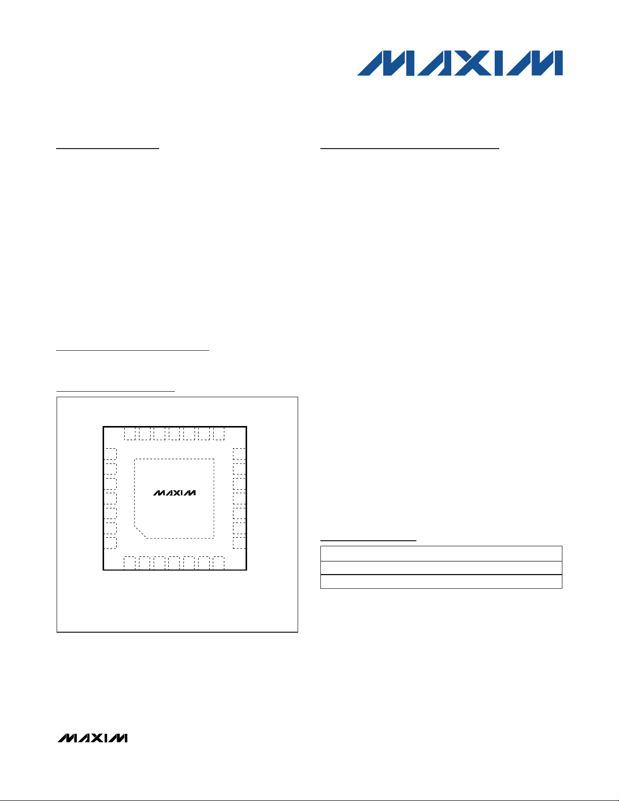
Pin Configuration
Ordering Information
19-4691; Rev 0; 6/09
For pricing, delivery, and ordering information, please contact Maxim Direct at 1-888-629-4642,
or visit Maxim’s website at www.maxim-ic.com.
+
Denotes a lead(Pb)-free/RoHS-compliant package.
T&R = Tape and reel.
*
EP = Exposed pad.
SFP+ Controller with Digital LDD Interface
TOP VIEW
N.C.
V
CC
CSELOUT
SCLOUT
SDAOUT
LOSOUT
OUT1
*EXPOSED PAD.
DAC2
GND
DAC1
2021 19 17 16 15
22
23
24
25
26
27
+
28
12
RSELOUT
(5mm × 5mm × 0.8mm)
DS1874
3
SCL
SDA
THIN QFN
REFIN
GND
18
4567
TXF
LOS
*EP
MON2
IN1
CC
V
TXD
14
MON1
MON3N
13
12
MON3P
MON4
11
10
TXDOUT
RSEL
9
8
GND
PART TEMP RANGE PIN-PACKAGE
DS1874T+ -40°C to +95°C 28 TQFN-EP*
DS1874T+T&R -40°C to +95°C 28 TQFN-EP*
Page 2

DS1874
2 _______________________________________________________________________________________
Absolute Maximum Ratings . . . . . . . . . . . . . . . . . . . . . . . . . . . . . . . . . . . . . . . . . . . . . . . . . . . . . . . . . . . . . . . . . . . . . .5
Recommended Operating Conditions . . . . . . . . . . . . . . . . . . . . . . . . . . . . . . . . . . . . . . . . . . . . . . . . . . . . . . . . . . . . . .5
DC Electrical Characteristics . . . . . . . . . . . . . . . . . . . . . . . . . . . . . . . . . . . . . . . . . . . . . . . . . . . . . . . . . . . . . . . . . . . . .5
DAC1, DAC2 Electrical Characteristics . . . . . . . . . . . . . . . . . . . . . . . . . . . . . . . . . . . . . . . . . . . . . . . . . . . . . . . . . . . . .6
Analog Quick-Trip Characteristics . . . . . . . . . . . . . . . . . . . . . . . . . . . . . . . . . . . . . . . . . . . . . . . . . . . . . . . . . . . . . . . . .6
Analog Voltage Monitoring Characteristics . . . . . . . . . . . . . . . . . . . . . . . . . . . . . . . . . . . . . . . . . . . . . . . . . . . . . . . . . .6
Digital Thermometer Characteristics . . . . . . . . . . . . . . . . . . . . . . . . . . . . . . . . . . . . . . . . . . . . . . . . . . . . . . . . . . . . . . .7
AC Electrical Characteristics . . . . . . . . . . . . . . . . . . . . . . . . . . . . . . . . . . . . . . . . . . . . . . . . . . . . . . . . . . . . . . . . . . . . .7
Timing Characteristics (Control Loop and Quick Trip) . . . . . . . . . . . . . . . . . . . . . . . . . . . . . . . . . . . . . . . . . . . . . . . . .7
3-Wire Digital Interface Specification . . . . . . . . . . . . . . . . . . . . . . . . . . . . . . . . . . . . . . . . . . . . . . . . . . . . . . . . . . . . . . .7
I
2
C AC Electrical Characteristics . . . . . . . . . . . . . . . . . . . . . . . . . . . . . . . . . . . . . . . . . . . . . . . . . . . . . . . . . . . . . . . . . .8
Nonvolatile Memory Characteristics . . . . . . . . . . . . . . . . . . . . . . . . . . . . . . . . . . . . . . . . . . . . . . . . . . . . . . . . . . . . . . .8
Typical Operating Characteristics . . . . . . . . . . . . . . . . . . . . . . . . . . . . . . . . . . . . . . . . . . . . . . . . . . . . . . . . . . . . . . . . .9
Pin Description . . . . . . . . . . . . . . . . . . . . . . . . . . . . . . . . . . . . . . . . . . . . . . . . . . . . . . . . . . . . . . . . . . . . . . . . . . . . . . .10
Block Diagram . . . . . . . . . . . . . . . . . . . . . . . . . . . . . . . . . . . . . . . . . . . . . . . . . . . . . . . . . . . . . . . . . . . . . . . . . . . . . . .11
Typical Operating Circuit . . . . . . . . . . . . . . . . . . . . . . . . . . . . . . . . . . . . . . . . . . . . . . . . . . . . . . . . . . . . . . . . . . . . . . .12
Detailed Description . . . . . . . . . . . . . . . . . . . . . . . . . . . . . . . . . . . . . . . . . . . . . . . . . . . . . . . . . . . . . . . . . . . . . . . . . . .12
MAX3798/MAX3799 DAC Control . . . . . . . . . . . . . . . . . . . . . . . . . . . . . . . . . . . . . . . . . . . . . . . . . . . . . . . . . . . . . .12
BIAS Register/APC Control . . . . . . . . . . . . . . . . . . . . . . . . . . . . . . . . . . . . . . . . . . . . . . . . . . . . . . . . . . . . . . . . . . .12
MODULATION Control . . . . . . . . . . . . . . . . . . . . . . . . . . . . . . . . . . . . . . . . . . . . . . . . . . . . . . . . . . . . . . . . . . . . . .13
BIAS and MODULATION Control During Power-Up . . . . . . . . . . . . . . . . . . . . . . . . . . . . . . . . . . . . . . . . . . . . . . . .14
BIAS and MODULATION Registers as a Function of Transmit Disable (TXD) . . . . . . . . . . . . . . . . . . . . . . . . . . . .15
APC and Quick-Trip Timing . . . . . . . . . . . . . . . . . . . . . . . . . . . . . . . . . . . . . . . . . . . . . . . . . . . . . . . . . . . . . . . . . . .15
Monitors and Fault Detection . . . . . . . . . . . . . . . . . . . . . . . . . . . . . . . . . . . . . . . . . . . . . . . . . . . . . . . . . . . . . . . . .16
Monitors . . . . . . . . . . . . . . . . . . . . . . . . . . . . . . . . . . . . . . . . . . . . . . . . . . . . . . . . . . . . . . . . . . . . . . . . . . . . . .16
Five Quick-Trip Monitors and Alarms . . . . . . . . . . . . . . . . . . . . . . . . . . . . . . . . . . . . . . . . . . . . . . . . . . . . . . . .16
Six ADC Monitors and Alarms . . . . . . . . . . . . . . . . . . . . . . . . . . . . . . . . . . . . . . . . . . . . . . . . . . . . . . . . . . . . .16
ADC Timing . . . . . . . . . . . . . . . . . . . . . . . . . . . . . . . . . . . . . . . . . . . . . . . . . . . . . . . . . . . . . . . . . . . . . . . . . . . .16
Right-Shifting ADC Result . . . . . . . . . . . . . . . . . . . . . . . . . . . . . . . . . . . . . . . . . . . . . . . . . . . . . . . . . . . . . . . . .16
Enhanced RSSI Monitoring (Dual-Range Functionality) . . . . . . . . . . . . . . . . . . . . . . . . . . . . . . . . . . . . . . . . . .17
Low-Voltage Operation . . . . . . . . . . . . . . . . . . . . . . . . . . . . . . . . . . . . . . . . . . . . . . . . . . . . . . . . . . . . . . . . . . . . . .19
Power-On Analog (POA) . . . . . . . . . . . . . . . . . . . . . . . . . . . . . . . . . . . . . . . . . . . . . . . . . . . . . . . . . . . . . . . . . . . .19
Delta-Sigma Outputs (DAC1 and DAC2) . . . . . . . . . . . . . . . . . . . . . . . . . . . . . . . . . . . . . . . . . . . . . . . . . . . . . . . .19
Digital I/O Pins . . . . . . . . . . . . . . . . . . . . . . . . . . . . . . . . . . . . . . . . . . . . . . . . . . . . . . . . . . . . . . . . . . . . . . . . . . . . .21
LOS, LOSOUT . . . . . . . . . . . . . . . . . . . . . . . . . . . . . . . . . . . . . . . . . . . . . . . . . . . . . . . . . . . . . . . . . . . . . . . . . .21
IN1, RSEL, OUT1, RSELOUT . . . . . . . . . . . . . . . . . . . . . . . . . . . . . . . . . . . . . . . . . . . . . . . . . . . . . . . . . . . . . .21
TXF, TXD, TXDOUT . . . . . . . . . . . . . . . . . . . . . . . . . . . . . . . . . . . . . . . . . . . . . . . . . . . . . . . . . . . . . . . . . . . . . .21
TABLE OF CONTENTS
SFP+ Controller with Digital LDD Interface
Page 3

DS1874
_______________________________________________________________________________________ 3
Transmit Fault (TXF) Output . . . . . . . . . . . . . . . . . . . . . . . . . . . . . . . . . . . . . . . . . . . . . . . . . . . . . . . . . . . . . . .22
Die Identification . . . . . . . . . . . . . . . . . . . . . . . . . . . . . . . . . . . . . . . . . . . . . . . . . . . . . . . . . . . . . . . . . . . . . . . . . . .22
3-Wire Master for Controlling the MAX3798/MAX3799 . . . . . . . . . . . . . . . . . . . . . . . . . . . . . . . . . . . . . . . . . . . . . . . .22
Protocol . . . . . . . . . . . . . . . . . . . . . . . . . . . . . . . . . . . . . . . . . . . . . . . . . . . . . . . . . . . . . . . . . . . . . . . . . . . . . . . . . .22
3-Wire Interface Timing . . . . . . . . . . . . . . . . . . . . . . . . . . . . . . . . . . . . . . . . . . . . . . . . . . . . . . . . . . . . . . . . . . . . . . . .23
DS1874 and MAX3798/MAX3799 Communication . . . . . . . . . . . . . . . . . . . . . . . . . . . . . . . . . . . . . . . . . . . . . . . . . . .23
Normal Operation . . . . . . . . . . . . . . . . . . . . . . . . . . . . . . . . . . . . . . . . . . . . . . . . . . . . . . . . . . . . . . . . . . . . . . . . . .23
Manual Operation . . . . . . . . . . . . . . . . . . . . . . . . . . . . . . . . . . . . . . . . . . . . . . . . . . . . . . . . . . . . . . . . . . . . . . . . . .23
Initialization . . . . . . . . . . . . . . . . . . . . . . . . . . . . . . . . . . . . . . . . . . . . . . . . . . . . . . . . . . . . . . . . . . . . . . . . . . . . . . .25
MAX3798/MAX3799 Register Map and DS1874 Corresponding Location . . . . . . . . . . . . . . . . . . . . . . . . . . . . . . .25
I
2
C Communication . . . . . . . . . . . . . . . . . . . . . . . . . . . . . . . . . . . . . . . . . . . . . . . . . . . . . . . . . . . . . . . . . . . . . . . . . . .26
I2C Definitions . . . . . . . . . . . . . . . . . . . . . . . . . . . . . . . . . . . . . . . . . . . . . . . . . . . . . . . . . . . . . . . . . . . . . . . . . . . . .26
I
2
C Protocol . . . . . . . . . . . . . . . . . . . . . . . . . . . . . . . . . . . . . . . . . . . . . . . . . . . . . . . . . . . . . . . . . . . . . . . . . . . . . . .27
Memory Organization . . . . . . . . . . . . . . . . . . . . . . . . . . . . . . . . . . . . . . . . . . . . . . . . . . . . . . . . . . . . . . . . . . . . . . . . . .28
Shadowed EEPROM . . . . . . . . . . . . . . . . . . . . . . . . . . . . . . . . . . . . . . . . . . . . . . . . . . . . . . . . . . . . . . . . . . . . . . . .29
Register Descriptions . . . . . . . . . . . . . . . . . . . . . . . . . . . . . . . . . . . . . . . . . . . . . . . . . . . . . . . . . . . . . . . . . . . . . . . . . .30
Lower Memory Register Map . . . . . . . . . . . . . . . . . . . . . . . . . . . . . . . . . . . . . . . . . . . . . . . . . . . . . . . . . . . . . . . . .30
Table 01h Register Map . . . . . . . . . . . . . . . . . . . . . . . . . . . . . . . . . . . . . . . . . . . . . . . . . . . . . . . . . . . . . . . . . . . . .31
Table 02h Register Map . . . . . . . . . . . . . . . . . . . . . . . . . . . . . . . . . . . . . . . . . . . . . . . . . . . . . . . . . . . . . . . . . . . . .32
Table 04h Register Map . . . . . . . . . . . . . . . . . . . . . . . . . . . . . . . . . . . . . . . . . . . . . . . . . . . . . . . . . . . . . . . . . . . . .33
Table 05h Register Map . . . . . . . . . . . . . . . . . . . . . . . . . . . . . . . . . . . . . . . . . . . . . . . . . . . . . . . . . . . . . . . . . . . . .33
Table 06h Register Map . . . . . . . . . . . . . . . . . . . . . . . . . . . . . . . . . . . . . . . . . . . . . . . . . . . . . . . . . . . . . . . . . . . . .33
Table 07h Register Map . . . . . . . . . . . . . . . . . . . . . . . . . . . . . . . . . . . . . . . . . . . . . . . . . . . . . . . . . . . . . . . . . . . . .34
Table 08h Register Map . . . . . . . . . . . . . . . . . . . . . . . . . . . . . . . . . . . . . . . . . . . . . . . . . . . . . . . . . . . . . . . . . . . . .34
Auxiliary A0h Memory Register Map . . . . . . . . . . . . . . . . . . . . . . . . . . . . . . . . . . . . . . . . . . . . . . . . . . . . . . . . . . . .34
Lower Memory Register Descriptions . . . . . . . . . . . . . . . . . . . . . . . . . . . . . . . . . . . . . . . . . . . . . . . . . . . . . . . . . . .35
Table 01h Register Descriptions . . . . . . . . . . . . . . . . . . . . . . . . . . . . . . . . . . . . . . . . . . . . . . . . . . . . . . . . . . . . . . .48
Table 02h Register Descriptions . . . . . . . . . . . . . . . . . . . . . . . . . . . . . . . . . . . . . . . . . . . . . . . . . . . . . . . . . . . . . . .55
Table 04h Register Description . . . . . . . . . . . . . . . . . . . . . . . . . . . . . . . . . . . . . . . . . . . . . . . . . . . . . . . . . . . . . . . .84
Table 06h Register Descriptions . . . . . . . . . . . . . . . . . . . . . . . . . . . . . . . . . . . . . . . . . . . . . . . . . . . . . . . . . . . . . . .85
Table 07h Register Descriptions . . . . . . . . . . . . . . . . . . . . . . . . . . . . . . . . . . . . . . . . . . . . . . . . . . . . . . . . . . . . . . .86
Table 08h Register Descriptions . . . . . . . . . . . . . . . . . . . . . . . . . . . . . . . . . . . . . . . . . . . . . . . . . . . . . . . . . . . . . . .87
Auxiliary Memory A0h Register Descriptions . . . . . . . . . . . . . . . . . . . . . . . . . . . . . . . . . . . . . . . . . . . . . . . . . . . . .87
Applications Information . . . . . . . . . . . . . . . . . . . . . . . . . . . . . . . . . . . . . . . . . . . . . . . . . . . . . . . . . . . . . . . . . . . . . . .88
Power-Supply Decoupling . . . . . . . . . . . . . . . . . . . . . . . . . . . . . . . . . . . . . . . . . . . . . . . . . . . . . . . . . . . . . . . . . . . .88
SDA and SCL Pullup Resistors . . . . . . . . . . . . . . . . . . . . . . . . . . . . . . . . . . . . . . . . . . . . . . . . . . . . . . . . . . . . . . . .88
Package Information . . . . . . . . . . . . . . . . . . . . . . . . . . . . . . . . . . . . . . . . . . . . . . . . . . . . . . . . . . . . . . . . . . . . . . . . . .88
TABLE OF CONTENTS (continued)
SFP+ Controller with Digital LDD Interface
Page 4

DS1874
SFP+ Controller with Digital LDD Interface
4 _______________________________________________________________________________________
Figure 1. Modulation LUT Loading to MAX3798/MAX3799 MOD DAC . . . . . . . . . . . . . . . . . . . . . . . . . . . . . . . . . . . .13
Figure 2. Power-Up Timing . . . . . . . . . . . . . . . . . . . . . . . . . . . . . . . . . . . . . . . . . . . . . . . . . . . . . . . . . . . . . . . . . . . . .14
Figure 3. TXD Timing . . . . . . . . . . . . . . . . . . . . . . . . . . . . . . . . . . . . . . . . . . . . . . . . . . . . . . . . . . . . . . . . . . . . . . . . . .15
Figure 4. APC Loop and Quick-Trip Sample Timing . . . . . . . . . . . . . . . . . . . . . . . . . . . . . . . . . . . . . . . . . . . . . . . . . .15
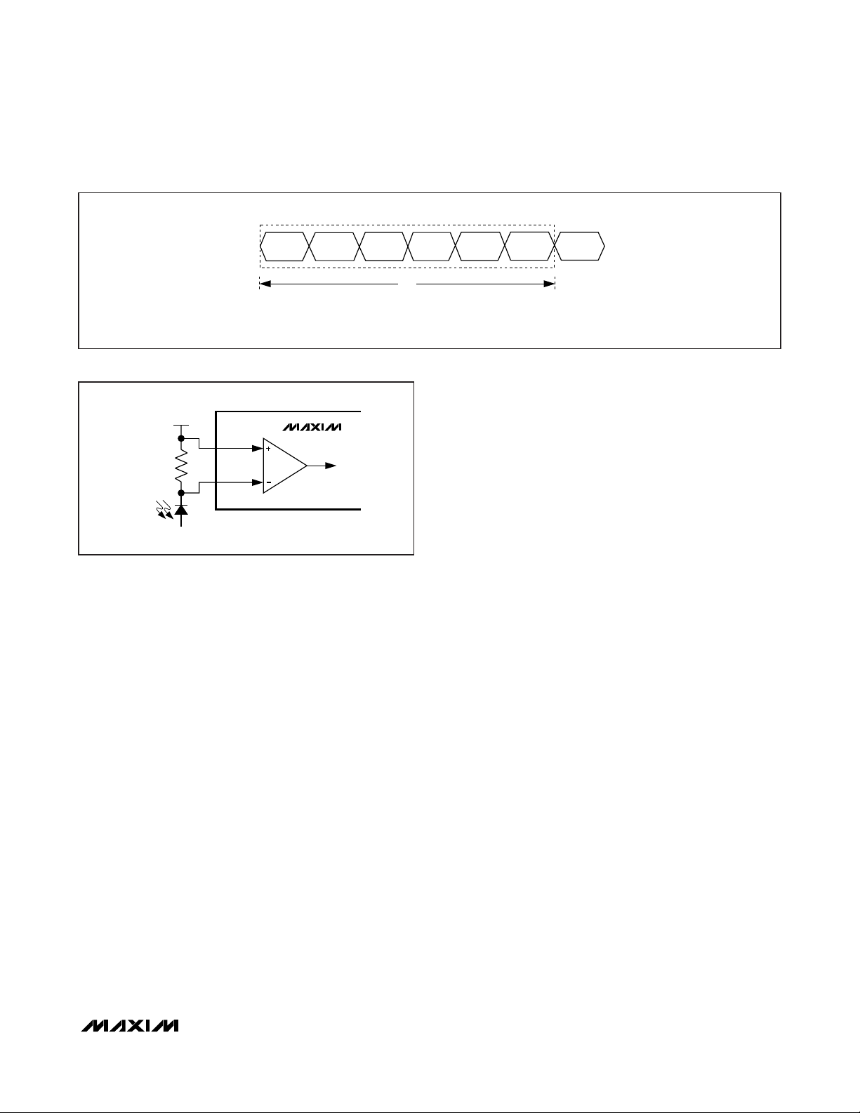
Figure 5. ADC Round-Robin Timing . . . . . . . . . . . . . . . . . . . . . . . . . . . . . . . . . . . . . . . . . . . . . . . . . . . . . . . . . . . . . . .17
Figure 6. MON3 Differential Input for High-Side RSSI . . . . . . . . . . . . . . . . . . . . . . . . . . . . . . . . . . . . . . . . . . . . . . . . .17
Figure 7. RSSI Flowchart . . . . . . . . . . . . . . . . . . . . . . . . . . . . . . . . . . . . . . . . . . . . . . . . . . . . . . . . . . . . . . . . . . . . . . .18
Figure 8. Low-Voltage Hysteresis Example . . . . . . . . . . . . . . . . . . . . . . . . . . . . . . . . . . . . . . . . . . . . . . . . . . . . . . . . .19
Figure 9. Recommended RC Filter for DAC1/DAC2 . . . . . . . . . . . . . . . . . . . . . . . . . . . . . . . . . . . . . . . . . . . . . . . . . .20
Figure 10. Delta-Sigma Outputs . . . . . . . . . . . . . . . . . . . . . . . . . . . . . . . . . . . . . . . . . . . . . . . . . . . . . . . . . . . . . . . . . .20
Figure 11. DAC1/DAC2 LUT Assignments . . . . . . . . . . . . . . . . . . . . . . . . . . . . . . . . . . . . . . . . . . . . . . . . . . . . . . . . . .20
Figure 12. Logic Diagram 1 . . . . . . . . . . . . . . . . . . . . . . . . . . . . . . . . . . . . . . . . . . . . . . . . . . . . . . . . . . . . . . . . . . . . .21
Figure 13. Logic Diagram 2 . . . . . . . . . . . . . . . . . . . . . . . . . . . . . . . . . . . . . . . . . . . . . . . . . . . . . . . . . . . . . . . . . . . . .22
Figure 14a. TXF Nonlatched Operation . . . . . . . . . . . . . . . . . . . . . . . . . . . . . . . . . . . . . . . . . . . . . . . . . . . . . . . . . . . .22
Figure 14b. TXF Latched Operation . . . . . . . . . . . . . . . . . . . . . . . . . . . . . . . . . . . . . . . . . . . . . . . . . . . . . . . . . . . . . . .22
Figure 15. 3-Wire Timing . . . . . . . . . . . . . . . . . . . . . . . . . . . . . . . . . . . . . . . . . . . . . . . . . . . . . . . . . . . . . . . . . . . . . . .23
Figure 16. 3-Wire State Machine . . . . . . . . . . . . . . . . . . . . . . . . . . . . . . . . . . . . . . . . . . . . . . . . . . . . . . . . . . . . . . . . .24
Figure 17. I
2
C Timing . . . . . . . . . . . . . . . . . . . . . . . . . . . . . . . . . . . . . . . . . . . . . . . . . . . . . . . . . . . . . . . . . . . . . . . . . .26
Figure 18. Example I2C Timing . . . . . . . . . . . . . . . . . . . . . . . . . . . . . . . . . . . . . . . . . . . . . . . . . . . . . . . . . . . . . . . . . .28
Figure 19. Memory Map . . . . . . . . . . . . . . . . . . . . . . . . . . . . . . . . . . . . . . . . . . . . . . . . . . . . . . . . . . . . . . . . . . . . . . . .29
Table 1. Acronyms . . . . . . . . . . . . . . . . . . . . . . . . . . . . . . . . . . . . . . . . . . . . . . . . . . . . . . . . . . . . . . . . . . . . . . . . . . . .13
Table 2. Update Rate Timing . . . . . . . . . . . . . . . . . . . . . . . . . . . . . . . . . . . . . . . . . . . . . . . . . . . . . . . . . . . . . . . . . . . .15
Table 3. ADC Default Monitor Full-Scale Ranges . . . . . . . . . . . . . . . . . . . . . . . . . . . . . . . . . . . . . . . . . . . . . . . . . . . .16
Table 4. MON3 Hysteresis Threshold Values . . . . . . . . . . . . . . . . . . . . . . . . . . . . . . . . . . . . . . . . . . . . . . . . . . . . . . .18
Table 5. MON3 Configuration Registers . . . . . . . . . . . . . . . . . . . . . . . . . . . . . . . . . . . . . . . . . . . . . . . . . . . . . . . . . . .18
LIST OF FIGURES
LIST OF TABLES
Page 5
DS1874
Stresses beyond those listed under “Absolute Maximum Ratings” may cause permanent damage to the device. These are stress ratings only, and functional
operation of the device at these or any other conditions beyond those indicated in the operational sections of the specifications is not implied. Exposure to
absolute maximum rating conditions for extended periods may affect device reliability.
Voltage Range on MON1–MON4, RSEL,
IN1, LOS, TXF, and TXD Pins
Relative to Ground .................................-0.5V to (V
CC
+ 0.5V)*
Voltage Range on V
CC
, SDA, SCL, OUT1,
RSELOUT, and LOSOUT Pins
Relative to Ground.................................................-0.5V to +6V
Operating Temperature Range ...........................-40°C to +95°C
Programming Temperature Range .........................0°C to +95°C
Storage Temperature Range .............................-55°C to +125°C
Soldering Temperature...........................Refer to the IPC/JEDEC
J-STD-020 Specification.
DC ELECTRICAL CHARACTERISTICS
(VCC= +2.85V to +3.9V, TA= -40°C to +95°C, unless otherwise noted.)
*
Subject to not exceeding +6V.
RECOMMENDED OPERATING CONDITIONS
(TA= -40°C to +95°C, unless otherwise noted.)
ABSOLUTE MAXIMUM RATINGS
SFP+ Controller with Digital LDD Interface
_______________________________________________________________________________________ 5
Main Supply Voltage VCC (Note 1) +2.85 +3.9 V
High-Level Input Voltage
(SDA, SCL, SDAOUT)
Low-Level Input Voltage
(SDA, SCL, SDAOUT)
High-Level Input Voltage
(TXD, TXF, RSEL, IN1, LOS)
Low-Level Input Voltage
(TXD, TXF, RSEL, IN1, LOS)
PARAMETER SYMBOL CONDITIONS MIN TYP MAX UNITS
V
IH:1
V
-0.3
IL:1
V
2.0
IH:2
V
-0.3 +0.8 V
IL:2
0.7 x
V
CC
VCC+
0.3
0.3 x
V
CC
V
CC
0.3
V
V
+
V
Supply Current ICC (Notes 1, 2) 2.5 10 mA
Output Leakage
(SDA, SDAOUT, OUT1,
RSELOUT, LOSOUT, TXF)
Low-Leve l Output Voltage (SDA,
SDAOUT, SCLOUT, CSELOUT,
OUT1, RSELOUT, LOSOUT,
TXDOUT, DAC1, DAC2, TXF)
High-Level Output Voltage
(DAC1, DAC2, SCLOUT,
SDAOUT, CSELOUT, TXDOUT)
TXDOUT Before EEPROM Reca ll 10 100 nA
DAC1 and DAC2 Before LUT
Recall
Input Leakage Current
(SCL, TXD, LOS, RSEL, IN1)
Digital Power-On Reset POD 1.0 2.2 V
Analog Power-On Reset POA 2.0 2.75 V
PARAMETER SYMBOL CONDITIONS MIN TYP MAX UNITS
I
1 μA
LO
IOL = 4mA 0.4
V
OL
IOL = 6mA 0.6
-
V
V
IOH = 4mA
OH
Figure 11 10 100 nA
I
1 μA
LI
CC
0.4
V
V
Page 6
DS1874
SFP+ Controller with Digital LDD Interface
6 _______________________________________________________________________________________
ANALOG VOLTAGE MONITORING CHARACTERISTICS
(VCC= +2.85V to +3.9V, TA= -40°C to +95°C, unless otherwise noted.)
ANALOG QUICK-TRIP CHARACTERISTICS
(VCC= +2.85V to +3.9V, TA= -40°C to +95°C, unless otherwise noted.)
DAC1, DAC2 ELECTRICAL CHARACTERISTICS
(VCC= +2.85V to +3.9V, TA= -40°C to +95°C, unless otherwise noted.)
Main Oscillator Frequency f
Delta-Sigma Input-Clock
Frequency
Reference Voltage Input (REFIN) V
Output Range 0 V
Output Resolution
Output Impedance RDS 35 100
MON2, TXP HI, TXP LO FullScale Voltage
HBIAS, LOS Full-Scale Voltage 1.25 V
MON2 Input Resistance 35 50 65 k
Resolution 8 Bits
Error TA = +25°C ±2 %FS
Integral Nonlinearity -1 +1 LSB
Differentia l Nonl inearit y -1 +1 LSB
Temperature Drift -2.5 +2.5 %FS
LOS Offset -5 mV
PARAMETER SYMBOL CONDITIONS MIN TYP MAX UNITS
5 MHz
OSC
f
f
DS
Minimum 0.1μF to GND 2 VCC V
REFIN
See the Delta-Sigma Outputs (DAC1 and
DAC2) section for details.
PARAMETER SYMBOL CONDITIONS MIN TYP MAX UNITS
V
2.5 V
APC
9 Bits
/2 MHz
OSC
REFIN
V
ADC Resolution 13 Bit s
Input/Supply Accuracy
(MON1–MON4, V
Update Rate for Temperature,
MON1–MON4, and V
Input/Supply Offset
(MON1–MON4, V
Factor y Setting
PARAMETER SYMBOL CONDITIONS MIN TYP MAX UNITS
)
CC
CC
)
CC
MON1–MON4 2.5
V
CC
MON3 Fine
ACC At factor y setting 0.25 0.50 %FS
tRR 64 75 m s
V
(Note 3) 0 5 LSB
OS
(Note 4)
6.5536
312.5 μV
V
Page 7
DS1874
3-WIRE DIGITAL INTERFACE SPECIFICATION
(VCC= +2.85V to +3.9V, TA= -40°C to +95°C, timing referenced to V
IL(MAX)
and V
IH(MIN)
, unless otherwise noted. See Figure 15.)
SFP+ Controller with Digital LDD Interface
_______________________________________________________________________________________ 7
TIMING CHARACTERISTICS (CONTROL LOOP AND QUICK TRIP)
(VCC= +2.85V to +3.9V, TA= -40°C to +95°C, unless otherwise noted.)
AC ELECTRICAL CHARACTERISTICS
(VCC= +2.85V to +3.9V, TA= -40°C to +95°C, unless otherwise noted.)
DIGITAL THERMOMETER CHARACTERISTICS
(VCC= +2.85V to +3.9V, TA= -40°C to +95°C, unless otherwise noted.)
Thermometer Error T
PARAMETER SYMBOL CONDITIONS MIN TYP MAX UNITS
-40°C to +95°C -3 +3 °C
ERR
TXD Enable t
Recovery from TXD Disable
(Figure 14)
Recovery After Power-Up t
Fault Reset Time (to TXF = 0)
Fault A ss ert Time (to TXF = 1) t
LOSOUT Assert Time t
LOSOUT Deassert Time t
PARAMETER SYMBOL CONDITIONS MIN TYP MAX UNITS
From TXD (Notes 5, 6) 5 μs
OFF
t
From TXD (Notes 5, 7) 1 m s
ON
INIT_DAC
LOSS_ON
LOSS_OFF
From V
t
From TXD 131
INITR1
From V
t
INITR2
FAULT
After HTXP, LTXP, HBATH, IBIASMAX
(Note 9)
LLOS (Notes 9, 10) 6.4 55 μs
HLOS (Notes 9, 11) 6.4 55 μs
> VCC LO alarm (Notes 5, 8) 20 ms
CC
> VCC LO alarm (Note 8) 161
CC
Output-Enable Time Following POA t
Binary Search Time t
PARAMETER SYMBOL CONDITIONS MIN TYP MAX UNITS
(Note 8) 20 ms
INIT
(Note 12) 8 10
SEARCH
ms
6.4 55 μs
BIAS
Samples
SCLOUT Clock Frequency f
SCLOUT Duty Cycle t
SDAOUT Setup Time tDS 100 ns
SDAOUT Hold Time tDH 100 ns
CSELOUT Pulse-Width Low t
CSELOUT Leading Time Before
the First SCLOUT Edge
CSELOUT Trailing Time After the
Last SCLOUT Edge
SDAOUT, SCLOUT Load C
PARAMETER SYMBOL CONDITIONS MIN TYP MAX UNITS
(Note 13) 833 kHz
SCLOUT
50 %
3WDC
500 ns
CSW
t
500 ns
L
t
(Note 14) 500 ns
T
Total bus capacitance on one line (Note 14) 10 pF
B3W
Page 8
Note 1: All voltages are referenced to ground. Current into the IC is positive, and current out of the IC is negative.
Note 2: Inputs are at supply rail. Outputs are not loaded.
Note 3: This parameter is guaranteed by design.
Note 4: Full-scale is user programmable.
Note 5: The DACs are the bias and modulation DACs found in the MAX3798/MAX3799 that are controlled by the DS1874.
Note 6: The DS1874 is configured with TXDOUT connected to the MAX3798/MAX3799 DISABLE input.
Note 7: This includes writing to the modulation DAC and the initial step written to the bias DAC.
Note 8: A temperature conversion is completed and the modulation register value is recalled from the LUT and V
CC
has been
measured to be above V
CC
LO alarm.
Note 9: The timing is determined by the choice of the update rate setting (see Table 02h, Register 88h).
Note 10: This specification is the time it takes from MON3 voltage falling below the LLOS trip threshold to LOSOUT asserted high.
Note 11: This specification is the time it takes from MON3 voltage rising above the HLOS trip threshold to LOSOUT asserted low.
Note 12: Assuming an appropriate initial step is programmed that would cause the power to exceed the APC set point within four
steps, the bias current will be within 3% within the time specified by the binary search time. See the
BIAS and MODULA-
TION Control During Power-Up
section.
Note 13: I
2
C interface timing shown is for fast mode (400kHz). This device is also backward compatible with I2C standard mode
timing.
Note 14: C
B
—the total capacitance of one bus line in pF.
Note 15: EEPROM write begins after a STOP condition occurs.
DS1874
SFP+ Controller with Digital LDD Interface
8 _______________________________________________________________________________________
NONVOLATILE MEMORY CHARACTERISTICS
(VCC= +2.85V to +3.9V, unless otherwise noted.)
I2C AC ELECTRICAL CHARACTERISTICS
(VCC= +2.85V to +3.9V, TA= -40°C to +95°C, timing referenced to V
IL(MAX)
and V
IH(MIN)
, unless otherwise noted. See Figure 17.)
SCL Clock Frequency f
Cloc k Pulse-Width Low t
Cloc k Pulse-Width High t
Bus-Free Time Between STOP and START
Condition
START Hold Time t
START Setup Time t
Data Out Hold T ime t
Data In Setup Time t
Rise Time of Both SDA and SCL Signals tR (Note 14) 20 + 0.1CB 300 ns
Fal l Time of Both SDA and SCL Signals tF (Note 14) 20 + 0.1CB 300 ns
STOP Setup Time t
EEPROM Write Time tW (Note 15) 20 ms
Capacitive Load for Each Bus Line CB 400 pF
PARAMETER SYMBOL CONDITIONS MIN TYP MAX UNITS
(Note 13) 0 400 kHz
SCL
1.3 μs
LOW
0.6 μs
HIGH
t
1.3 μs
BUF
0.6 μs
HD: STA
0.6 μs
SU:STA
0 0.9 μs
HD:DAT
100 ns
SU:DAT
0.6 μs
SU:STO
EEPROM Write Cycles
PARAMETER SYMBOL CONDITIONS MIN TYP MAX UNITS
At +25°C 200,000
At +85°C 50,000
Page 9
DS1874
SFP+ Controller with Digital LDD Interface
_______________________________________________________________________________________
9
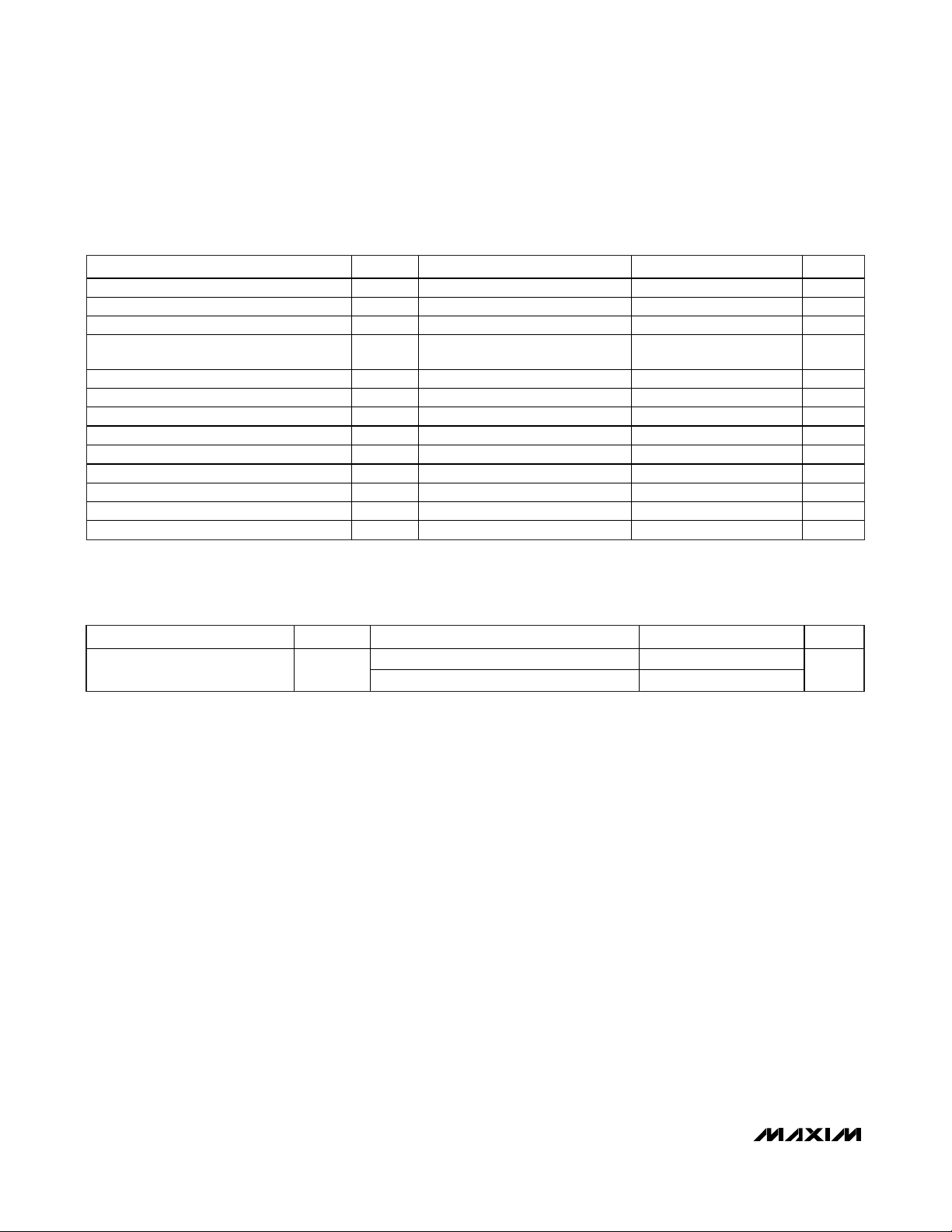
Typical Operating Characteristics
(VCC= +2.85V to +3.9V, TA= +25°C, unless otherwise noted.)
SUPPLY CURRENT vs. SUPPLY VOLTAGE
SDA = SCL = V
2.9
2.7
2.5
2.3
2.1
SUPPLY CURRENT (mA)
1.9
1.7
1.5
2.85
CC
+25°C
+95°C
-40°C
VCC (V)
DS1874 toc01
3.853.603.10 3.35
SUPPLY CURRENT vs. TEMPERATURE
2.7
SDA = SCL = V
2.6
2.5
2.4
2.3
SUPPLY CURRENT (mA)
2.2
2.1
2.0
-40
MON1–MON4 DNL
1.0
USING FACTORY-PROGRAMMED
0.8
FULL-SCALE VALUE OF 2.5V
0.6
0.4
0.2
0
-0.2
-0.4
MON1–MON4 DNL (LSB)
-0.6
-0.8
-1.0
0 2.5
MON1–MON4 INPUT VOLTAGE (V)
2.01.51.00.5
1.0
0.8
DS1874 toc04
0.6
0.4
0.2
0
-0.2
-0.4
DAC1 AND DAC2 DNL (LSB)
-0.6
-0.8
-1.0
0
DAC1 AND DAC2 POSITION (DEC)
CC
VCC = 3.9V
VCC = 2.85V
VCC = 3.3V
TEMPERATURE (°C)
DAC1 AND DAC2 DNL
MON1–MON4 INL
1.0
USING FACTORY-PROGRAMMED
0.8
DS1874 toc02
806040200-20
DS1874 toc05
500400300200100
FULL-SCALE VALUE OF 2.5V
0.6
0.4
0.2
0
-0.2
-0.4
MON1–MON4 INL (LSB)
-0.6
-0.8
-1.0
0 2.5
MON1–MON4 INPUT VOLTAGE (V)
DAC1 AND DAC2 INL
2.0
1.5
1.0
0.5
0
-0.5
DAC1 AND DAC2 INL (LSB)
-1.0
-1.5
-2.0
0
DAC1 AND DAC2 POSITION (DEC)
DS1874 toc03
2.01.51.00.5
DS1874 toc06
500400100 200 300
Page 10

DS1874
SFP+ Controller with Digital LDD Interface
10 ______________________________________________________________________________________
Pin Description
PIN NAME FUNCTION
1 RSELOUT Rate-Select Output
2 SCL I2C Serial-Clock Input
3 SDA I2C Serial-Data Input/Output
4 TXF Transmit-Fault Input and Output. The output is open drain.
5 LOS Loss-of-Signal Input
6 IN1 Digital Input. General-purpose input with AS1 in SFF-8079 or RS1 in SFF-8431.
7 TXD Transm it-Disab le Input
8, 17, 21 GND Ground Connection
9 RSEL Rate-Select Input
10 TXDOUT Transmit-Disable Output
11 MON4 External Monitor Input 4
12, 13
14 MON1 External Monitor Input 1 and HBATH Quick Trip
15, 23 VCC Power-Supply Input
16 MON2 External Monitor Input 2. Feedback vo ltage for APC loop and HTXP/LTXP quick trip.
18 REFIN Reference Input for DAC1 and DAC2
19, 20 DAC1, DAC2 Delta-Sigma Output 1/2
22 N.C. No Connect ion
24 CSELOUT
25 SCLOUT
26 SDAOUT
27 LOSOUT Open-Drain Receive Loss-of-Signal Output
28 OUT1 Digital Output. General-purpose output with AS1 output in SFF-8079 or RS1 output in SFF-8431.
— EP Exposed Pad
MON3P,
MON3N
Differentia l External Monitor Input 3 and LOS Quick Trip
Chip-Select Output. Part of the 3-wire interface to the MAX3798/MAX3799 laser driver/l imiting
amplifier.
Serial-Clock Output. Part of the 3-wire interface to the MAX3798/MAX3799 laser driver/limiting
amplifier.
Serial-Data Input/Output. Part of the 3-wire interface to the MAX3798/MAX3799 laser driver/limiting
amplifier.
Page 11
DS1874
SFP+ Controller with Digital LDD Interface
______________________________________________________________________________________ 11
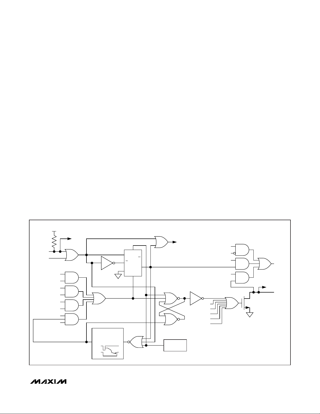
Block Diagram
V
SDA
SCL
V
MON1
MON2
MON3P
MON3N
MON4
V
CC
CC
I2C
INTERFACE
EEPROM
256 BYTES
AT A0h
CC
ANALOG MUX
TEMPERATURE
SENSOR
MAIN MEMORY
EEPROM/SRAM
ADC CONFIGURATION/RESULTS,
SYSTEM STATUS/CONTROL BITS,
ALARMS/WARNINGS,
LOOKUP TABLES,
USER MEMORY
13-BIT
ADC
INTEGRATOR
8-BIT
QTs
POWER-ON
ANALOG
INTERRUPT
APC
9-BIT
DELTA-SIGMA
9-BIT
DELTA-SIGMA
3-WIRE
INTERFACE
V
CC
REFIN
DAC1
DAC2
SDAOUT
SCLOUT
CSELOUT
TXF
TXD
RSEL
IN1
LOS
SEE
FIGURE 13
SEE
FIGURE 12
DS1874
TXDOUT
RSELOUT
OUT1
LOSOUT
GND
Page 12
DS1874
SFP+ Controller with Digital LDD Interface
12 ______________________________________________________________________________________
Detailed Description
The DS1874 integrates the control and monitoring functionality required to implement a VCSEL-based SFP or
SFP+ system using Maxim’s MAX3798/MAX3799 combined limiting amplifier and laser driver. Key components of the DS1874 are shown in the
Block Diagram
and described in subsequent sections.
MAX3798/MAX3799 DAC Control
The DS1874 controls two 9-bit DACs inside the
MAX3798/MAX3799. One DAC is used for laser bias
control while the other is used for laser modulation control. The DS1874 communicates with the MAX3798/
MAX3799 over a 3-wire digital interface (see the
3-Wire
Master for Controlling the MAX3798/MAX3799
section).
The communication between the DS1874 and
MAX3798/MAX3799 is transparent to the end user.
BIAS Register/APC Control
The MAX3798/MAX3799 control their laser bias current
DAC using the APC loop within the DS1874. The APC
loop’s feedback to the DS1874 is the monitor diode
(MON2) current, which is converted to a voltage using
Typical Operating Circuit
+3.3V
100Ω
PIN-ROSA
3W
VCSEL-TOSA
BMON
LA
LDD
MAX3798/MAX3799
MODE
DAC
BIAS
DAC
DISABLE
LOS
RSEL
FAULT
3W
MON1
MON2
MON3
R
BD
R
MON
DS1874
EEPROM
QUICK
TRIP
ADC
LOS
TXF
TXD
TXDOUT
SDA
I2C
SCL
RSEL
RSELOUT
LOS
LOSOUT
TX_FAULT
TX_DISABLE
MODE_DEF2 (SDA)
MODE_DEF1 (SCL)
RATE SELECT
LOS
Page 13
an external resistor. The feedback is sampled by a comparator and compared to a digital set-point value. The
output of the comparator has three states: up, down, or
no-operation. The no-operation state prevents the output
from excessive toggling once steady state is reached.
As long as the comparator output is in either the up or
down states, the bias is adjusted by writing increment
and decrement values to the MAX3798/MAX3799
through the BIASINC register (3-wire address 13h).
The DS1874 has an LUT to allow the APC set point to
change as a function of temperature to compensate for
tracking error (TE). The TE LUT has 36 entries that
determine the APC setting in 4°C windows between
-40°C to +100°C.
MODULATION Control
The MAX3798/MAX3799 control the laser modulation
using the internal temperature-indexed LUT within the
DS1874. The modulation LUT is programmed in 2°C
increments over the -40°C to +102°C range to provide
temperature compensation for the laser’s modulation.
The modulation is updated after each temperature conversion using the 3-wire interface that connects to the
MAX3798/MAX3799. The MAX3798/MAX3799 include a
9-bit DAC. The modulation LUT is 8 bits.
Figure 1 demonstrates how the 8-bit LUT controls the
9-bit DAC with the use of a temperature control bit
(MODTC, Table 02h, Register C6h) and a temperature
index register (MODTI, Table 02h, Register C2h).
DS1874
______________________________________________________________________________________ 13
Table 1. Acronyms
SFP+ Controller with Digital LDD Interface
Figure 1. Modulation LUT Loading to MAX3798/MAX3799 MOD DAC
ACRONYM DEFINITION
ADC Analog-to-Digital Converter
AGC Automatic Gain Control
APC Automatic Power Control
APD Avalanche Photodiode
ATB Alarm Trap Bytes
BM Burst Mode
DAC Digital-to-Analog Converter
LOS Loss of Signal
LUT Lookup Table
NV Nonvolatile
QT Quic k Trip
TE Track ing Error
TIA Transimpedance Amplif ier
ROSA Receiver Optical Subassembly
SEE Shadowed EEPROM
SFF Small Form Factor
SFF-8472
SFP Small Form Factor Pluggable
SFP+ Enhanced SFP
TOSA Transmit Optical Subassembly
TXP Transm it Power
Document Defining Register Map of SFPs
and SFFs
MODTI
8
7
6
5
4
3
MAX3798/MAX3799 DAC BIT
2
1
0
MODTC = 0
MOD LUT
LOADED TO [8:1]
MOD LUT
LOADED TO [7:0]
-40 +102
TEMPERATURE (°C)
(DAC BIT 0 = 0)
MODTI
8
7
6
5
4
3
MAX3798/MAX3799 DAC BIT
2
1
0
-40 +102
MOD LUT
LOADED TO [8:1]
(DAC BIT 0 = 0)
TEMPERATURE (°C)
MODTC = 1
MOD LUT
LOADED TO [7:0]
Page 14
DS1874
SFP+ Controller with Digital LDD Interface
14 ______________________________________________________________________________________
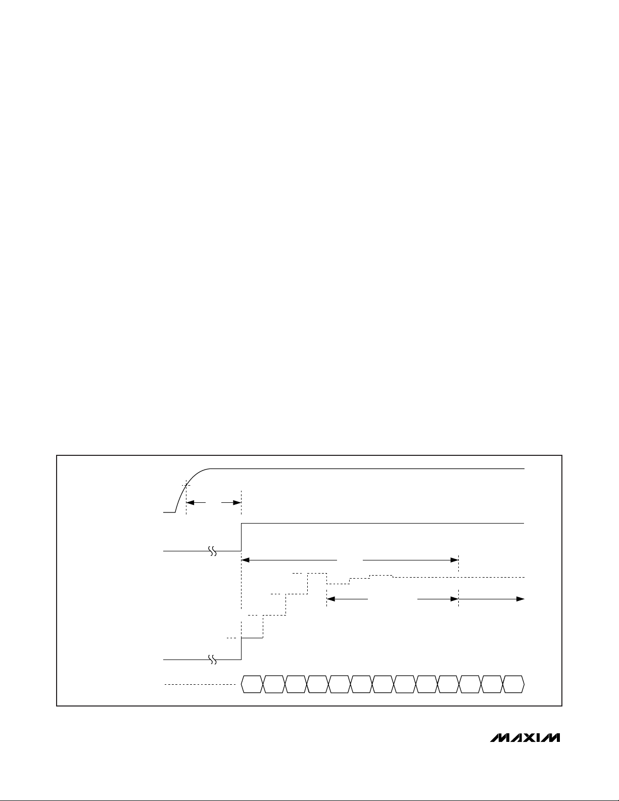
BIAS and MODULATION Control
During Power-Up
The DS1874 has two internal registers, MODULATION
and BIAS, that represent the values written to the
MAX3798/MAX3799’s modulation DAC and bias DAC
through the 3-wire interface. On power-up, the DS1874
sets the MODULATION and BIAS registers to 0. When
VCCis above POA, the DS1874 initializes the MAX3798/
MAX3799. After a temperature conversion is completed
and if the VCC LO alarm is enabled, an additional V
CC
conversion above the customer-defined VCC LO alarm
level is required before the MAX3798/MAX3799 MODULATION register is updated with the value determined
by the temperature conversion and the modulation LUT.
When the MODULATION register is set, the BIAS register is set to a value equal to ISTEP (see Figure 2). The
startup algorithm checks if this bias current causes a
feedback voltage above the APC set point, and if not, it
continues increasing the BIAS register by ISTEP until the
APC set point is exceeded. When the APC set point is
exceeded, the device begins a binary search to quickly
reach the bias current corresponding to the proper
power level. After the binary search is completed, the
APC integrator is enabled and single LSB steps are
used to tightly control the average power.
The TXP HI, TXP LO, HBAL, and BIAS MAX QT alarms
are masked until the binary search is completed.
However, the BIAS MAX alarm is monitored during this
time to prevent the BIAS register from exceeding
IBIASMAX. During the bias current initialization, the
BIAS register is not allowed to exceed IBIASMAX. If this
occurs during the ISTEP sequence, then the binary
search routine is enabled. If IBIASMAX is exceeded
during the binary search, the next smaller step is activated. ISTEP or binary increments that would cause the
BIAS register to exceed IBIASMAX are not taken.
Masking the alarms until the completion of the binary
search prevents false positive alarms during startup.
ISTEP is programmed by the customer using Table
02h, Register BBh. During the first steps, the MAX3798/
MAX3799’s bias DAC is directly written using
SET_IBIAS (3-wire address 09h). ISTEP should be programmed to the maximum safe increase that is allowable during startup. If this value is programmed too
low, the DS1874 still operates, but it could take significantly longer for the algorithm to converge and hence
to control the average power.
If a fault is detected, and TXD is toggled to reenable
the outputs, the DS1874 powers up following a similar
sequence to an initial power-up. The only difference is
that the DS1874 already has determined the present
temperature, so the t
INIT
time is not required for the
DS1874 to recall the APC and MOD set points from
EEPROM.
Figure 2. Power-Up Timing
V
V
CC
MODULATION REGISTER
BIAS REGISTER
BIAS SAMPLE
POA
t
INIT
ISTEP
t
SEARCH
4x ISTEP
3x ISTEP
2x ISTEP
12345678910111213
BINARY SEARCH
APC INTEGRATOR ON
Page 15
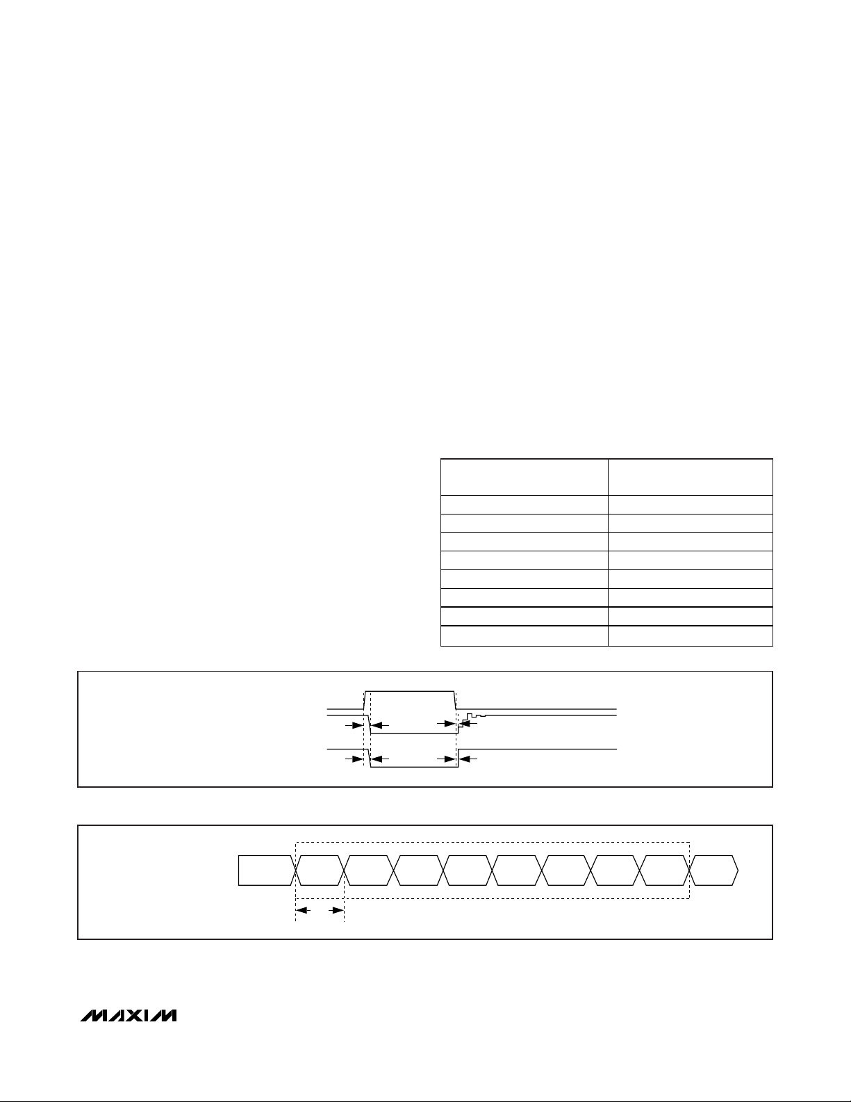
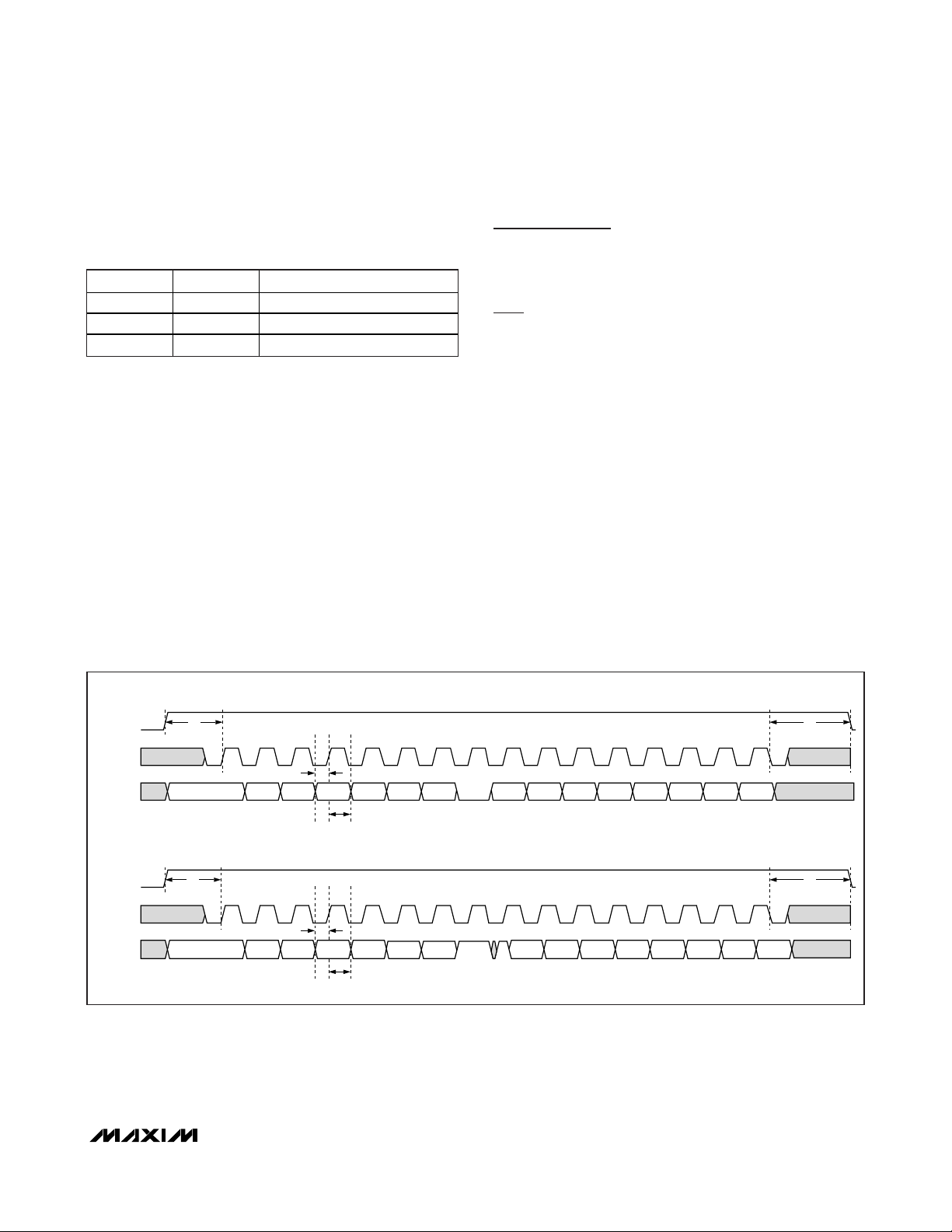
BIAS and MODULATION Registers as a
Function of Transmit Disable (TXD)
If TXD is asserted (logic 1) during normal operation, the
outputs are disabled within t
OFF
. When TXD is deasserted (logic 0), the DS1874 sets the MODULATION register with the value associated with the present
temperature, and initializes the BIAS register using the
same search algorithm as done at startup. When
asserted, soft TXD (TXDC) (Lower Memory, Register
6Eh) would allow a software control identical to the TXD
pin (see Figure 3).
APC and Quick-Trip Timing
As shown in Figure 4, the DS1874’s input comparator is
shared between the APC control loop and the quicktrip alarms (TXP HI, TXP LO, LOS, and BIAS HI). The
comparator polls the alarms in a multiplexed sequence.
Five of every eight comparator readings are used for
APC loop bias-current control. The other three updates
are used to check the HTXP/LTXP (monitor diode voltage), the HBATH (MON1), and LOS (MON3) signals
against the internal APC, BIAS, and MON3 reference,
respectively. If the last APC comparison was higher
than the APC set point, it makes an HTXP comparison,
and if it is lower, it makes an LTXP comparison.
Depending on the results of the comparison, the corresponding alarms and warnings (TXP HI, TXP LO) are
asserted or deasserted.
The DS1874 has a programmable comparator sample
time based on an internally generated clock to facilitate
a wide variety of external filtering options and time
delays resulting from writing values to the MAX3798/
MAX3799’s bias DAC. The UPDATE RATE register
(Table 02h, Register 88h) determines the sampling
time. Samples occur at a regular interval, t
REP
. Table 2
shows the sample rate options available. Any quick-trip
alarm that is detected by default remains active until a
subsequent comparator sample shows the condition no
longer exists. A second bias current monitor (BIAS
MAX) compares the MAX3798/MAX3799’s BIAS DAC’s
code to a digital value stored in the IBIASMAX register.
This comparison is made at every bias current update
to ensure that a high-bias current is quickly detected.
An APC sample that requires an update of the BIAS
register causes subsequent APC samples to be
DS1874
SFP+ Controller with Digital LDD Interface
______________________________________________________________________________________ 15
Figure 4. APC Loop and Quick-Trip Sample Timing
Table 2. Update Rate Timing
Figure 3. TXD Timing
APC_SR[2:0]
000b 800
001b 1200
010b 1600
011b 2000
100b 2800
101b 3200
110b 4400
111b 6400
SAMPLE PERIOD (t
(ns)
REP
)
TXD
BIAS REGISTER
MODULATION REGISTER
APC QUICK-TRIP SAMPLE TIMES
HBIAS
SAMPLE
APC
SAMPLE
t
REP
APC
SAMPLE
t
OFF
t
OFF
APC
SAMPLE
APC
SAMPLE
t
ON
t
ON
APC
SAMPLE
HTXP/LTXP
SAMPLE
LOS
SAMPLE
HBIAS
SAMPLE
APC
SAMPLE
Page 16
DS1874
SFP+ Controller with Digital LDD Interface
16 ______________________________________________________________________________________
ignored until the end of the 3-wire communication that
updates the MAX3798/MAX3799’s BIAS DAC, plus an
additional 16 sample periods (t
REP
).
Monitors and Fault Detection
Monitors
Monitoring functions on the DS1874 include five quick-trip
comparators and six ADC channels. This monitoring
combined with the alarm enables (Table 01h/05h) determines when/if the DS1874 turns off the MAX3798/
MAX3799 DACs and triggers the TXF and TXDOUT outputs. All the monitoring levels and interrupt masks are
user programmable.
Five Quick-Trip Monitors and Alarms
Five quick-trip monitors are provided to detect potential
laser safety issues and LOS status. These monitor the
following:
1) High Bias Current (HBATH)
2) Low Transmit Power (LTXP)
3) High Transmit Power (HTXP)
4) Max Output Current (IBIASMAX)
5) Loss-of-Signal (LOS LO)
The high-transmit and low-transmit power quick-trip registers (HTXP and LTXP) set the thresholds used to compare against the MON2 voltage to determine if the
transmit power is within specification. The HBATH quick
trip compares the MON1 input (generally from the
MAX3798/MAX3799 bias monitor output) against its
threshold setting to determine if the present bias current
is above specification. The BIAS MAX quick trip determines if the BIAS register is above specification. The
BIAS register is not allowed to exceed the value set in
the IBIASMAX register. When the DS1874 detects that
the bias is at the limit it sets the BIAS MAX status bit
and holds the BIAS register setting at the IBIASMAX
level. The bias and power quick trips are routed to the
TXF through interrupt masks to allow combinations of
these alarms to be used to trigger these outputs. The
user can program up to eight different temperatureindexed threshold levels for MON1 (Table 02h,
Registers D0h–D7h). The LOS LO quick trip compares
the MON3 input against its threshold setting to determine if the present received power is below the specification. The LOS LO quick trip can be used to set the
LOSOUT pin. These alarms can be latched using Table
02h, Register 8Ah.
Six ADC Monitors and Alarms
The ADC monitors six channels that measure temperature (internal temp sensor), VCC, and MON1–MON4
using an analog multiplexer to measure them round
robin with a single ADC (see the
ADC Timing
section).
The five voltage channels have a customer-programmable full-scale range and all channels have a customerprogrammable offset value that is factory programmed to
default value (see Table 3). Additionally, MON1–MON4
can right-shift results by up to 7 bits before the results
are compared to alarm thresholds or read over the I2C
bus. This allows customers with specified ADC ranges to
calibrate the ADC full scale to a factor of 1/2nof their
specified range to measure small signals. The DS1874
can then right-shift the results by n bits to maintain the bit
weight of their specification (see the
Right-Shifting ADC
Result
and
Enhanced RSSI Monitoring (Dual-Range
Functionality)
sections).
The ADC results (after right-shifting, if used) are compared to the alarm and warning thresholds after each
conversion, and the corresponding alarms are set,
which can be used to trigger the TXF output. These
ADC thresholds are user programmable, as are the
masking registers that can be used to prevent the
alarms from triggering the TXF output.
ADC Timing
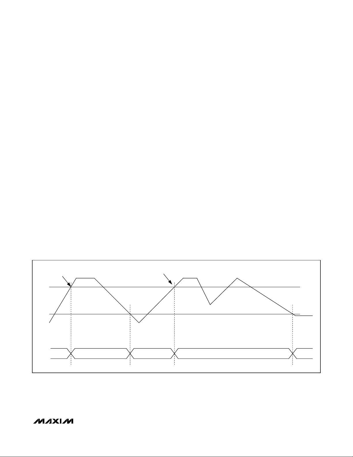
There are six analog channels that are digitized in a
round-robin fashion in the order shown in Figure 5. The
total time required to convert all six channels is tRR(see
the
Electrical Characteristics
for details).
Right-Shifting ADC Result
If the weighting of the ADC digital reading must conform to a predetermined full-scale (PFS) value defined
by a standard’s specification (e.g., SFF-8472), then
right-shifting can be used to adjust the PFS analog
measurement range while maintaining the weighting of
the ADC results. The DS1874’s range is wide enough to
cover all requirements; when the maximum input value
is ≤ 1/2 of the FS value, right-shifting can be used to
obtain greater accuracy. For instance, the maximum
voltage might be 1/8 the specified PFS value, so only
1/8 the converter’s range is effective over this range.
An alternative is to calibrate the ADC’s full-scale range
to 1/8 the readable PFS value and use a right-shift
value of 3. With this implementation, the resolution of
Table 3. ADC Default Monitor Full-Scale
Ranges
SIGNAL
Temperature (°C) 127.996 7FFF -128 8000
VCC (V) 6.5528 FFF8 0 0000
MON1–MON4 (V) 2.4997 FFF8 0 0000
+FS
SIGNAL
+FS
hex
-FS
SIGNAL
-FS
hex
Page 17
DS1874
SFP+ Controller with Digital LDD Interface
______________________________________________________________________________________ 17
the measurement is increased by a factor of 8, and
because the result is digitally divided by 8 by rightshifting, the bit weight of the measurement still meets
the standard’s specification (i.e., SFF-8472).
The right-shift operation on the ADC result is carried out
based on the contents of right-shift control registers (Table
02h, Registers 8Eh–8Fh) in EEPROM. Four analog channels, MON1–MON4, each have 3 bits allocated to set the
number of right-shifts. Up to seven right-shift operations
are allowed and are executed as a part of every conversion before the results are compared to the high-alarm
and low-alarm levels, or loaded into their corresponding
measurement registers (Lower Memory, Registers
64h–6Bh). This is true during the setup of internal calibration as well as during subsequent data conversions.
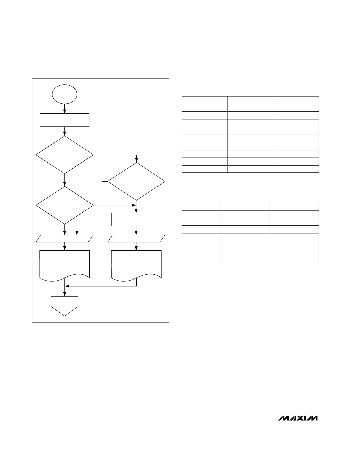
Enhanced RSSI Monitoring (Dual-Range
Functionality)
The DS1874 offers a feature to improve the accuracy
and range of MON3, which is most commonly used for
monitoring RSSI. The accuracy of the RSSI measurements is increased at the small cost of reduced range
(of input signal swing). The DS1874 eliminates this
trade-off by offering “dual range” calibration on the
MON3 channel (see Figure 6). This feature enables
right-shifting (along with its gain and offset settings)
when the input signal is below a set threshold (within the
range that benefits using right-shifting) and then automatically disables right-shifting (recalling different gain and
offset settings) when the input signal exceeds the threshold. Also, to prevent “chattering,” hysteresis prevents
excessive switching between modes in addition to ensuring that continuity is maintained. Dual-range operation is
enabled by default (factory programmed in EEPROM).
However, it can easily be disabled through the RSSI_FC
and RSSI_FF bits, which are described in the
Register
Descriptions
section. When dual-range operation is disabled, MON3 operates identically to the other MON
channels, although featuring a differential input.
Dual-range functionality consists of two modes of operation: fine mode and coarse mode. Each mode is calibrated for a unique transfer function, hence the term, dual
range. Table 5 highlights the registers related to MON3.
Fine mode is equivalent to the other MON channels. Fine
mode is calibrated using the gain, offset, and right-shifting registers at locations shown in Table 5 and is ideal
for relatively small analog input voltages. Coarse mode is
automatically switched to when the input exceeds a
threshold (to be discussed in a subsequent paragraph).
Coarse mode is calibrated using different gain and offset
registers, but lacks right-shifting (since coarse mode is
only used on large input signals). The gain and offset
registers for coarse mode are also shown in Table 5.
Additional information for each of the registers can be
found in the
Register Descriptions
section.
Dual-range operation is transparent to the end user.
The results of MON3 analog-to-digital conversions are
still stored/reported in the same memory locations
(68h–69h, Lower Memory) regardless of whether the
conversion was performed in fine mode or coarse
mode. The only way to tell which mode generated the
digital result is by reading the RSSIS bit.
When the DS1874 is powered up, analog-to-digital conversions begin in a round-robin fashion. Every MON3
timeslice begins with a fine mode analog-to-digital conversion (using fine mode’s gain, offset, and right-shifting
settings). See the flowchart in Figure 7 for more details.
Figure 6. MON3 Differential Input for High-Side RSSI
Figure 5. ADC Round-Robin Timing
ONE ROUND-ROBIN ADC CYCLE
TEMP V
NOTE: IF THE VCC LO ALARM IS ENABLED AT POWER-UP, THE ADC ROUND-ROBIN TIMING CYCLES BETWEEN TEMPERATURE AND VCC ONLY UNTIL VCC
IS ABOVE THE V
100Ω
ROSA
ALARM LOW THRESHOLD.
CC
V
CC
MON3P
MON3N
DS1874
MON1 MON2 MON3 MON4 TEMP
CC
ADC
t
RR
Page 18
DS1874
SFP+ Controller with Digital LDD Interface
18 ______________________________________________________________________________________
Then, depending on whether the last MON3 timeslice
resulted in a coarse-mode conversion and also depending on the value of the current fine conversion, decisions
are made whether to use the current fine-mode conversion result or to make an additional conversion (within
the same MON3 timeslice), using coarse mode (using
coarse mode’s gain and offset settings and no rightshifting) and reporting the coarse-mode result. The flowchart in Figure 7 also illustrates how hysteresis is
implemented. The fine-mode conversion is compared to
one of two thresholds. The actual threshold values are a
function of the number of right-shifts being used. With
the use of right-shifting, the fine mode full-scale is programmed to (1/2
N
th) of the coarse mode full-scale. The
DS1874 now auto ranges to choose the range that gives
the best resolution for the measurement. Hysteresis is
applied to eliminate chatter when the input resides at
the boundary of the two ranges. See Figure 7 for details.
Table 4 shows the threshold values for each possible
number of right-shifts.
The RSSI_FF and RSSI_FC bits are used to force finemode or coarse-mode conversions, or to disable the
dual-range functionality. Dual-range functionality is
enabled by default (both RSSI_FC and RSSI_FF are
factory programmed to 0 in EEPROM). It can be disabled by setting RSSI_FC to 0 and RSSI_FF to 1. These
bits are also useful when calibrating MON3. For additional information, see Figure 19.
Table 5. MON3 Configuration Registers
Figure 7. RSSI Flowchart
Table 4. MON3 Hysteresis Threshold
Values
*
This is the minimum reported coarse-mode conversion.
MON3
TIMESLICE
PERFORM FINE-
MODE CONVERSION
DID PRIOR MON3
TIMESLICE RESULT IN A
COARSE CONVERSION?
(LAST RSSI = 1?)
DID CURRENT FINE-
MODE CONVERSION
REACH MAX?
LAST RSSI = 0
REPORT FINE
CONVERSION RESULT
NUMBER OF
RIGHT-SHIFTS
0 FFF8 F000
1 7FFC 7800
2 3FFE 3C00
3 1FFF 1E00
Y
N
Y
N
N
WAS CURRENT FINE-
MODE CONVERSION
≥ 93.75% OF FS?
Y
PERFORM COARSEMODE CONVERSION
LAST RSSI = 1
REPORT COARSE
CONVERSION RESULT
RIGHT-SHIFT
MON3 VALUE 68h–69h, Lower Memory
4 0FFF 0F00
5 07FF 0780
6 03FF 03C0
7 01FF 01E0
REGISTER FINE MODE COARSE MODE
GAIN 98h–99h, Table 02h 9Ch–9Dh, Table 04h
OFFSET A8h–A9h, Table 02h ADh–ACh, Table 04h
0
CNFGC 8Bh, Table 02h
CONFIG
(RSSIS BIT)
FINE MODE
MAX (hex)
8Fh, Table 04h —
77h, Lower Memory
COARSE MODE
MIN* (hex)
END OF MON3
TIMESLICE
Page 19
DS1874
Low-Voltage Operation
The DS1874 contains two power-on reset (POR) levels.
The lower level is a digital POR (POD) and the higher
level is an analog POR (POA). At startup, before the
supply voltage rises above POA, the outputs are disabled, all SRAM locations are set to their defaults,
shadowed EEPROM (SEE) locations are zero, and all
analog circuitry is disabled. When VCCreaches POA,
the SEE is recalled, and the analog circuitry is enabled.
While V
CC
remains above POA, the device is in its normal operating state, and it responds based on its nonvolatile configuration. If during operation V
CC
falls
below POA, but is still above POD, then the SRAM
retains the SEE settings from the first SEE recall, but the
device analog is shut down and the outputs disabled. If
the supply voltage recovers back above POA, then the
device immediately resumes normal operation. If the
supply voltage falls below POD, then the device SRAM
is placed in its default state and another SEE recall is
required to reload the nonvolatile settings. The EEPROM
recall occurs the next time V
CC
exceeds POA. Figure 8
shows the sequence of events as the voltage varies.
Any time VCCis above POD, the I2C interface can be
used to determine if VCCis below the POA level. This is
accomplished by checking the RDYB bit in the STATUS
(Lower Memory, Register 6Eh) byte. RDYB is set when
VCCis below POA; when VCCrises above POA, RDYB
is timed (within 500µs) to go to 0, at which point the
part is fully functional.
For all device addresses sourced from EEPROM (Table
02h, Register 8Ch), the default device address is A2h
until V
CC
exceeds POA, allowing the device address to
be recalled from the EEPROM.
Power-On Analog (POA)
POA holds the DS1874 in reset until VCCis at a suitable
level (V
CC
> POA) for the device to accurately measure
with its ADC and compare analog signals with its quicktrip monitors. Because VCCcannot be measured by the
ADC when VCCis less than POA, POA also asserts the
VCC LO alarm, which is cleared by a VCCADC conversion greater than the customer-programmable V
CC
alarm low ADC limit. This allows a programmable limit
to ensure that the headroom requirements of the transceiver are satisfied during a slow power-up. The TXF
output does not latch until there is a conversion above
VCClow limit. The POA alarm is nonmaskable. The TXF
output is asserted when VCCis below POA. See the
Low-Voltage Operation
section for more information.
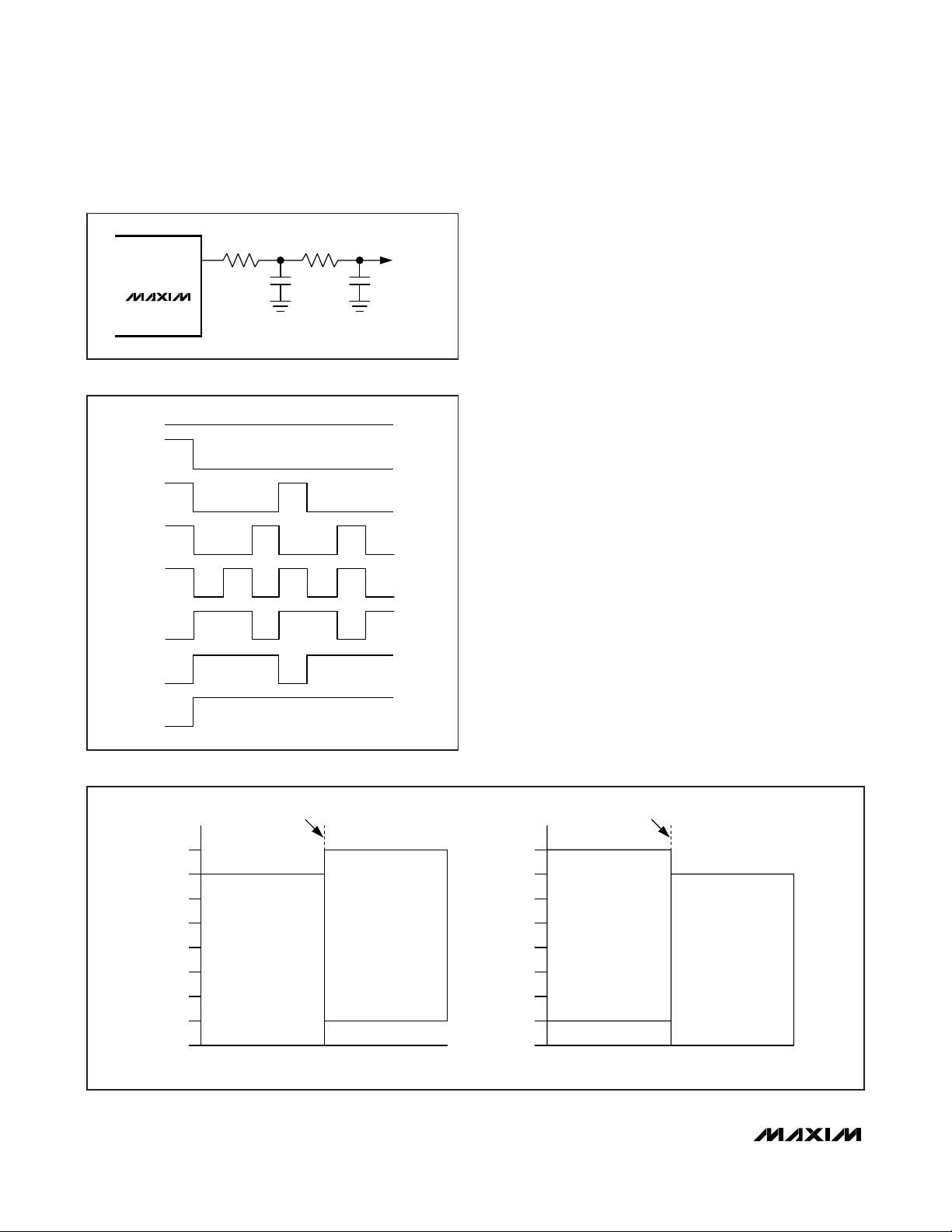
Delta-Sigma Outputs (DAC1 and DAC2)
Two delta-sigma outputs are provided, DAC1 and
DAC2. With the addition of an external RC filter, these
outputs provide two 9-bit resolution analog outputs with
the full-scale range set by the input REFIN. Each output
SFP+ Controller with Digital LDD Interface
______________________________________________________________________________________ 19
Figure 8. Low-Voltage Hysteresis Example
SEE RECALL
V
POA
V
CC
V
POD
PRECHARGED
SEE RECALLED VALUE RECALLED VALUE
TO 0
SEE RECALL
PRECHARGED TO 0
PRECHARGED
TO 0
Page 20
DS1874
is either manually controlled or controlled using a temperature-indexed LUT. A delta-sigma is a digital output
using pulse-density modulation. It provides much lower
output ripple than a standard digital PWM output given
the same clock rate and filter components. Before t
INIT
,
the DAC1 and DAC2 outputs are high impedance.
The external RC filter components are chosen based
on ripple requirements, output load, delta-sigma frequency, and desired response time. A recommended
filter is shown in Figure 9.
The DS1874’s delta-sigma outputs are 9 bits. For illustrative purposes, a 3-bit example is provided. Each
possible output of this 3-bit delta-sigma DAC is given in
Figure 10.
In LUT mode, DAC1 and DAC2 are each controlled by a
separate 8-bit, 4°C-resolution, temperature-addressed
LUT. The delta-sigma outputs use a 9-bit structure. The
8-bit LUTs are either loaded directly into the MSBs (8:1)
or the LSBs (7:0). This is determined by DAC1TI (Table
02h, Register C3h), DAC2TI (Table 02h, Register C4h),
DAC1TC (Table 02h, Register C6h, bit 6), and DAC2TC
(Table 02h, Register C6h, bit 5). See Figure 11 for more
details. The DAC1 LUT (Table 07h) and DAC2 LUT
(Table 08h) are nonvolatile and password-2 protected.
The reference input, REFIN, is the supply voltage for
the output buffer of DAC1 and DAC2. The voltage connected to REFIN must be able to support the edge rate
requirements of the delta-sigma outputs. In a typical
application, a 0.1µF capacitor should be connected
between REFIN and ground.
20 ______________________________________________________________________________________
Figure 11. DAC1/DAC2 LUT Assignments
SFP+ Controller with Digital LDD Interface
Figure 10. Delta-Sigma Outputs
Figure 9. Recommended RC Filter for DAC1/DAC2
DAC1/DAC2
3.24kΩ 3.24kΩ
0.01μF 0.01μF
DS1874
0
1
2
3
4
5
6
7
OUTPUT
DAC[1/2]TI
8
7
6
5
4
3
DELTA-SIGMA DACA OR DACB
2
1
0
DAC[1/2]TC = 0
LUT LOADED TO [8:1]
(DAC BIT 0 = 0)
LUT LOADED TO [7:0]
-40 +102
TEMPERATURE (°C)
8
7
6
5
LUT LOADED TO [8:1]
4
3
DELTA-SIGMA DACA OR DACB
2
1
0
(DAC BIT 0 = 0)
-40 +102
DAC[1/2]TI
DAC[1/2]TC = 1
LUT LOADED TO [7:0]
TEMPERATURE (°C)
Page 21
DS1874
SFP+ Controller with Digital LDD Interface
______________________________________________________________________________________ 21
Digital I/O Pins
Five digital input and five digital output pins are provided for monitoring and control.
LOS, LOSOUT
By default (LOSC = 1, Table 02h, Register 89h), the
LOS pin is used to convert a standard comparator output for loss of signal (LOS) to an open-collector output.
This means the mux shown in the
Block Diagram
by
default selects the LOS pin as the source for the
LOSOUT output transistor. The output of the mux can
be read in the STATUS byte (Table 01h, Register 6Eh)
as the RXL bit. The RXL signal can be inverted (INV
LOS = 1) before driving the open-drain output transistor
using the XOR gate provided. Setting LOSC = 0 configures the mux to be controlled by LOS LO, which is driven by the output of the LOS quick trip (Table 02h,
Registers BEh and BFh). The mux setting (stored in
EEPROM) does not take effect until V
CC
> POA, allow-
ing the EEPROM to recall.
IN1, RSEL, OUT1, RSELOUT
The digital input IN1 and RSEL pins primarily serve to
meet the rate-select requirements of SFP and SFP+.
They also serve as general-purpose inputs. OUT1 and
RSELOUT are driven by a combination of the IN1,
RSEL, and logic dictated by control registers in the
EEPROM (Figure 13). The levels of IN1 and RSEL can
be read using the STATUS register (Lower Memory,
Register 6Eh). The open-drain output OUT1 can be
controlled and/or inverted using the CNFGB register
(Table 02h, Register 8Ah). The open-drain RSELOUT
output is software-controlled and/or inverted through
the Status register and CNFGA register (Table 02h,
Register 89h). External pullup resistors must be provided on OUT1 and RSELOUT to realize high logic levels.
TXF, TXD, TXDOUT
TXDOUT is generated from a combination of TXF, TXD,
and the internal signal FETG. A software control identical to TXD is available (TXDC, Lower Memory, Register
6Eh). A TXD pulse is internally extended (TXD
EXT
) by
time t
INITR1
to inhibit the latching of low alarms and
warnings related to the APC loop to allow for the loop to
stabilize. The nonlatching alarms and warnings are TXP
LO, LOS LO, and MON1–MON4 LO alarms and warnings. In addition, TXP LO is disabled from creating
FETG. TXF is both an input and an output (Figure 12).
See the
Transmit Fault (TXF) Output
section for a
detailed explanation of TXF. Figure 12 shows that the
Figure 12. Logic Diagram 1
V
CC
R
PU
TXD
TXDC
TXP HI FLAG
TXP HI ENABLE
BIAS MAX
BIAS MAX ENABLE
HBAL FLAG
HBAL ENABLE
TXP LO FLAG
TXP LO ENABLE
TXDS
TXD
EXT
FAULT RESET TIMER
(130ms)
OUT IN
IN
OUT
SET BIAS REGISTER TO 0 AND
MAX3798/MAX3799
SET_IMOD TO 0
R
C
Q
C
Q
D
S
POWER-ON
FETG
MINT
HBAL FLAG
TXP LO FLAG
TXP LO FLAG
BIAS MAX FLAG
RESET
TXD
TXDIO
TXDFG
TXDFLT
TXDOUT
TXF
TXF
Page 22
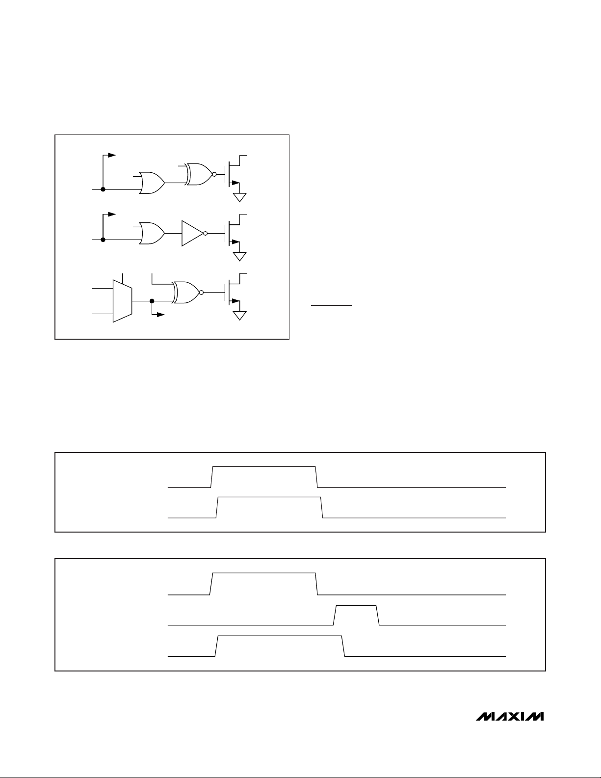
DS1874
same signals and faults can also be used to generate
the internal signal FETG (Table 01h/05h, Registers FAh
and FBh). FETG is used to send a fast “turn-off” command to the laser driver. The intended use is a direct
connection to the MAX3798/MAX3799’s TXD input if
this is desired. When V
CC
< POA, TXDOUT is high
impedance.
Transmit Fault (TXF) Output
TXF can be triggered by all alarms, warnings, and
quick trips (Figure 12). The six ADC alarms, warnings,
and the LOS quick trips require enabling (Table
01h/05h, Registers F8h and FDh). See Figures 14a and
14b for nonlatched and latched operation. Latching of
the alarms is controlled by the CNFGB and CNFGC
registers (Table 02h, Registers 8Ah–8Bh).
Die Identification
The DS1874 has an ID hardcoded in its die. Two registers (Table 02h, Registers CEh–CFh) are assigned for
this feature. The CEh register reads 74h to identify the
part as the DS1874, while the CFh register reads the
current device version.
3-Wire Master for Controlling
the MAX3798/MAX3799
The DS1874 controls the MAX3798/MAX3799 over a
proprietary 3-wire interface. The DS1874 acts as the
master, initiating communication with and generating
the clock for the MAX3798/MAX3799. It is a 3-pin interface consisting of SDAOUT (a bidirectional data line),
an SCLOUT clock signal, and a CSELOUT chip-select
output (active high).
Protocol
The DS1874 initiates a data transfer by asserting the
CSELOUT pin. It then starts to generate a clock signal
22 ______________________________________________________________________________________
Figure 14b. TXF Latched Operation
SFP+ Controller with Digital LDD Interface
Figure 14a. TXF Nonlatched Operation
Figure 13. Logic Diagram 2
IN1S OUT1
INVOUT1
IN1C
IN1
RSEL
LOS
LOS LO
RSELS
RSELC
INV LOSLOSC
MUX
RXL
RSELOUT
LOSOUT
DETECTION OF TXF FAULT
TXF
DETECTION OF TXF FAULT
TXD
TXF
Page 23
after the CSELOUT has been set to 1. Each operation
consists of 16-bit transfers (15-bit address/data, 1-bit
RWN). All data transfers are MSB first.
Write Mode (RWN = 0): The master generates 16 clock
cycles at SCLOUT in total. It outputs 16 bits (MSB first)
to the SDAOUT line at the falling edge of the clock. The
master closes the transmission by setting the
CSELOUT to 0.
Read Mode (RWN = 1): The master generates 16 clock
cycles at SCLOUT in total. It outputs 8 bits (MSB first)
to the SDAOUT line at the falling edge of the clock. The
SDAOUT line is released after the RWN bit has been
transmitted. The slave outputs 8 bits of data (MSB first)
at the rising edge of the clock. The master samples
SDAOUT at the falling edge of SCLOUT. The master
closes the transmission by setting the CSELOUT to 0.
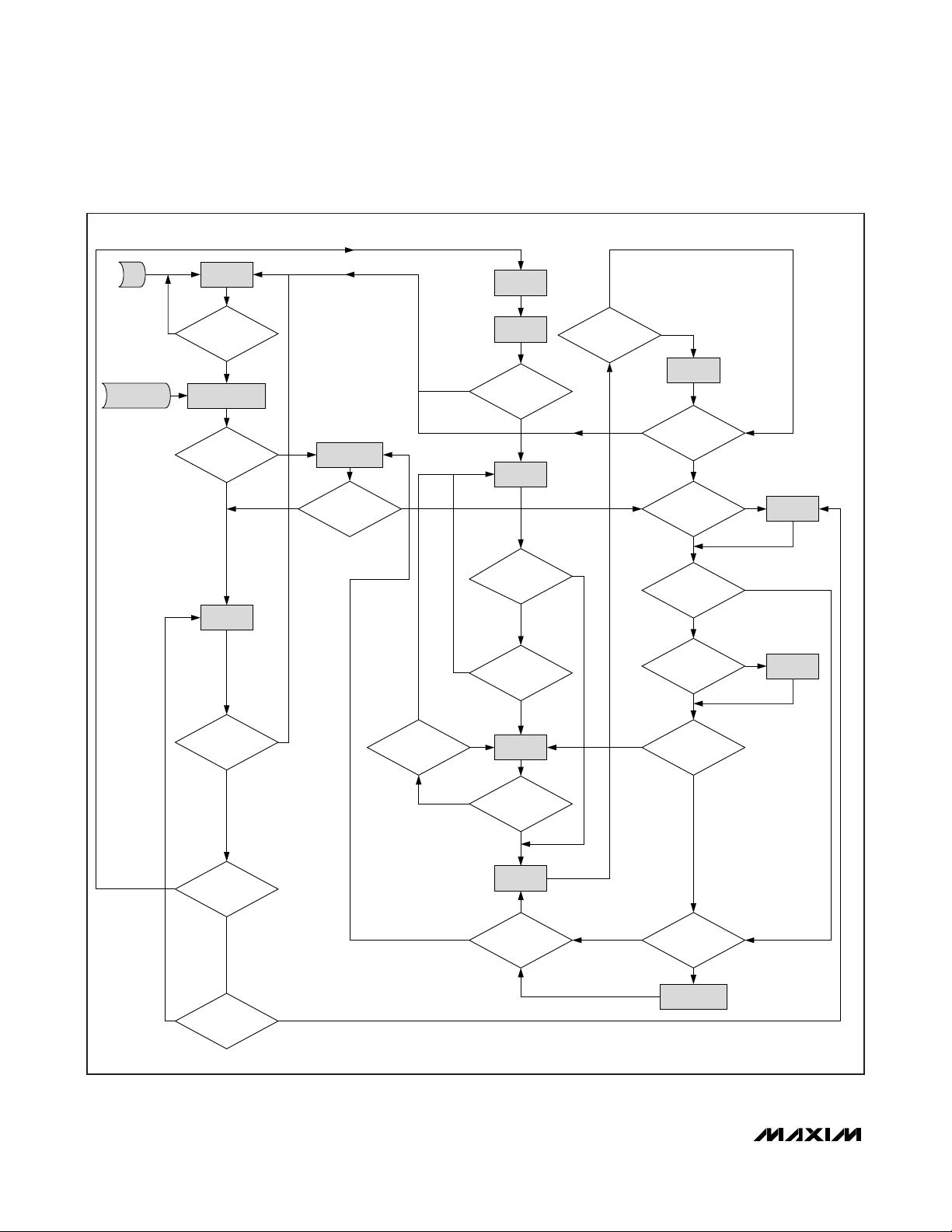
3-Wire Interface Timing
Figure 15 shows the 3-wire interface timing. Figure 16
shows the 3-wire state machine. See the
3-Wire Digital
Interface Specification
table for more information.
DS1874 and MAX3798/MAX3799
Communication
Normal Operation
The majority of the communication between the two
devices consists of bias adjustments for the APC loop.
After each temperature conversion, the laser modulation setting must be updated. Status registers TXSTAT1
and TXSTAT2 are read between temperature updates
at a regular interval: tRR(see the
Electrical Characteristics
table). The results are stored in TXSTAT1 and TXSTAT2
(Table 02h, F4h–F5h).
Manual Operation
The MAX3798/MAX3799 are manually controllable
using four registers in the DS1874: 3WCTRL,
ADDRESS, WRITE, and READ. Commands can be
manually issued while the DS1874 is in normal operation mode. It is also possible to suspend normal 3-wire
commands so that only manual operation commands
are sent (3WCTRL, Table 02h, Register F8h).
DS1874
SFP+ Controller with Digital LDD Interface
______________________________________________________________________________________ 23
Figure 15. 3-Wire Timing
BIT NAME DESCRIPTION
15:9 Address 7-bit internal register address
8 RWN 0: write; 1: read
7:0 Data 8-bit read or write data
WRITE MODE
CSELOUT
SCLOUT
SDAOUT
READ MODE
CSELOUT
SCLOUT
SDAOUT
t
L
t
L
A6 A5 A4 A3 A2 A1 A0
12345678A69 1011121314150
t
DS
A5 A4 A3 A2 A1 RWN D7 D6 D5 D4 D3 D2 D1 D0
t
DH
1234567891011121314150
t
DS
t
DH
A0
D7 D6 D5 D4 D3 D2 D1 D0RWN
t
T
t
T
Page 24
DS1874
24 ______________________________________________________________________________________
Figure 16. 3-Wire State Machine
SFP+ Controller with Digital LDD Interface
RESET FLAGS HERE
POR
YES
SET TXD FLAG HERE
TXD_LATCHED = 1
SET RTXPOR2_FLAG HERE
READ TXPOR1
TX_POR = 1?
NO
WRITE MOD, BIAS = 00
UPDATE CTRL
TXD = = 0?
YES
READ TXPOR2
UPDATE
MODULATION
YES
NO
TXD HIGH_STDBY
1011
YES
TXD = = 0?
NO
NO
READ TXPOR3
TX_POR = = 1?
START APC
LOOP
APC_BINARY = = 1?
YES
BIASINC = = 1?
YES
TXDIS = 1?
STROBE
NO
NO
READ TXPOR4
TX_POR = = 1?
NO
MAN_MODE_RDWR = 1?
TXD_FLAG = = 1
OR TXDIS = 1 OR
RTXPOR2 FLAG
NO
MODINC = = 1?
NO
YES
YES
READ/WRITE
MANMODE
INCREMENT
MODULATION
NO
TX_POR = = 1?
NO
MODINC = 1?
MAN_MODE_RDWR = 1?
YES
BIASINC = = 1?
YES YES
UPDATE BIAS
APC_BINARY = = 1?
NO
STANDBY
NO
TXD_FLAG = = 1? OR
RTXPOR2 FLAG = 1
NO
BIASINC = = 1?
NO
TEMP_CONV_START = = 1?
AND TXDIS = 0
UPDATE
TXSTAT, BIAS, MOD
YES YES
Page 25
Initialization
During initialization, the DS1874 transfers all its 3-wire
EEPROM control registers to the MAX3798/MAX3799.
The 3-wire control registers include the following:
• RXCTRL1
• RXCTRL2
• SET_CML
• SET_LOS
• TXCTRL
• IMODMAX
• IBIASMAX
• SET_PWCTRL
• SET_TXDE
The control registers are first written when V
CC
exceeds
POA. They are also written if the MAX3798/MAX3799
TX_POR bit is set high (visible in 3W TXSTAT1, bit 7). In
the MAX3798/MAX3799, this bit is “sticky” (latches high
and is cleared on a read). They are also updated on a
rising edge of TXD. Any time one of these events
occurs, the DS1874 reads and updates TXSTAT1 and
TXSTAT2 and sets SET_IBIAS and SET_IMOD in the
MAX3798/MAX3799 to 0.
DS1874
SFP+ Controller with Digital LDD Interface
______________________________________________________________________________________ 25
MAX3798/MAX3799 Register Map and DS1874 Corresponding Location
Note: This register is not present in the DS1874. To access this register, use manual operation (see the
Manual Operation
section).
MAX3798/MAX3799 REGISTER FUNCTION REGISTER NAME DS1874 LOCATION
Receiver Control 1 RXCTRL1 Table 02h, E8h
Receiver Control 2 RXCTRL2 Table 02h, E9h
Receiver Status RXSTAT Lower Memory, 6Eh, Bit1
Output CML Level Setting SET_CML Table 02h, EAh
LOS Threshold Level Setting SET_LOS Table 02h, EBh
Transm itter Control TXCTRL Table 02h, ECh
Transm itter Status 1 TXSTAT1 Table 02h, FCh
Transm itter Status 2 TXSTAT2 Table 02h, FDh
Bias Current Setting SET_IBIAS/BIAS Table 02h, CBh –CCh
Modulation Current Setting SET_IMOD/MODULATION Table 02h, 8Ah–8Bh
Maximum Modulation Current Setting IMODMAX Table 02h, EDh
Max imum Bias Current Setting IBIASMAX Table 02h, EEh
Modulation Current Increment Setting MODINC (see Note)
Automatical ly performed by APC loop. Disable
Bias Current Increment Setting BIASINC
Mode Control MODECTRL (see Note)
Transm itter Pulse-Width Control SET_PWCTRL Table 02h, EFh
Transm itter Deemphasis Control SET_TXDE Table 02h, F0h
APC before using 3-wire manual mode. Manual
Mode: Table 02h, F8h–FAh
Page 26
DS1874
SFP+ Controller with Digital LDD Interface
26 ______________________________________________________________________________________
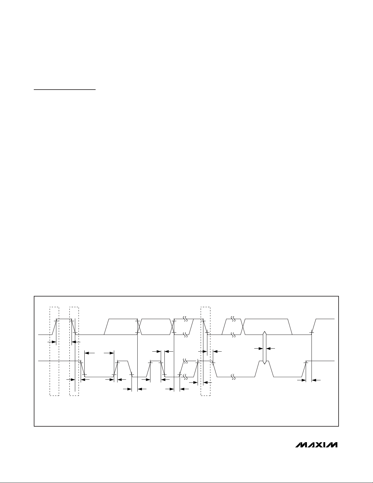
Figure 17. I2C Timing
I2C Communication
I2C Definitions
The following terminology is commonly used to
describe I2C data transfers.
Master device: The master device controls the
slave devices on the bus. The master device generates SCL clock pulses and START and STOP
conditions.
Slave devices: Slave devices send and receive
data at the master’s request.
Bus idle or not busy: Time between STOP and
START conditions when both SDA and SCL are inactive and in their logic-high states.
START condition: A START condition is generated
by the master to initiate a new data transfer with a
slave. Transitioning SDA from high to low while SCL
remains high generates a START condition. See
Figure 17 for applicable timing.
STOP condition: A STOP condition is generated by
the master to end a data transfer with a slave.
Transitioning SDA from low to high while SCL
remains high generates a STOP condition. See
Figure 17 for applicable timing.
Repeated START condition: The master can use a
repeated START condition at the end of one data
transfer to indicate that it will immediately initiate a
new data transfer following the current one.
Repeated STARTs are commonly used during read
operations to identify a specific memory address to
begin a data transfer. A repeated START condition
is issued identically to a normal START condition.
See Figure 17 for applicable timing.
Bit write: Transitions of SDA must occur during the
low state of SCL. The data on SDA must remain valid
and unchanged during the entire high pulse of SCL
plus the setup and hold time requirements (Figure
17). Data is shifted into the device during the rising
edge of the SCL.
Bit read: At the end a write operation, the master
must release the SDA bus line for the proper amount
of setup time (Figure 17) before the next rising edge
of SCL during a bit read. The device shifts out each
bit of data on SDA at the falling edge of the previous
SCL pulse and the data bit is valid at the rising edge
of the current SCL pulse. Remember that the master
generates all SCL clock pulses, including when it is
reading bits from the slave.
Acknowledgement (ACK and NACK): An acknowledgement (ACK) or not acknowledge (NACK) is
always the ninth bit transmitted during a byte transfer. The device receiving data (the master during a
read or the slave during a write operation) performs
an ACK by transmitting a zero during the ninth bit. A
device performs a NACK by transmitting a one during the 9th bit. Timing (Figure 17) for the ACK and
NACK is identical to all other bit writes. An ACK is
the acknowledgment that the device is properly
receiving data. A NACK is used to terminate a read
SDA
t
BUF
t
LOW
SCL
t
HD:STA
STOP START REPEATED
NOTE: TIMING IS REFERENCED TO V
IL(MAX)
AND V
IH(MIN)
t
R
t
HD:DAT
.
t
HIGH
t
F
t
SU:DAT
START
t
SU:STA
t
HD:STA
t
SP
t
SU:STO
Page 27

sequence or as an indication that the device is not
receiving data.
Byte write: A byte write consists of 8 bits of information transferred from the master to the slave (most
significant bit first) plus a 1-bit acknowledgement
from the slave to the master. The 8 bits transmitted
by the master are done according to the bit-write
definition and the acknowledgement is read using
the bit-read definition.
Byte read: A byte read is an 8-bit information transfer from the slave to the master plus a 1-bit ACK or
NACK from the master to the slave. The 8 bits of
information that are transferred (most significant bit
first) from the slave to the master are read by the
master using the bit-read definition, and the master
transmits an ACK using the bit-write definition to
receive additional data bytes. The master must
NACK the last byte read to terminate communication
so the slave returns control of SDA to the master.
Slave address byte: Each slave on the I2C bus
responds to a slave address byte sent immediately
following a START condition. The slave address byte
contains the slave address in the most significant 7
bits and the R/W bit in the least significant bit.
The DS1874 responds to two slave addresses. The
auxiliary memory always responds to a fixed I2C
slave address, A0h. The Lower Memory and Tables
00h–08h respond to I2C slave addresses that can
be configured to any value between 00h–FEh using
the DEVICE ADDRESS byte (Table 02h, Register
8Ch). The user also must set the ASEL bit (Table
02h, Register 89h) for this address to be active. By
writing the correct slave address with R/W = 0, the
master indicates it will write data to the slave. If R/W
= 1, the master reads data from the slave. If an
incorrect slave address is written, the DS1874
assumes the master is communicating with another
I2C device and ignores the communications until the
next START condition is sent. If the main device’s
slave address is programmed to be A0h, access to
the auxiliary memory is disabled.
Memory address: During an I2C write operation to
the DS1874, the master must transmit a memory
address to identify the memory location where the
slave is to store the data. The memory address is
always the second byte transmitted during a write
operation following the slave address byte.
I2C Protocol
Writing a single byte to a slave: The master must
generate a START condition, write the slave address
byte (R/W = 0), write the memory address, write the
byte of data, and generate a STOP condition.
Remember the master must read the slave’s
acknowledgement during all byte-write operations.
Writing multiple bytes to a slave: To write multiple
bytes to a slave, the master generates a START condition, writes the slave address byte (R/W = 0),
writes the memory address, writes up to 8 data
bytes, and generates a STOP condition. The
DS1874 writes 1 to 8 bytes (one page or row) with a
single write transaction. This is internally controlled
by an address counter that allows data to be written
to consecutive addresses without transmitting a
memory address before each data byte is sent. The
address counter limits the write to one 8-byte page
(one row of the memory map). Attempts to write to
additional pages of memory without sending a STOP
condition between pages results in the address
counter wrapping around to the beginning of the
present row.
For example, a 3-byte write starts at address 06h
and writes 3 data bytes (11h, 22h, and 33h) to three
“consecutive” addresses. The result is that addresses 06h and 07h would contain 11h and 22h, respectively, and the third data byte, 33h, would be written
to address 00h.
To prevent address wrapping from occurring, the
master must send a STOP condition at the end of
the page, then wait for the bus-free or EEPROM
write time to elapse. Then the master can generate a
new START condition and write the slave address
byte (R/W = 0) and the first memory address of the
next memory row before continuing to write data.
Acknowledge polling: Any time a EEPROM page is
written, the DS1874 requires the EEPROM write time
(t
W
) after the STOP condition to write the contents of
the page to EEPROM. During the EEPROM write
time, the DS1874 will not acknowledge its slave
address because it is busy. It is possible to take
advantage of that phenomenon by repeatedly
addressing the DS1874, which allows the next page
to be written as soon as the DS1874 is ready to
receive the data. The alternative to acknowledge
polling is to wait for maximum period of tWto elapse
before attempting to write again to the DS1874.
EEPROM write cycles: When EEPROM writes occur,
the DS1874 writes the whole EEPROM memory page,
even if only a single byte on the page was modified.
Writes that do not modify all 8 bytes on the page are
allowed and do not corrupt the remaining bytes of
memory on the same page. Because the whole page
is written, bytes on the page that were not modified
during the transaction are still subject to a write
DS1874
______________________________________________________________________________________ 27
SFP+ Controller with Digital LDD Interface
Page 28

DS1874
SFP+ Controller with Digital LDD Interface
28 ______________________________________________________________________________________
Figure 18. Example I2C Timing
cycle. This can result in a whole page being worn out
over time by writing a single byte repeatedly. Writing
a page one byte at a time wears the EEPROM out
eight times faster than writing the entire page at
once. The DS1874’s EEPROM write cycles are specified in the
Nonvolatile Memory Characteristics
table.
The specification shown is at the worst-case temperature. It can handle approximately ten times that
many writes at room temperature. Writing to SRAMshadowed EEPROM memory with SEEB = 1 does not
count as an EEPROM write cycle when evaluating
the EEPROM’s estimated lifetime.
Reading a single byte from a slave: Unlike the
write operation that uses the memory address byte
to define where the data is to be written, the read
operation occurs at the present value of the memory
address counter. To read a single byte from the
slave, the master generates a START condition,
writes the slave address byte with R/W = 1, reads
the data byte with a NACK to indicate the end of the
transfer, and generates a STOP condition.
Manipulating the address counter for reads: A
dummy write cycle can be used to force the address
pointer to a particular value. To do this, the master
generates a START condition, writes the slave
address byte (R/W = 0), writes the memory address
where it desires to read, generates a repeated
START condition, writes the slave address byte (R/W
= 1), reads data with ACK or NACK as applicable,
and generates a STOP condition.
Memory Organization
The DS1874 features nine separate memory tables that
are internally organized into 8-byte rows.
The Lower Memory is addressed from 00h to 7Fh and
contains alarm and warning thresholds, flags, masks,
several control registers, password entry area (PWE),
and the table-select byte.
Table 01h primarily contains user EEPROM (with PW1
level access) as well as alarm and warning-enable
bytes.
Table 02h is a multifunction space that contains configuration registers, scaling and offset values, passwords,
interrupt registers as well as other miscellaneous control bytes.
Table 04h contains a temperature-indexed LUT for
control of the modulation voltage. The modulation LUT
can be programmed in 2°C increments over the -40°C
to +102°C range.
2
TYPICAL I
C WRITE TRANSACTION
MSB LSB
START
1 0 1 0 0 0 1 R/W
MSB LSB
SLAVE
b7 b6 b5 b4 b3 b2 b1 b0
ACK
MSB LSB
SLAVE
b7 b6 b5 b4 b3 b2 b1 b0
ACK
SLAVE
ACK
STOP
BAh
BAh
C8h
C8h
REGISTER ADDRESS
SLAVE
00000000
ACK
REPEATED
SLAVE
START
ACK
SLAVE
00000001
ACK
REPEATED
SLAVE
START
ACK
00h
01h
SLAVE
ACK
A3h
10100011
SLAVE
01110101
ACK
A3h
10100011
SLAVE
ACK
75h
SLAVE
ACK
SLAVE
ADDRESS*
*IF ASEL IS 0, THE SLAVE ADDRESS IS A0h FOR THE AUXILIARY MEMORY AND A2h FOR THE MAIN MEMORY.
IF ASEL = 1, THE SLAVE ADDRESS IS DETERMINED BY TABLE 02h, REGISTER 8Ch FOR THE MAIN MEMORY. THE AUXILIARY MEMORY CONTINUES TO BE ADDRESSED AT A0h, EXCEPT WHEN THE PROGRAMMED
ADDRESS FOR THE MAIN MEMORY IS A0h.
2
EXAMPLE I
C TRANSACTIONS WITH A2h AS THE MAIN MEMORY DEVICE ADDRESS
A)
SINGLE-BYTE WRITE
-WRITE 00h TO REGISTER BAh
B)
SINGLE-BYTE READ
-READ REGISTER BAh
C)
TWO-BYTE WRITE
-WRITE C8h AND C9h
TO 01h AND 75h
D)
TWO-BYTE READ
-READ C8h AND C9h
START STOP
START
START
START
READ/
WRITE
A2h
10100010
A2h
10100010
A2h
10100010
A2h
10100010
SLAVE
ACK
SLAVE
ACK
SLAVE
ACK
SLAVE
ACK
10111010
10111010
11001000
11001000
DATA
DATA IN BAh
SLAVE
ACK
DATA
DATA IN C8h
DATA
STOP
MASTER
NACK
MASTER
NACK
STOP
DATA IN C9h
DATA
MASTER
NACK
STOP
Page 29

DS1874
SFP+ Controller with Digital LDD Interface
______________________________________________________________________________________ 29
Table 05h is empty by default. It can be configured to
contain the alarm- and warning-enable bytes from Table
01h, Registers F8h–FFh with the MASK bit enabled
(Table 02h, Register 89h). In this case Table 01h is
empty.
Table 06h contains a temperature-indexed LUT that
allows the APC set point to change as a function of
temperature to compensate for tracking error (TE). The
APC LUT has 36 entries that determine the APC setting
in 4°C windows between -40°C and +100°C.
Table 07h contains a temperature-indexed LUT for control of DAC1. The LUT has 36 entries that determine the
DAC setting in 4°C windows between -40°C and +100°C.
Table 08h contains a temperature-indexed LUT for control of DAC2. The LUT has 36 entries that determine the
DAC setting in 4°C windows between -40°C and +100°C.
Auxiliary Memory (device A0h) contains 256 bytes of
EE memory accessible from address 00h–FFh. It is
selected with the device address of A0h.
See the
Register Descriptions
section for more complete details of each byte’s function, as well as for
read/write permissions for each byte.
Shadowed EEPROM
Many NV memory locations (listed within the
Register
Descriptions
section) are actually shadowed EEPROM
that are controlled by the SEEB bit in Table 02h,
Register 80h.
The DS1874 incorporates shadowed-EEPROM memory
locations for key memory addresses that can be written
many times. By default the shadowed-EEPROM bit,
SEEB, is not set and these locations act as ordinary
EEPROM. By setting SEEB, these locations function like
SRAM cells, which allow an infinite number of write
cycles without concern of wearing out the EEPROM.
Setting SEEB also eliminates the requirement for the
EEPROM write time, tWR. Because changes made with
SEEB enabled do not affect the EEPROM, these
changes are not retained through power cycles. The
power-on value is the last value written with SEEB disabled. This function can be used to limit the number of
EEPROM writes during calibration or to change the
monitor thresholds periodically during normal operation
helping to reduce the number of times EEPROM is written. Figure 19 indicates which locations are shadowed
EEPROM.
Figure 19. Memory Map
2
C ADDRESS A0h
I
00h
00h
MAIN DEVICE
EEPROM
(256 BYTES)
AUXILIARY DEVICE
FFh
LOWER
MEMORY
PASSWORD ENTRY
(PWE) (4 BYTES)
TABLE-SELECT
BYTE
80h
TABLE 01h
EEPROM
(120 BYTES)
F8h
ALARM-
ENABLE ROW
(8 BYTES)
7Fh
F7h
FFh
NOTE 1: IF ASEL = 0, THEN THE MAIN DEVICE I2C SLAVE ADDRESS IS A2h.
IF ASEL = 1, THEN THE MAIN DEVICE I
TABLE 02h, REGISTER 8Ch.
NOTE 2: TABLE 00h DOES NOT EXIST.
NOTE 3: ALARM-ENABLE ROW CAN BE CONFIGURED TO EXIST AT TABLE 01h OR TABLE 05h USING THE
MASK BIT IN TABLE 02h, REGISTER 89h.
80h
TABLE 02h
NONLOOKUP
TABLE CONTROL
AND
CONFIGURATION
REGISTERS
F8h
3W CONFIG
E7h
FFh
80h
TABLE 04h
MOD
LOOKUP TABLE
(72 BYTES)
2
C SLAVE ADDRESS IS DETERMINED BY THE VALUE IN
80h
TABLE 06h
TRACKING ERROR
LOOKUP TABLE
(36 BYTES)
C7h
F8h
TABLE 05h
ALARM-ENABLE ROW
(8 BYTES)
FFh
A3h
80h
TABLE 07h
DAC1 LUT
A3h
80h
TABLE 08h
DAC2 LUT
A3h
Page 30

Register Descriptions
The register maps show each byte/word (2 bytes) in terms of its row in the memory. The first byte in the row is located in memory at the row address (hexadecimal) in the leftmost column. Each subsequent byte on the row is one/two
memory locations beyond the previous byte/word’s address. A total of 8 bytes are present on each row. For more
information about each of these bytes see the corresponding register description.
Lower Memory Register Map
DS1874
SFP+ Controller with Digital LDD Interface
30 ______________________________________________________________________________________
ROW
(hex)
00
08
10
18
20
28
30–5F
60
68
70
78
ROW NA M E
<1>
THRESHOLD0 TEMP ALARM HI TEMP ALARM LO TEMP WARN HI TEMP WARN LO
<1>
THRESHOLD1 VCC ALARM HI VCC ALARM LO VCC WARN HI VCC WARN LO
<1>
THRESHOLD2 MON1 ALARM HI MON1 ALA RM LO MON1 WARN HI MON1 WARN LO
<1>
THRESHOLD3 MON2 ALARM HI MON2 ALA RM LO MON2 WARN HI MON2 WARN LO
<1>
THRESHOLD4 MON3 ALARM HI MON3 ALA RM LO MON3 WARN HI MON3 WARN LO
<1>
THRESHOLD5 MON4 ALARM HI MON4 ALA RM LO MON4 WARN HI MON4 WARN LO
<1>
<2>
VALUES
<0>
VALUES
<2>
WARN
<0>
SELECT
LOW ER ME MORY
WORD 0 WORD 1 WORD 2 WORD 3
BYTE 0/8 BYTE 1/9 BYTE 2/A B YTE 3/B BYTE 4/C BYTE 5/D BYTE 6/E BYTE 7/F
EEPROM EE EE EE EE EE EE EE EE
ADC
0
ADC
1
ALARM/
TABLE
TEMP VALUE VCC VALUE MON1 VALUE MON2 VALUE
<2>
MON3 VALUE
ALARM
<5>
ALARM
3
RESERVED
<2>
MON4 VALUE
ALARM1 ALARM0 WARN
2
<5>
RESERVED
<6>
PWE MSW
<2>
RESERVED
3
WARN
<6>
<0>
2
PWE LSW
STATUS
RESERVED
<5>
<5>
UPDATE
TBL
SEL
ACCESS
CODE
Read
Access
Write
Access
<0> <1> <2> <3> <4> <5> <6> <7> <8> <9> <10> <11>
See each
bit/byte
separately
All All All PW2 All N/A PW1 PW2 N/A PW2 All
PW2 N/A
All and
DS1874
hardware
PW2 +
mode
bit
All All PW1 PW2 PW2 N/A PW1
Page 31

Table 01h Register Map
The ALARM ENABLE bytes (Registers F8h–FFh) can be configured to exist in Table 05h instead of here at Table 01h
with the MASK bit (Table 02h, Register 89h). If the row is configured to exist in Table 05h, then these locations are
empty in Table 01h.
The access codes represent the factory default values of PW_ENA and PW_ENB (Table 02h, Registers C0h–C1h).
DS1874
SFP+ Controller with Digital LDD Interface
______________________________________________________________________________________ 31
TABLE 01h
ROW
(hex)
80– BF
C0–F7
F8
ROW
NAME
<7>
EEPROM EE EE EE EE EE EE EE EE
<8>
EEPROM EE EE EE EE EE EE EE EE
<8>
ALARM
ENABLE
WORD 0 WORD 1 WORD 2 WORD 3
BYTE 0/8 BYTE 1/9 BYTE 2/A BYTE 3/B BYTE 4/C BYTE 5/D BYTE 6/E BYTE 7/F
ALARM
EN
3
ALARM
EN
2
ALARM
EN
1
ALARM
EN
0
WARN EN3WARN EN2RESERVED RESERVED
ACCESS
CODE
Read
Access
Write
Access
<0> <1> <2> <3> <4> <5> <6> <7> <8> <9> <10> <11>
See each
bit/byte
separately
All All All PW2 All N/A PW1 PW2 N/A PW2 All
PW2 N/A
All and
DS1874
hardware
PW2 +
mode
bit
All All PW1 PW2 PW2 N/A PW1
Page 32

DS1874
Table 02h Register Map
SFP+ Controller with Digital LDD Interface
32 ______________________________________________________________________________________
*
The final result must be XORed with BB40h before writing to this register.
TABLE 02h
ROW
(hex)
80
<0>
ROW
NAME
CONFIG
0
<8>
88
90
98
A0
A8
B0
B8
C0
C8
D0
D8–E7 EMPTY EMPTY EMPTY EMPTY EMPTY EMPTY EMPTY EMPTY EMPTY
E8
F0
F8
CONFIG
<8>
<8>
<8>
OFFSET
<8>
OFFSET
<9>
PWD VALUE PW1 MSW PW1 LSW PW2 MSW PW2 LSW
<8>
THRESHOLD
<8>
SCALE
SCALE
PWD
1
0
1
0
1
ENABLE
<0>
APC
<8>
HI BIAS
LUT
<8>
3W
CONFIG
CONFIG
CONFIG
<8>
<0>
3W
3W
0
1
<8>
2
WORD 0 WORD 1 WORD 2 WORD 3
BYTE 0/8 BYTE 1/9 BYTE 2/A BYTE 3/B BYTE 4/C BYTE 5/D BYTE 6/E BYTE 7/F
<4>
<8>
MODE
SAMPLE
RATE
<4>
TINDEX
CNFGA CNFGB CNFGC
MODULATION
REGISTER
<4>
DAC1 VALUE
DEVICE
ADD RESS
<4>
RESERVED RSHIFT
DAC2 VALUE
RSHIFT
1
RESERVED VCC SCALE MON1 SCALE MON2 SCALE
MON3 FINE SCALE MON4 SCALE MON3 COARSE SCALE RESERVED
RESERVED VCC OFFSET MON1 OFFSET MON2 OFFSET
MON3 FINE OFFSET MON4 OFFSET MON3 COARSE OFFSET
LOS
RANGING
COMP
RANGING
RESERVED ISTEP HTXP LTXP HLOS LLOS
INTERNAL TEMP
OFFSET*
PW_ENA PW_ENB MODTI DAC1TI DAC2TI RESERVED LUTTC TBLSELPON
<4>
MAN BIAS
<4>
CNTL
MAN_
<10>
BIAS REGISTER
<4>
APC
DAC
<10>
DEVICE
ID
<10>
HBATH HBATH HBATH HBATH HBATH HBATH HBATH HBATH
RXCTRL1 RXCTRL2 SETCML SETLOS TXCTRL IMODMAX IBIASMAX SETPWCTRL
SETTXDE RESERVED RESERVED RESERVED RESERVED RESERVED RESERVED RESERVED
3WCTRL
<8>
ADDRESS
<8>
WRITE
<10>
READ
<10>
TXST AT1
<10>
TXSTAT2 RESERVED RESERVED
0
DEVICE
VER
ACCESS
CODE
Read
Access
Write
Access
<0> <1> <2> <3> <4> <5> <6> <7> <8> <9> <10> <11>
All All All PW2 All N/A PW1 PW2 N/A PW2 All
See each
bit/byte
separately
PW2 N/ A
All and
DS1874
hardware
PW2 +
mode
bit
All All PW1 PW2 PW2 N/A PW1
Page 33

Table 04h Register Map
DS1874
SFP+ Controller with Digital LDD Interface
______________________________________________________________________________________ 33
Table 05h Register Map
Table 05h is empty by default. It can be configured to contain the alarm and warning-enable bytes from Table 01h,
Registers F8h–FFh with the MASK bit enabled (Table 02h, Register 89h). In this case Table 01h is empty.
Table 06h Register Map
The access codes represent the factory default values of PW_ENA and PW_ENB (Table 02h, Registers C0h–C1h).
TABLE 04h (MODULATION LUT)
ROW
(hex)
80–C7
ROW
NAME
<8>
LUT4 MOD MOD MOD MOD MOD MOD MOD MOD
WORD 0 WORD 1 WORD 2 WORD 3
BYTE 0/8 BYTE 1/9 BYTE 2/A BYTE 3/B BYTE 4/C BYTE 5/D BYTE 6/E BYTE 7/F
TABLE 05h
ROW
(hex)
80–F7 EMPTY EMPTY EMPTY EMPTY EMPTY EMPTY EMPTY EMPTY EMPTY
F8
ROW
NAME
<8>
ALARM
ENABLE
WORD 0 WORD 1 WORD 2 WORD 3
BYTE 0/8 BYTE 1/9 BYTE 2/A BYTE 3/B BYTE 4/C BYTE 5/D BYTE 6/E BYTE 7/F
ALARM
EN
3
ALARM
EN
2
ALARM
EN
1
ALARM
EN
0
WARN EN3WARN EN2RESERVED RESERVED
TABLE 06h (APC LUT)
ROW
(hex)
80–9F
A0
ROW
NAME
<8>
LUT6 APC REF APC REF APC REF APC REF APC REF APC REF APC REF APC REF
<8>
LUT6 APC REF APC REF APC REF APC REF RESERVED RESERVED RESERVED RESERVED
WORD 0 WORD 1 WORD 2 WORD 3
BYTE 0/8 BYTE 1/9 BYTE 2/A BYTE 3/B BYTE 4/C BYTE 5/D BYTE 6/E BYTE 7/F
ACCESS
CODE
Read
Access
Write
Access
<0> <1> <2> <3> <4> <5> <6> <7> <8> <9> <10> <11>
See each
bit/byte
separately
All All All PW2 All N/A PW1 PW2 N/A PW2 All
PW2 N/ A
All and
DS1874
hardware
PW2 +
mode
bit
All All PW1 PW2 PW2 N/A PW1
Page 34

Table 08h Register Map
DS1874
SFP+ Controller with Digital LDD Interface
34 ______________________________________________________________________________________
Table 07h Register Map
Auxiliary A0h Memory Register Map
The access codes represent the factory default values of PW_ENA and PW_ENB (Table 02h, Registers C0h–C1h).
TABLE 07h (DAC1 LUT)
ROW
(hex)
80–9F
A0
ROW
(hex)
80–9F
A0
ROW
(hex)
00–FF
NAME
<8>
<8>
NAME
<8>
<8>
NAME
<8>
ROW
LUT7 DAC1 DAC1 DAC1 DAC1 DAC1 DAC1 DAC1 DAC1
LUT7 DAC1 DAC1 DAC1 DAC1 RESERVED RESERVED RESERVED RESERVED
ROW
LUT8 DAC2 DAC2 DAC2 DAC2 DAC2 DAC2 DAC2 DAC2
LUT8 DAC2 DAC2 DAC2 DAC2 RESERVED RESERVED RESERVED RESERVED
ROW
AUX EE EE EE EE EE EE EE EE EE
WORD 0 WORD 1 WORD 2 WORD 3
BYTE 0/8 BYTE 1/9 BYTE 2/A BYTE 3/B BYTE 4/C BYTE 5/D BYTE 6/E BYTE 7/F
TABLE 08h (DAC2 LUT)
WORD 0 WORD 1 WORD 2 WORD 3
BYTE 0/8 BYTE 1/9 BYTE 2/A BYTE 3/B BYTE 4/C BYTE 5/D BYTE 6/E BYTE 7/F
AUXILIARY MEMORY (A0h)
WORD 0 WORD 1 WORD 2 WORD 3
BYTE 0/8 BYTE 1/9 BYTE 2/A BYTE 3/B BYTE 4/C BYTE 5/D BYTE 6/E BYTE 7/F
ACCESS
CODE
Read
Access
Write
Access
<0> <1> <2> <3> <4> <5> <6> <7> <8> <9> <10> <11>
See each
bit/byte
separately
All All All PW2 All N/A PW1 PW2 N/A PW2 All
PW2 N/ A
All and
DS1874
hardware
PW2 +
mode
bit
All All PW1 PW2 PW2 N/A PW1
Page 35

DS1874
Lower Memory Register Descriptions
Lower Memory, Register 00h–01h: TEMP ALARM HI
Lower Memory, Register 04h–05h: TEMP WARN HI
Lower Memory, Register 02h–03h: TEMP ALARM LO
Lower Memory, Register 06h–07h: TEMP WARN LO
SFP+ Controller with Digital LDD Interface
______________________________________________________________________________________ 35
FACTORY DEFAULT 7FFFh
READ ACCESS All
WRITE ACCESS PW2 or (PW1 and WLOWER)
MEMORY TYPE Nonvolatile (SEE)
00h, 04h S 2
01h, 05h 2-1 2
6
2
-2
2
5
2
-3
2
4
2
-4
2
3
2
-5
2
2
2
-6
2
1
2
-7
2
0
-8
BIT 7 BIT 0
Temperature measurement updates above this two’s complement threshold set corresponding alarm or warning bits.
Temperature measurement updates equal to or below this threshold clear alarm or warning bits.
FACTORY DEFAULT 8000h
READ ACCESS All
WRITE ACCESS PW2 or (PW1 and WLOWER)
MEMORY TYPE Nonvolatile (SEE)
02h, 06h S 2
03h, 07h 2-1 2
6
2
-2
2
5
2
-3
2
4
2
-4
2
3
2
-5
2
2
2
-6
2
1
2
-7
2
0
-8
BIT 7 BIT 0
Temperature measurement updates below this two’s complement threshold set corresponding alarm or warning bits.
Temperature measurement updates equal to or above this threshold clear alarm or warning bits.
Page 36

DS1874
SFP+ Controller with Digital LDD Interface
36 ______________________________________________________________________________________
Lower Memory, Register 08h–09h: VCCALARM HI
Lower Memory, Register 0Ch–0Dh: V
CC
WARN HI
Lower Memory, Register 10h–11h: MON1 ALARM HI
Lower Memory, Register 14h–15h: MON1 WARN HI
Lower Memory, Register 18h–19h: MON2 ALARM HI
Lower Memory, Register 1Ch–1Dh: MON2 WARN HI
Lower Memory, Register 20h–21h: MON3 ALARM HI
Lower Memory, Register 24h–25h: MON3 WARN HI
Lower Memory, Register 28h–29h: MON4 ALARM HI
Lower Memory, Register 2Ch–2Dh: MON4 WARN HI
FACTORY DEFAULT FFFFh
READ ACCESS All
WRITE ACCESS PW2 or (PW1 and WLOWER)
MEMORY TYPE Nonvolatile (SEE)
08h, 0Ch, 10h,
14h, 18h, 1Ch,
20h, 24h, 28h,
2Ch
09h, 0Dh, 11h,
15h, 19h, 1Dh,
21h, 25h, 29h,
2Dh
BIT 7 BIT 0
15
2
7
2
2
Voltage measurement updates above this unsigned threshold set corresponding alarm or warning bits. Voltage
measurements equal to or below this threshold clear alarm or warning b its.
214 2
6
13
2
2
5
2
12
2
4
2
11
2
3
2
10
2
2
2
9
2
1
2
8
0
Page 37

DS1874
SFP+ Controller with Digital LDD Interface
______________________________________________________________________________________ 37
Lower Memory, Register 0Ah–0Bh: VCCALARM LO
Lower Memory, Register 0Eh–0Fh: V
CC
WARN LO
Lower Memory, Register 12h–13h: MON1 ALARM LO
Lower Memory, Register 16h–17h: MON1 WARN LO
Lower Memory, Register 1Ah–1Bh: MON2 ALARM LO
Lower Memory, Register 1Eh–1Fh: MON2 WARN LO
Lower Memory, Register 22h–23h: MON3 ALARM LO
Lower Memory, Register 26h–27h: MON3 WARN LO
Lower Memory, Register 2Ah–2Bh: MON4 ALARM LO
Lower Memory, Register 2Eh–2Fh: MON4 WARN LO
FACTORY DEFAULT 0000h
READ ACCESS All
WRITE ACCESS PW2 or (PW1 and WLOWER)
MEMORY TYPE Nonvolatile (SEE)
0Ah, 0Eh,
12h, 16h,
1Ah, 1Eh,
22h, 26h,
2Ah, 2Eh
0Bh, 0Fh,
13h, 17h,
1Bh, 1Fh,
23h, 27h,
2Bh, 2Fh
BIT 7 BIT 0
15
2
7
2
2
214 2
6
2
13
2
5
2
12
2
4
2
11
2
3
2
10
2
2
2
9
2
1
2
8
0
Voltage measurement updates below this unsigned threshold set corresponding alarm or warning bits. Voltage
measurements equal to or above this threshold clear alarm or warning bits.
Page 38

DS1874
SFP+ Controller with Digital LDD Interface
38 ______________________________________________________________________________________
Lower Memory, Register 30h–5Fh: EE
Lower Memory, Register 60h–61h: TEMP VALUE
FACTORY DEFAULT 00h
READ ACCESS All
WRITE ACCESS PW2 or (PW1 and WLOWER)
MEMORY TYPE Non volat ile (EE)
30h to 5Fh EE EE EE EE EE EE EE EE
BIT 7 BIT 0
PW2 leve l access-controlled EEPROM.
FACTORY DEFAULT 0000h
READ ACCESS A ll
WRITE ACCESS N/A
MEMORY TYPE Vo lati le
60h S 2
61h 2-1 2
BIT 7 BIT 0
Signed two’s complement direct-to-temperature measurement.
6
2
-2
2
5
2
-3
2
4
2
-4
2
3
2
-5
2
2
2
-6
2
1
2
-7
2
0
-8
Page 39

DS1874
SFP+ Controller with Digital LDD Interface
______________________________________________________________________________________ 39
Lower Memory, Register 6Ch–6Dh: RESERVED
Lower Memory, Register 62h–63h: VCCVALUE
Lower Memory, Register 64h–65h: MON1 VALUE
Lower Memory, Register 66h–67h: MON2 VALUE
Lower Memory, Register 68h–69h: MON3 VALUE
Lower Memory, Register 6Ah–6Bh: MON4 VALUE
POWER-ON VALUE 0000h
READ ACCESS Al l
WRITE ACCESS N/ A
MEMORY TYPE Vo lati le
62h, 64h,
66h, 68h,
6Ah
63h, 65h,
67h, 69h,
6Bh
BIT 7 BIT 0
Left-justified unsigned voltage measurement.
15
2
7
2
2
214 2
6
2
13
2
5
2
12
2
4
2
11
2
3
2
10
2
2
2
9
2
1
2
8
0
POWER-ON VALUE 00h
READ ACCESS All
WRITE ACCESS N/A
MEMORY TYPE
6Ch, 6Dh 0 0 0 0 0 0 0 0
BIT 7 BIT 0
These registers are reserved. The value when read is 00h.
Page 40

DS1874
SFP+ Controller with Digital LDD Interface
40 ______________________________________________________________________________________
Lower Memory, Register 6Eh: STATUS
POWER-ON VALUE X0XX 0XXXb
READ ACCESS All
WRITE ACCESS See below
MEMORY TYPE Volatil e
Write Access N/A All N/A All All N/A N/A N/A
6Eh TXDS TXDC IN1S RSELS RSELC TXF RXL RDYB
BIT 7 BIT 0
TXDS: TXD Status Bit. Reflects the logic state of the TXD pin (read only).
BIT 7
BIT 6
BIT 5
BIT 4
BIT 3
BIT 2
BIT 1
BIT 0
0 = TXD pin is logic-low.
1 = TXD pin is logic-high.
TXDC: TXD Software Control Bit. This bit al lows for software control that is identical to the TXD pin.
See the sect ion on TXD for further information. Its value is w ire-ORed with the logic va lue of the
TXD pin (writable by all u sers).
0 = (Default).
1 = Force s the device into a TXD state regardless of the value of the TXD pin.
IN1S: IN1 Statu s Bit. Reflects the logic state of the IN1 pin (read only).
0 = IN1 pin is logic-low.
1 = IN1 pin is logic-high.
RSELS: RSEL Status Bit. Reflects the logic state of the RSEL pin (read only).
0 = RSEL pin is logic-low.
1 = RSEL pin is logic-high.
RSELC: RSEL Software Control Bit. This bit a llows for software control that is identical to the RSEL
pin. It s value is wire-ORed with the logic va lue of the RSEL pin to create the RSELOUT pin’ s logic
value (writable by all users).
0 = (Default).
1 = Forces the device into a RSEL state regardles s of the va lue of the RSEL pin.
TXF: Reflects the driven state of the TXF pin (read onl y).
0 = TXF pin is driven low.
1 = TXF pin is pul led high.
RXL: Reflects the driven state of the LOSOUT pin (read only).
0 = LOSOUT pin is driven low.
1 = LOSOUT pin is pulled high.
RDYB: Read y Bar.
0 = V
1 = V
is above POA.
CC
is below POA and/or too low to communicate over the I2C bus.
CC
Page 41

DS1874
SFP+ Controller with Digital LDD Interface
______________________________________________________________________________________ 41
Lower Memory, Register 6Fh: UPDATE
POWER-ON VALUE 00h
READ ACCESS All
WRITE ACCESS All and DS1874 Hardware
MEMORY TYPE Volatile
6Fh TEMP RDY VCC RDY MON1 RDY MON2 RDY MON3 RDY MON4 RDY RESERVED RSSIR
BIT 7 BIT 0
BITS 7:2
BIT 1 RESERVED
BIT 0
Update of completed conversions. At power-on, these bits are cleared and are set as each conversion is
completed. These bits can be cleared so that a completion of a new conversion is verified.
RSSIR: RSSI Range. Reports the range used for conversion update of MON3.
0 = Fine range is the reported value.
1 = Coarse range is the reported value.
Page 42

DS1874
SFP+ Controller with Digital LDD Interface
42 ______________________________________________________________________________________
Lower Memory, Register 70h: ALARM
3
POWER-ON VALUE 10h
READ ACCESS All
WRITE ACCESS N/A
MEMORY TYPE Volatile
70h TEMP HI TEMP LO VCC HI VCC LO MON1 HI MON1 LO MON2 HI MON2 LO
BIT 7 BIT 0
TEMP HI: High-alarm status for temperature measurement.
BIT 7
BIT 6
BIT 5
BIT 4
BIT 3
BIT 2
BIT 1
BIT 0
0 = (Default) Last measurement was equal to or below threshold setting.
1 = Last measurement was above threshold setting.
TEMP LO: Low-alarm status for temperature measurement.
0 = (Default) Last measurement was equal to or above threshold setting.
1 = Last measurement was below threshold setting.
VCC HI: High-alarm status for V
0 = (Default) Last measurement was equal to or below threshold setting.
1 = Last measurement was above threshold setting.
VCC LO: Low-alarm status for V
point value. It clears itself when a V
0 = Last measurement was equal to or above threshold setting.
1 = (Default) Last measurement was below threshold setting.
MON1 HI: High-alarm status for MON1 measurement.
0 = (Default) Last measurement was equal to or below threshold setting.
1 = Last measurement was above threshold setting.
MON1 LO: Low-alarm status for MON1 measurement.
0 = (Default) Last measurement was equal to or above threshold setting.
1 = Last measurement was below threshold setting.
MON2 HI: High-alarm status for MON2 measurement.
0 = (Default) Last measurement was equal to or below threshold setting.
1 = Last measurement was above threshold setting.
MON2 LO: Low-alarm status for MON2 measurement.
0 = (Default) Last measurement was equal to or above threshold setting.
1 = Last measurement was below threshold setting.
measurement.
CC
measurement. This bit is set when the VCC supply is below the POA trip
CC
measurement is completed and the value is above the low threshold.
CC
Page 43

DS1874
SFP+ Controller with Digital LDD Interface
______________________________________________________________________________________ 43
Lower Memory, Register 71h: ALARM
2
POWER-ON VALUE 00h
RE AD ACCESS Al l
WRITE ACCESS N/A
MEMORY TYPE Volati le
71h MON3 HI MON3 LO MON4 HI MON4 LO RESERVED RESERVED RESERVED TXFINT
BIT 7 BIT 0
MON3 HI: High-alarm status for MON3 measurement. A TXD event does not clear this alarm.
BIT 7
BIT 6
BIT 5
BIT 4
BITS 3:1 RESERVED
BIT 0
0 = (Default) Last measurement was equal to or below threshold setting.
1 = Last measurement wa s above threshold setting.
MON3 LO: Low-alarm status for MON3 measurement. A TXD event does not clear this alarm.
0 = (Default) Last measurement was equal to or above threshold setting.
1 = Last measurement wa s below threshold setting.
MON4 HI: High-alarm status for MON4 measurement. A TXD event does not clear this alarm.
0 = (Default) Last measurement was equal to or below threshold setting.
1 = Last measurement wa s above threshold setting.
MON4 LO: Low-alarm status for MON4 measurement. A TXD event does not clear this alarm.
0 = (Default) Last measurement was equal to or above threshold setting.
1 = Last measurement wa s below threshold setting.
TXFINT: TXF Interrupt. This bit i s the wire-ORed log ic of all alarms and warnings wire-ANDed with the ir
corresponding enable bits in addition to nonmaskable alarms TXP HI, TXP LO, BIAS MAX, and HBAL. The
enable bits are found in Table 01h, Registers F0h –FFh.
Page 44

DS1874
SFP+ Controller with Digital LDD Interface
44 ______________________________________________________________________________________
Lower Memory, Register 72h: ALARM
1
Lower Memory, Register 73h: ALARM
0
POWER-ON VALUE 00h
READ ACCESS All
WRITE ACCESS N/A
MEMORY TYPE Volati le
72h RESERVED RESERVED RESERVED RESERVED H BAL RESERVED TXP HI TXP LO
BIT 7 BIT 0
BITS 7:4 RESERVED
HBAL: High-Bias Alarm Status; Fast Comparison. A TXD event clear s thi s a larm.
BIT 3
BIT 2 RESERVED
BIT 1
BIT 0
0 = (Default) Last comparison was below threshold setting.
1 = Last comparison was above threshold setting.
TXP HI: High-Alarm Status TXP; Fast Comparison. A TXD event clears this alarm.
0 = (Default) Last comparison was below threshold setting.
1 = Last comparison was above threshold setting.
TXP LO: Low-Alarm Status TXP; Fast Comparison. A TXD event clears thi s a larm.
0 = (Default) Last comparison was above thresho ld setting.
1 = Last comparison was below threshold setting.
POWER-ON VALUE 00h
READ ACCESS A ll
WRITE ACCESS N/ A
MEMORY TYPE Vola tile
73h LOS HI LOS LO RESERVED RESERVED BIAS MAX RESERVED RESERVED RESERVED
BIT 7 BIT 0
LOS HI : High-Alarm Status for MON3; Fast Comparison. A TXD event does not clear this alarm.
BIT 7
BIT 6
BITS 5:4 RESERVED
BIT 3
BITS 2:0 RESERVED
0 = (Default) Last comparison was below threshold setting.
1 = Last comparison was above threshold setting.
LOS LO: Low-Alarm Status for MON3; Fast Comparison. A TXD event does not clear this alarm.
0 = (Default) Last comparison was above thresho ld setting.
1 = Last comparison was below threshold setting.
BIAS MA X: Alarm status for maximum digital setting of BIAS. A TXD event clears this alarm.
0 = (Default) The value for BIAS is equal to or below the IBIASMAX register.
1 = Requested value for BIAS is greater than the IBIASMAX register.
Page 45

DS1874
SFP+ Controller with Digital LDD Interface
______________________________________________________________________________________ 45
Lower Memory, Register 74h: WARN
3
POWER-ON VALUE 10h
READ ACCESS Al l
WRI TE ACCESS N/A
MEMORY TYPE Volat ile
74h TEMP HI TEMP LO VCC HI VCC LO MON1 HI MON1 LO MON2 HI MON2 LO
BIT 7 BIT 0
TEMP HI: High-warning statu s for temperature measurement.
BIT 7
BIT 6
BIT 5
BIT 4
BIT 3
BIT 2
BIT 1
BIT 0
0 = (Default) Last measurement was equal to or below threshold setting.
1 = Last measurement wa s above threshold setting.
TEMP LO: Low-warning status for temperature mea surement.
0 = (Default) Last measurement was equal to or above threshold setting.
1 = Last measurement wa s below threshold setting.
VCC HI: High-warning status for V
0 = (Default) Last measurement was equal to or below threshold setting.
1 = Last measurement wa s above threshold setting.
VCC LO: Low-warning statu s for V
trip point value. It clears itself when a V
threshold.
0 = Last measurement wa s equal to or above threshold setting.
1 = (Default) Last mea surement was below thresho ld setting.
MON1 HI: High-warning status for MON1 measurement.
0 = (Default) Last measurement was equal to or below threshold setting.
1 = Last measurement wa s above threshold setting.
MON1 LO: Low-warning status for MON1 measurement.
0 = (Default) Last measurement was equal to or above threshold setting.
1 = Last measurement wa s below threshold setting.
MON2 HI: High-warning status for MON2 measurement.
0 = (Default) Last measurement was equal to or below threshold setting.
1 = Last measurement wa s above threshold setting.
MON2 LO: Low-warning status for MON2 measurement.
0 = (Default) Last measurement was equal to or above threshold setting.
1 = Last measurement wa s below threshold setting.
measurement.
CC
measurement. This bit is set when the VCC supply is below the POA
CC
measurement is completed and the value i s above the low
CC
Page 46

DS1874
SFP+ Controller with Digital LDD Interface
46 ______________________________________________________________________________________
Lower Memory, Register 75h: WARN
2
Lower Memory, Register 76h–7Ah: RESERVED MEMORY
POWER-ON VALUE 00h
RE AD ACCESS Al l
WRITE ACCESS N/A
MEMORY TYPE Volati le
75h MON3 HI MON3 LO MON4 HI MON4 LO RESERVED RESERVED RESERVED RESERVED
BIT 7 BIT 0
MON3 HI: High-warning status for MON3 measurement.
BIT 7
BIT 6
BIT 5
BIT 4
BITS 3:0 RESERVED
0 = (Default) Last measurement was equal to or below threshold setting.
1 = Last measurement wa s above threshold setting.
MON3 LO: Low-warning status for MON3 measurement.
0 = (Default) Last measurement was equal to or above threshold setting.
1 = Last measurement wa s below threshold setting.
MON4 HI: High-warning status for MON4 measurement.
0 = (Default) Last measurement was equal to or below threshold setting.
1 = Last measurement wa s above threshold setting.
MON4 LO: Low-warning status for MON4 measurement.
0 = (Default) Last measurement was equal to or above threshold setting.
1 = Last measurement wa s below threshold setting.
POWER-ON VALUE 00h
READ ACCESS All
WRITE ACCESS N/ A
MEMORY TYPE
These registers are reserved. The value when read is 00h.
Page 47

DS1874
SFP+ Controller with Digital LDD Interface
______________________________________________________________________________________ 47
Lower Memory, Register 7Bh–7Eh: Password Entry (PWE)
Lower Memory, Register 7Fh: Table Select (TBL SEL)
POWER-ON VALUE FFFF FFFFh
READ ACCESS N/A
WRITE ACCESS All
MEMORY TYPE Volat ile
7Bh 2
7Ch 2
7Dh 2
7Eh 27 2
31
23
15
230 2
222 2
214 2
6
2
29
228227 2
21
220219 2
13
2
5
2
12
2
4
2322 212
11
2
26
2
18
2
10
2
25
2
17
2
9
2
24
16
8
0
BIT 7 BIT 0
There are two passwords for the DS1874. Each password is 4 byte s long. The lower level password (PW1) has all the
access of a normal user plus those made available with PW1. The higher level password (PW2) has all the access of
PW1 plus those made available with PW2. The values of the passwords reside in EEPROM inside PW2 memory. At
power-up, all PWE bits are set to 1. All reads at this location are 0.
POWER-ON VALUE TBLSELPON (Table 02h, Register C7h)
READ ACCESS All
WRITE ACCESS All
MEMORY TYPE Volatile
7Fh 2
7
2
6
2
5
2
4
2322 212
0
BIT 7 BIT 0
The upper memory tables of the DS1874 are accessible by writing the desired table value in this register. The power-on
value of this register is defined by the value written to TBLSELPON (Table 02h, Register C7h).
Page 48

DS1874
SFP+ Controller with Digital LDD Interface
48 ______________________________________________________________________________________
Table 01h Register Descriptions
Table 01h, Register 80h–BFh: EEPROM
Table 01h, Register C0h–F7h: EEPROM
POWER-ON VALUE 00h
READ ACCESS PW2 or (PW1 and RWTBL1A) or (PW1 and RTBL1A)
WRITE ACCESS PW2 or (PW1 and RWT BL 1A)
MEMORY TYPE Non vol at ile (EE)
80h –BFh EE EE EE EE EE EE EE EE
BIT 7 BIT 0
EEPROM for PW1 and/or PW2 level a ccess.
POWER-ON VALUE 00h
READ ACCESS PW2 or (PW1 and RWTBL1B) or (PW1 and RTBL1B)
WRITE ACCESS PW2 or (PW1 and RWTBL1B)
MEMORY TYPE Non vo latile (EE)
C0h –F 7h EE EE EE EE EE EE EE EE
BIT 7 BIT 0
EEPROM for PW1 and/or PW2 level acces s.
Page 49

DS1874
SFP+ Controller with Digital LDD Interface
______________________________________________________________________________________ 49
Table 01h, Register F8h: ALARM EN
3
POWER-ON VALUE 00h
READ ACCESS PW2 or (PW1 and RWTBL1C) or (PW1 and RTBL1C)
WRITE ACCESS PW2 or (PW1 and RWTBL1C)
MEMORY TYPE Non volatile (SEE)
F8h TEMP HI TEMP LO VCC HI VCC LO MON1 HI MON1 LO MON2 HI MON2 LO
BIT 7 BIT 0
Layout is identical to ALARM3 in Lower Memory, Reg ister 70h. Enable s alarms to create TXFINT (Lower Memory,
Regi ster 71h) log ic. The MASK bit (Table 02h, Register 89h) determine s whether this memory exists in Table 01h
or 05h.
TEMP HI:
BIT 7
BIT 6
BIT 5
BIT 4
BIT 3
BIT 2
BIT 1
BIT 0
0 = Disables interrupt from TEMP HI alarm.
1 = Enables interrupt from TEMP HI alarm.
TEMP LO:
0 = Disables interrupt from TEMP LO alarm.
1 = Enables interrupt from TEMP LO alarm.
VCC HI:
0 = Disable s interrupt from VCC HI alarm.
1 = Enables interrupt from VCC HI alarm.
VCC LO:
0 = Disable s interrupt from VCC LO alarm.
1 = Enables interrupt from VCC LO alarm.
MON1 HI:
0 = Disable s interrupt from MON1 HI alarm.
1 = Enables interrupt from MON1 HI alarm.
MON1 LO:
0 = Disables interrupt from MON1 LO alarm.
1 = Enables interrupt from MON1 LO alarm.
MON2 HI:
0 = Disable s interrupt from MON2 HI alarm.
1 = Enables interrupt from MON2 HI alarm.
MON2 LO:
0 = Disables interrupt from MON2 LO alarm.
1 = Enables interrupt from MON2 LO alarm.
Page 50

DS1874
SFP+ Controller with Digital LDD Interface
50 ______________________________________________________________________________________
Table 01h, Register F9h: ALARM EN
2
POWER-ON VALUE 00h
READ ACCESS PW2 or (PW1 and RWTBL1C) or (PW1 and RTBL1C)
WRITE ACCESS PW2 or (PW1 and RWTB L1C)
MEMORY TYPE Nonvo latile (SEE)
F9h MON3 HI MON3 LO MON4 HI MON4 LO RESERVED RESERVED RESERVED RESERVED
BIT 7 BIT 0
Layout is identical to ALARM
Regi ster 71h) logic. The MASK bit (Table 02h, Regi ster 89h) determines whether this memory exists in Table 01h or
05h.
MON3 HI:
BIT 7
BIT 6
BIT 5
BIT 4
BIT 3:0 RESERVED
0 = Disable s interrupt from MON3 HI alarm.
1 = Enables interrupt from MON3 HI alarm.
MON3 LO:
0 = Disables interrupt from MON3 LO alarm.
1 = Enables interrupt from MON3 LO alarm.
MON4 HI:
0 = Disable s interrupt from MON4 HI alarm.
1 = Enables interrupt from MON4 HI alarm.
MON4 LO:
0 = Disables interrupt from MON4 LO alarm.
1 = Enables interrupt from MON4 LO alarm.
in Lower Memor y, Reg ister 71h. Enables alarms to create TXFINT (Lower Memory,
2
Page 51

DS1874
SFP+ Controller with Digital LDD Interface
______________________________________________________________________________________ 51
Table 01h, Register FAh: ALARM EN
1
POWER-ON VALUE 00h
READ ACCESS PW2 or (PW1 and RWTBL1C) or (PW1 and RTBL1C)
WRITE ACCESS PW2 or (PW1 and RWT BL 1C)
MEMORY TYPE Nonvo latile (SEE)
FAh RESERVED RESERVED RESERVED RESERVED HBAL RESERVED TXP HI TXP LO
BIT 7 BIT 0
Layout is identical to ALARM
Figure 12) logic. The MASK bit (Table 02h, Register 89h) determines whether this memory exists in Table 01h or
05h.
BITS 7:4 RESERVED
HBAL:
BIT 3
BIT 2 RESERVED
BIT 1
BIT 0
0 = Disables interrupt from HBAL alarm.
1 = Enables interrupt from HBAL a larm.
TXP HI:
0 = Disables interrupt from TXP HI alarm.
1 = Enables interrupt from TXP HI alarm.
TXP LO:
0 = Disables interrupt from TXP LO alarm.
1 = Enables interrupt from TXP LO alarm.
in Lower Memory, Register 72h. Enables alarms to create internal signal FETG (see
1
Page 52

DS1874
SFP+ Controller with Digital LDD Interface
52 ______________________________________________________________________________________
Table 01h, Register FBh: ALARM EN
0
POWER-ON VALUE 00h
READ ACCESS PW2 or (PW1 and RWTBL1C) or (PW1 and RTBL1C)
WRITE ACCESS PW2 or (PW1 and RWTBL1C)
MEMORY TYPE Non vo latile (SEE)
FBh LOS HI LOS LO RESERVED RESERVED BIAS MAX RESERVED RESERVED RESERVED
BIT 7 BIT 0
Layout is identical to ALARM
whether this memory exists in Table 01h or 05h.
LOS HI : Enables alarm to create TXFINT (Lower Memory, Reg ister 71h) logic.
BIT 7
BIT 6
BITS 5:4 RESERVED
BIT 3
BITS 2:0 RESERVED
0 = Disables interrupt from LOS HI alarm.
1 = Enables interrupt from LOS HI alarm.
LOS LO: Enables alarm to create TXFINT (Lower Memory, Regi ster 71h) logic.
0 = Disables interrupt from LOS LO alarm.
1 = Enables interrupt from LOS LO alarm.
BIAS MA X: Enable s alarm to create internal s ignal FETG (see Figure 12) logic.
0 = Disables interrupt from BIAS MAX alarm.
1 = Enables interrupt from BIAS MAX alarm.
in Lower Memory, Register 73h. The MASK bit (Table 02h, Register 89h) determines
1
Page 53

DS1874
SFP+ Controller with Digital LDD Interface
______________________________________________________________________________________ 53
Table 01h, Register FCh: WARN EN
3
POWER-ON VALUE 00h
READ ACCESS PW2 or (PW1 and RWTBL1C) or (PW1 and RTBL1C)
WRITE ACCESS PW2 or (PW1 and RWTBL1C)
MEMORY TYPE Nonvolati le (SEE)
F8h TEMP HI TEMP LO VCC HI VCC LO MON1 HI MON1 LO MON2 HI MON2 LO
BIT 7 BIT 0
Layout is identical to WARN
Regi ster 71h) log ic. The MASK bit (Table 02h, Register 89h) determine s whether this memory exists in Table 01h
or 05h.
TEMP HI:
BIT 7
BIT 6
BIT 5
BIT 4
BIT 3
BIT 2
BIT 1
BIT 0
0 = Disables interrupt from TEMP HI warning.
1 = Enables interrupt from TEMP HI warning.
TEMP LO:
0 = Disables interrupt from TEMP LO warning.
1 = Enables interrupt from TEMP LO warning.
VCC HI:
0 = Disable s interrupt from VCC HI warning.
1 = Enables interrupt from VCC HI warning.
VCC LO:
0 = Disable s interrupt from VCC LO warning.
1 = Enables interrupt from VCC LO warning.
MON1 HI:
0 = Disable s interrupt from MON1 HI warning.
1 = Enables interrupt from MON1 HI warning.
MON1 LO:
0 = Disable s interrupt from MON1 LO warning.
1 = Enables interrupt from MON1 LO warning.
MON2 HI:
0 = Disable s interrupt from MON2 HI warning.
1 = Enables interrupt from MON2 HI warning.
MON2 LO:
0 = Disable s interrupt from MON2 LO warning.
1 = Enables interrupt from MON2 LO warning.
in Lower Memory, Register 74h. Enables warnings to create TXFINT (Lower Memor y,
3
Page 54

DS1874
SFP+ Controller with Digital LDD Interface
54 ______________________________________________________________________________________
Table 01h, Register FDh: WARN EN
2
Table 01h, Register FEh–FFh: RESERVED
POWER-ON VALUE 00h
READ ACCESS PW2 or (PW1 and RWTBL1C) or (PW1 and RTBL1C)
WRITE ACCESS PW2 or (PW1 and RWTBL1C)
MEMORY TYPE Nonvolati le (SEE)
F9h MON3 HI MON3 LO MON4 HI MON4 LO RESERVED RESERVED RESERVED RESERVED
BIT 7 BIT 0
Layout is identical to WARN
Regi ster 71h) log ic. The MASK bit (Table 02h, Register 89h) determines whether this memory e xist s in Table 01h or
05h.
MON3 HI:
BIT 7
BIT 6
BIT 5
BIT 4
BITS 3:0 RESERVED
0 = Disable s interrupt from MON3 HI warning.
1 = Enables interrupt from MON3 HI warning.
MON3 LO:
0 = Disable s interrupt from MON3 LO warning.
1 = Enables interrupt from MON3 LO warning.
MON4 HI:
0 = Disable s interrupt from MON4 HI warning.
1 = Enables interrupt from MON4 HI warning.
MON4 LO:
0 = Disable s interrupt from MON4 LO warning.
1 = Enables interrupt from MON4 LO warning.
in Lower Memory, Reg ister 75h. Enables warnings to create TXFINT (Lower Memory,
2
POWER-ON VALUE 00h
READ ACCESS PW2 or (PW1 and RWTBL1C) or (PW1 and RTBL1C)
WRITE ACCESS PW2 or (PW1 and RWTBL1C)
MEMORY TYPE Non volat ile (SEE)
These registers are reserved.
Page 55

DS1874
SFP+ Controller with Digital LDD Interface
______________________________________________________________________________________ 55
Table 02h Register Descriptions
Table 02h, Register 80h: MODE
POWER-ON VALUE 3Fh
READ ACCESS PW2 or (PW1 and RWTBL246) or (PW1 and RTBL246)
WRITE ACCESS PW2 or (PW1 and RTBL246)
MEMORY TYPE Volatile
80h SEEB RESERVED DAC1 EN DAC2 EN AEN MOD EN APC EN BIAS EN
BIT 7 BIT 0
SEEB:
0 = (Default) Enables EEPROM writes to SEE bytes.
BIT 7
BIT 6 RESERVED
BIT 5
BIT 4
BIT 3
BIT 2
BIT 1
BIT 0
1 = D isab les EEPROM writes to SEE bytes during configuration, so that the configuration of the part
is not delayed by the EE cycle time. Once the values are known, write this bit to a 0 and write the
SEE locat io ns again for data to be writte n to th e EEPROM.
DAC1 EN:
0 = DAC1 VALUE is writable by the user and the LUT recal ls are di sabled. Th is al lows users to
interactivel y test their modules by writing the values for DAC1. The output is updated with the new
value at the end of the write cycle. The I
1 = (Default) Enables auto control of the LUT for DAC1 V ALUE.
DAC2 EN:
0 = DAC2 V ALUE i s writable by the u ser and the LUT recal ls are disab led. This a llow s u sers to
interactively test their modules by writing the values for DAC2. The output is updated with the new
value at the end of the write cycle. The I
1 = (Default) Enables auto control of the LUT for DAC2 V ALUE.
AEN:
0 = The temperature-calculated index va lue TINDEX is writable by users and the updates of
calculated indexe s are disab led. This a llows users to interactively test the ir modules by
controlling the indexing for the LUTs. The recalled values from the LUTs appear in the DAC
registers after the next completion of a temperature conversion.
MOD EN:
0 = Modulation is writable by the u ser and the LUT recall s are disab led. This a llows u sers to
interactivel y test their modules by writing the DAC value for modulation. The output is updated with the
new value at the end of the write cycle. The I
1 = (Default) Enables auto control of the LUT for modulation.
APC EN:
0 = APC DAC is writable by the u ser and the LUT recalls are di sabled. Thi s all ow s u sers to
interactively test their modules by writing the DAC value for APC reference. The output is updated with
the new value at the end of the write cycle through the 3-wire interface. The I
end of the write cycle.
1 = (Default) Enables auto control of the LUT for APC reference.
BIAS EN:
0 = BIAS register is controlled by the user and the APC is in manual mode. The BIAS register value
is written with the use of the 3-wire interface. Thi s allows the user to interactivel y test their modules
by writing the DAC value for bias.
1 = (Default) Enables auto control for the APC feedback.
2
C STOP condition is the end of the write cycle.
2
C STOP condition i s the end of the write c yc le.
2
C STOP condition is the end of the write cycle.
2
C STOP condition is th e
Page 56

DS1874
SFP+ Controller with Digital LDD Interface
56 ______________________________________________________________________________________
Table 02h, Register 81h: Temperature Index (TINDEX)
Table 02h, Register 82h–83h: MODULATION REGISTER
FACTORY DEFAULT 00h
READ ACCESS PW2 or (PW1 and RWTBL246) or (PW1 and RTBL246)
WRITE ACCESS (PW2 and AEN = 0) or (PW1 and RWTBL246 and AEN = 0)
MEMORY TYPE Volati le
81h 2
BIT 7 BIT 0
7
2
Holds the calculated index based on the temperature measurement. Thi s index is used for the address during
lookup of Tables 04h, 06h–08h. Temperature measurements below -40°C or above +102°C are clamped to 00h and
C7h, respectively. The calculation of TINDEX is as follows:
For the temperature-indexed LUTs, the index used during the lookup funct ion for each table i s as fo llows:
6
2
5
2
TINDEX =
4
2322 212
Temp_ Value + 40°C
2°C
+ 80h
0
Table 04h (MOD) 1 TINDEX
Table 06h (APC) 1 0 TINDEX6 TINDEX5 TINDEX
Table 07h (DAC1)
Table 08h (DAC2) 1 0 TINDEX6 TINDEX5TINDEX4 TINDEX3 TINDEX2 TINDEX
1 0 TINDEX
TINDEX5 TINDEX4TINDEX3 TINDEX2 TINDEX1 TINDEX
6
TINDEX3 TINDEX2 TINDEX
4
TINDEX5 TINDEX
6
TINDEX3 TINDEX2 TINDEX
4
0
1
1
1
FACTORY DEFAULT 0000h
READ ACCESS PW2 or (PW1 and RWTBL246) or (PW1 and RTBL246)
WRITE ACCESS (PW2 and MOD EN = 0) or (PW1 and RWT BL 246 and MOD EN = 0)
MEMORY TYPE Volati le
82h 0 0 0 0 0 0 0 2
83h 27 2
BIT 7 BIT 0
The digital va lue used for MODULATION and recalled from Table 04h at the adjusted memory address found in
TINDEX. This regi ster is updated at the end of the temperature con version.
6
2
5
2
4
2322 212
8
0
Page 57

DS1874
SFP+ Controller with Digital LDD Interface
______________________________________________________________________________________ 57
Table 02h, Register 84h–85h: DAC1 VALUE
Table 02h, Register 86h–87h: DAC2 VALUE
FACTORY DEFAULT 0000h
READ ACCESS PW2 or (PW1 and RWTBL246) or (PW1 and RTBL246)
WRITE ACCESS (PW2 and DAC1 EN = 0) or (PW1 and RWTBL2 46 and DAC 1 EN = 0)
MEMORY TYPE Volati le
84h 0 0 0 0 0 0 0 2
85h 27 2
BIT 7 BIT 0
The digital va lue used for DAC1 and recalled from Table 07h at the adjusted memory address found in TINDEX.
Thi s register is updated at the end of the temperature conversion.
6
2
5
2
V
DAC1
4
2322 212
REFIN
=
DAC1 VALUE
512
8
0
FACTORY DEFAULT 0000h
READ ACCESS PW2 or (PW1 and RWTBL246) or (PW1 and RTBL246)
WRITE ACCESS (PW2 and DAC2 EN = 0) or (PW1 and RWTBL246 and D AC2 EN = 0)
MEMORY TYPE Vo lati le
86h 0 0 0 0 0 0 0 2
87h 27 2
BIT 7 BIT 0
The digital va lue used for DAC2 and recalled from Table 08h at the adju sted memor y address found in TINDEX. Thi s
register is updated at the end of the temperature conver sion.
6
2
5
2
V
DAC2
4
2322 212
REFIN
=
512
DAC2 VALUE
8
0
Page 58

DS1874
SFP+ Controller with Digital LDD Interface
58 ______________________________________________________________________________________
Table 02h, Register 88h: SAMPLE RATE
FACTORY DEFAULT 00h
READ ACCESS PW2 or (PW1 and RWTBL246) or (PW1 and RTBL246)
WRITE ACCESS PW2 or (PW1 and RWT BL 246)
MEMORY TYPE Non vo latil e (SEE)
88h SEE SEE SEE SEE SEE APC_S R
BIT 7 BIT 0
BITS 7:3 SEE
APC_SR[2:0]: 3-bit sample rate for comparison of APC control. Defines the sample rate for comparison
of APC control.
BITS 2:0
APC_SR[2:0] Sample Period (t
000b 800
001b 1200
010b 1600
011b 2000
100b 2800
101b 3200
110b 4400
111b 6400
REP
) (ns)
APC_S R
2
APC_S R
1
0
Page 59

DS1874
SFP+ Controller with Digital LDD Interface
______________________________________________________________________________________ 59
Table 02h, Register 89h: CNFGA
FACTORY DEFAULT 80h
READ ACCESS PW2 or (PW1 and RWTBL246) or (PW1 and RTBL246)
WRITE ACCESS PW2 or (PW1 and RWTBL246)
MEMORY TYPE Non volatile (SEE)
89h LOSC RESERVED INV LOS ASEL MASK INVRSOUT RESERVED RESERVED
BIT 7 BIT 0
LOS C: LOS Configuration. Defines the source for the LOSOUT pin (see Figure 13).
BIT 7
BIT 6 RESERVED
BIT 5
BIT 4
BIT 3
BIT 2
BITS 1:0 RESERVED
0 = LOS LO alarm i s used as the source.
1 = (Default) LOS input pin is used as the source.
INV LOS: Inverts the buffered input pin LOS to output pin LOSOUT (see Figure 13).
0 = Noninverted LOS to LOSOUT pin.
1 = Inverted LOS to LOSOUT pin.
ASEL: Address Select.
0 = Device address is A2h.
1 = Byte DEVICE ADDRESS in Table 02h, Register 8Ch is used as the device address.
MASK:
0 = Alarm-enable row exists at Table 01h, Registers F8h–FFh. Table 05h, Registers F8h–FFh are
empty.
1 = Alarm-enable row exists at Table 05h, Registers F8h–FFh. Table 01h, Registers F8h–FFh are
empty.
INVRSOUT: Allow for inversion of RSELOUT pin (see Figure 13).
0 = RSELOUT is not in verted.
1 = RSELOUT is inverted.
Page 60

DS1874
SFP+ Controller with Digital LDD Interface
60 ______________________________________________________________________________________
Table 02h, Register 8Ah: CNFGB
FACTORY DEFAULT 00h
READ ACCESS PW2 or (PW1 and RWTBL246) or (PW1 and RTBL246)
WRITE ACCESS PW2 or (PW1 and RWTB L2 46)
MEMORY TYPE Nonvolati le (SEE)
8Ah IN1C INVOUT1 RESERVED RESERVED RESERVED ALATCH QTLATCH WLATCH
BIT 7 BIT 0
IN1C: IN1 Software Control Bit (see Figure 13).
BIT 7
BIT 6
BITS 5:3 RESERVED
BIT 2
BIT 1
BIT 0
0 = IN1 pin’s log ic controls OUT1 pin.
1 = OUT1 is active (bit 6 define s the polarity).
INVOUT1: Inverts the active state for OUT1 (see Figure 13).
0 = Noninverted.
1 = Inverted.
ALATCH: ADC Alarm’s Comparison Latch. Table 01h, Registers 70h–71h.
0 = ADC alarm flags reflect the status of the last comparison.
1 = ADC alarm flags remain set.
QTLATCH: Quick Trip’s Comparison Latch. Table 01h, Registers 72h–73h and 76h.
0 = QT alarm flags reflect the status of the last comparison.
1 = QT alarm flags remain set.
WLATCH: ADC Warning’s Comparison Latch. Table 01h, Registers 74h–75h.
0 = ADC warning flags reflect the status of the last comparison.
1 = ADC warning flags remain set.
Page 61

DS1874
SFP+ Controller with Digital LDD Interface
______________________________________________________________________________________ 61
Table 02h, Register 8Bh: CNFGC
Table 02h, Register 8Ch: DEVICE ADDRESS
FACTORY DEFAULT 00h
READ ACCESS PW2 or (PW1 and RWTBL246) or (PW1 and RTBL246)
WRI TE ACCESS PW2 or (PW1 and RWTBL246)
MEMORY TYPE Nonvolati le (SEE)
8Bh RESERVED RESERVED TXDM34 TXDFG TXDFLT TXDIO RSSI_FC RSSI_FF
BIT 7 BIT 0
BITS 7:6 RESERVED
TXDM34: Enable s TXD to reset alarms and warnings assoc iated to MON3 and MON4 during a TXD
BIT 5
BIT 4
BIT 3
BIT 2
BITS 1:0
event.
0 = TXD event has no effect on the MON3 and MON4 alarms, warnings, and quick trips.
1 = MON3 and MON4 alarms, warnings, and quick trips are reset during a TXD event.
TXDFG: See Figure 12.
0 = FETG, an internal signal, has no effect on TXDOUT.
1 = FETG is enabled and ORed with other possible signals to create TXDOUT.
TXDFLT: See Figure 12.
0 = TXF pin has no effect on TXDOUT.
1 = TXF pin is enabled and ORed with other possible signals to create TXDOUT.
TXDIO: See Figure 12.
0 = (Default) TXD input signal is enabled and ORed with other possible signals to create TXDOUT.
1 = TXD input signal has no effect on TXDOUT.
RSSI_FC and RSSI_FF: RSSI Force Coarse and RSSI Force F ine. Control bits for RSSI mode of
operation on the MON3 conversion.
00b = Normal RSSI mode of operation (default).
01b = The fine settings of scale and offset are used for MON3 conversions.
10b = The coarse settings of scale and offset are used for MON3 conversions.
11b = Normal RSSI mode of operation.
FACTORY DEFAULT 00h
READ ACCESS PW2 or (PW1 and RWTBL246) or (PW1 and RTBL246)
WRI TE ACCESS PW2 or (PW1 and RWTBL246)
MEMORY TYPE Nonvo latile (SEE)
8Ch 2
BIT 7 BIT 0
7
Thi s value becomes the I
set. If A0h is programmed to this register, the auxiliary memory is disabled.
26 2
2
C slave address for the ma in memory when the ASEL (Table 02h, Register 89h) bit i s
5
2
4
2
3
2
2
2
1
2
0
Page 62

DS1874
SFP+ Controller with Digital LDD Interface
62 ______________________________________________________________________________________
Table 02h, Register 8Dh: RESERVED
Table 02h, Register 8Eh: RIGHT-SHIFT1(RSHIFT1)
Table 02h, Register 8Fh: RIGHT-SHIFT0(RSHIFT0)
FACTORY DEFAULT 00h
READ ACCESS PW2 or (PW1 and RWTBL246) or (PW1 and RTBL246)
WRITE ACCESS PW2 or (PW1 and RWTBL246)
MEMORY TYPE Nonvolati le (SEE)
This register i s reserved.
FACTORY DEFAULT 00h
READ ACCESS PW2 or (PW1 and RWTBL246) or (PW1 and RTBL246)
WRITE ACCESS PW2 or (PW1 and RWTBL246)
MEMORY TYPE Non volat ile (SEE)
8Eh RESERVED MON1
BIT 7 BIT 0
Al low s for right-shifting the final answer of MON1 and MON2 voltage measurements. Th is allows for scaling the
measurements to the smallest ful l-scale voltage and then right-shifting the final result so the reading is weighted
to the correct LSB.
2
MON1
1
MON1
RESERVED MON2
0
2
MON2
1
MON2
0
FACTORY DEFAULT 30h
READ ACCESS PW2 or (PW1 and RWTBL246) or (PW1 and RTBL246)
WRITE ACCESS PW2 or (PW1 and RWTBL246)
MEMORY TYPE Non volat ile (SEE)
8Fh RESERVED MON3
BIT 7 BIT 0
Al low s for right-shifting the final answer of MON3 and MON4 voltage measurements. Th is allows for scaling the
measurements to the smallest ful l-scale voltage and then right-shifting the final result so the reading is weighted
to the correct LSB. The MON3 right-shifting is only available for the fine mode of operation. The coarse mode does
not right-shift.
2
MON3
1
MON3
RESERVED MON4
0
2
MON4
1
MON4
0
Page 63

DS1874
SFP+ Controller with Digital LDD Interface
______________________________________________________________________________________ 63
Table 02h, Register 90h–91h: RESERVED
Table 02h, Register 92h–93h: VCCSCALE
Table 02h, Register 94h–95h: MON1 SCALE
Table 02h, Register 96h–97h: MON2 SCALE
Table 02h, Register 98h–99h: MON3 FINE SCALE
Table 02h, Register 9Ah–9Bh: MON4 SCALE
Table 02h, Register 9Ch–9Dh: MON3 COARSE SCALE
Table 02h, Register 9Eh–A1h: RESERVED
FACTORY DEFAULT 0000h
READ ACCESS PW2 or (PW1 and RWTBL246) or (PW1 and RTBL246)
WRITE ACCESS PW2 or (PW1 and RWTB L2 46)
MEMORY TYPE Nonvolati le (SEE)
These registers are reserved.
FACTORY CALIBRATED N/A
READ ACCESS PW2 or (PW1 and RWTBL246) or (PW1 and RTBL246)
WRITE ACCESS PW2 or (PW1 and RWTBL246)
MEMORY TYPE Nonvolati le (SEE)
92h, 94h,
96h, 98h,
9Ah, 9Ch
93h, 95h,
97h, 99h,
9Bh, 9Dh
BIT 7 BIT 0
15
2
7
2
2
Controls the sca ling or gain of the FS voltage measurements. The factory-calibrated value produces an FS
voltage of 6.5536V for V
214 2
6
2
; 2.5V for MON1, MON2, MON4; and 0.3125V for MON3 fine.
CC
13
2
5
2
12
2
4
2
11
2
3
2
10
2
2
2
9
2
1
2
8
0
FACTORY DEFAULT 00h
READ ACCESS PW2 or (PW1 and RWTBL246) or (PW1 and RTBL246)
WRITE ACCESS PW2 or (PW1 and RWTB L2 46)
MEMORY TYPE Nonvolati le (SEE)
These registers are reserved.
Page 64

DS1874
SFP+ Controller with Digital LDD Interface
64 ______________________________________________________________________________________
Table 02h, Register A2h–A3h: VCCOFFSET
Table 02h, Register A4h–A5h: MON1 OFFSET
Table 02h, Register A6h–A7h: MON2 OFFSET
Table 02h, Register A8h–A9h: MON3 FINE OFFSET
Table 02h, Register AAh–ABh: MON4 OFFSET
Table 02h, Register ACh–ADh: MON3 COARSE OFFSET
Table 02h, Register AEh–AFh: INTERNAL TEMP OFFSET
FACTORY DEFAULT 00h
READ ACCESS PW2 or (PW1 and RWTBL246) or (PW1 and RTBL246)
WRITE ACCESS PW2 or (PW1 and RWTBL246)
MEMORY TYPE Nonvo la ti le (SEE)
A2h, A4h,
A6h, A8h,
AAh, ACh
A3h, A5h,
A7h, A9h,
ABh, ADh
BIT 7 BIT 0
Allows for offset control of these voltage measurements if desired. This number is two’s complement.
S S 2
9
2
2
8
2
15
7
2
214 2
6
2
13
2
5
2
12
2
4
2
11
2
3
2
10
2
FACTORY CALIBR ATED
READ ACCESS PW2 or (PW1 and RWTBL246) or (PW1 and RTBL246)
WRITE ACCESS PW2 or (PW1 and RWTBL2 46)
MEMORY TYPE Non volatile (SEE)
AEh S 2
AFh 21 2
BIT 7 BIT 0
Allows for offset control of temperature measurement if desired. The final result must be XORed with BB40h
before writing to this register. Factory cal ibration contains the desired value for a reading in degrees Celsius.
8
0
2
7
2
-1
2
26 2
-2
2
5
2
-3
2
4
2
-4
2
3
2
-5
2
2
-6
Page 65

DS1874
SFP+ Controller with Digital LDD Interface
______________________________________________________________________________________ 65
Table 02h, Register B0h–B3h: PW1
Table 02h, Register B4h–B7h: PW2
FACTORY DEFAULT FFFF FFFFh
READ ACCESS N/ A
WRITE ACCESS PW2 or (PW1 and WPW1)
MEMORY TYPE Non vol at ile (SEE)
B0h 2
31
B1h 223 2
B2h 2
15
B3h 27 2
230 2
22
2
214 2
6
2
29
2
21
2
13
2
5
2
28
2
20
2
12
2
4
2
27
2
19
2
11
2
3
2
26
2
18
2
10
2
2
2
25
2
17
2
9
2
1
2
24
16
8
0
BIT 7 BIT 0
The PWE value is compared against the value written to this location to enable PW1 access. At power-on, the
PWE value is set to all ones. Thus, writing these bytes to all ones grants PW1 access on power-on without
writing the password entry. All reads of this register are 00h.
FACTORY DEFAULT FFFF FFFFh
READ ACCESS N/A
WRITE ACCESS PW2
MEMORY TYPE Nonvolatile (SEE)
B4h 2
B5h 223 2
B6h 2
B7h 27 2
31
15
230 2
22
2
214 2
6
2
29
2
21
2
13
2
5
2
28
2
20
2
12
2
4
2
27
2
19
2
11
2
3
2
26
2
18
2
10
2
2
2
25
2
17
2
9
2
1
2
24
16
8
0
BIT 7 BIT 0
The PWE value is compared against the value written to this location to enable PW2 access. At power-on, the PWE
value is set to all ones. Thus, writing these bytes to all ones grants PW2 access on power-on without writing the
password entry. All reads of this register are 00h.
Page 66

DS1874
SFP+ Controller with Digital LDD Interface
66 ______________________________________________________________________________________
Table 02h, Register B8h: LOS RANGING
FACTORY DEFAULT 00h
READ ACCESS PW2 or (PW1 and RWTBL246) or (PW1 and RTBL246)
WRI TE ACCESS PW2 or (PW1 and RWTBL2 46)
MEMORY TYPE Nonvo la tile (SEE)
B8h RESERVED HLOS
BIT 7 BIT 0
This register controls the full-scale range of the quick-trip monitoring for the differential input’s of MON3.
BIT 7 RESERVED (Default = 0)
HLOS[2:0]: HLOS Full-Scale Ranging. 3-bit value to select the FS comparison voltage for high LOS
found on MON3. Default is 000b and creates an FS of 1.25V.
BITS 6:4
BIT 3 RESERVED (Default = 0)
LLOS[2:0]: LLOS Full-Scale Ranging. 3-bit va lue to se lect the FS compariso n vo ltage for low LOS
found on MON3. Default is 000b and creates an FS of 1.25V.
BITS 2:0
HLOS1 HLOS0 RESERVED LLOS2 LLOS21 LLOS
2
HLOS[2:0] % of 1.25V FS Voltage
000b 100.00 1.250
001b 80.02 1.0003
010b 66.69 0.8336
011b 50.10 0.6263
100b 40.05 0.5006
101b 33.38 0.4173
110b 26.62 0.3328
111b 25.04 0.3130
LLOS[2:0] % of 1.25V FS Voltage
000b 100.00 1.250
001b 80.02 1.0003
010b 66.69 0.8336
011b 50.10 0.6263
100b 40.05 0.5006
101b 33.38 0.4173
110b 26.62 0.3328
111b 25.04 0.3130
0
Page 67

DS1874
SFP+ Controller with Digital LDD Interface
______________________________________________________________________________________ 67
Table 02h, Register B9h: COMP RANGING
FACTORY DEFAULT 00h
READ ACCESS PW2
WRI TE ACCESS PW2
MEMORY TYPE Nonvo la tile (SEE)
B9h RESERVED BIAS
BIT 7 BIT 0
The upper nibble of this byte controls the ful l-scale range of the quic k-trip monitoring for BIAS. The lower nibble of
this byte controls the full-scale range for the quick-trip monitoring of the APC reference as well as the closed-loop
monitoring of APC.
BIT 7 RESERVED (Default = 0)
BIAS[2:0]: BIAS Full-Scale Ranging. 3-bit value to select the FS comparison vo ltage for BIAS found
on MON1. Default is 000b and creates an FS of 1.25V.
BITS 6:4
BIAS1 BIAS0 RESERVED APC2 APC1 APC
2
BIAS[2:0] % of 1.25V FS Voltage
000b 100.00 1.250
001b 80.04 1.0005
010b 66.73 0.8341
011b 50.10 0.6263
100b 40.12 0.5015
101b 33.46 0.4183
110b 28.70 0.3588
111b 25.13 0.3141
0
BIT 3 RESERVED (Default = 0)
APC[2:0]: APC Full-Scale Ranging. 3-bit va lue to select the FS comparison vo ltage for MON2 with
the APC. Default i s 000b and creates an FS of 2.5V.
APC[2:0] % of 2.50V FS Voltage
000b 100.00 2.500
001b 80.04 2.0010
BITS 2:0
010b 66.73 1.6683
011b 50.10 1.2525
100b 40.12 1.0030
101b 33.46 0.8365
110b 28.70 0.7175
111b 25.13 0.6283
Page 68

DS1874
SFP+ Controller with Digital LDD Interface
68 ______________________________________________________________________________________
Table 02h, Register BAh: RESERVED
Table 02h, Register BBh: ISTEP
Table 02h, Register BCh: HTXP
FACTORY DEFAULT 00h
READ ACCESS PW2 or (PW1 and RWTBL246) or (PW1 and RTBL246)
WRI TE ACCESS PW2 or (PW1 and RWTBL246)
MEMORY TYPE Nonvo la tile (SEE)
This register is reserved.
FACTORY DEFAULT 00h
READ ACCESS PW2 or (PW1 and RWTBL246) or (PW1 and RTBL246)
WRITE ACCESS PW2 or (PW1 and RWTBL246)
MEMORY TYPE Nonvolatile (SEE)
BBh 2
BIT 7 BIT 0
8
2
The initial step value used at power-on or after a TXD pulse to control the BIAS register. At startup, this value plus
0
= 1 is continuously added to the BIAS register value until the APC feedback (MON2) is greater than its threshold.
2
At that time, a binary search is used to complete the startup of the APC closed loop. If the resulting math operation is
greater than IBIASMAX (Table 02h, Register EEh), the result is not loaded into the BIAS register, but the binary
search is begun to complete the initial search for APC. During startup, the BIAS register steps causing a higher bias
value than IBIASMAX do not create the BIAS MAX alarm. The BIAS MAX alarm detection is enabled at the end of the
binary search.
7
2
6
2
5
2
4
2
3
2
2
2
1
FACTORY DEFAULT 00h
READ ACCESS PW2 or (PW1 and RWTBL246) or (PW1 and RTBL246)
WRITE ACCESS PW2 or (PW1 and RWTBL246)
MEMORY TYPE Non vo latile (SEE)
BCh 2
BIT 7 BIT 0
7
2
6
2
5
2
4
2
3
2
2
2
1
2
0
Fast-compari son D AC threshold adjust for high TXP. This value is added to the APC DAC value recalled from
Table 04h. If the sum is greater than 0xFF, 0xFF is used. Comparisons greater than V
V
, create a TXP HI alarm. The same ranging applied to the APC DAC should be used here.
MON2
HTXP
Full Scale
=
255
HTXP + APC DAC
()
V
HTXP
, compared against
Page 69

DS1874
SFP+ Controller with Digital LDD Interface
______________________________________________________________________________________ 69
Table 02h, Register BDh: LTXP
Table 02h, Register BEh: HLOS
Table 02h, Register BFh: LLOS
FACTORY DEFAULT 00h
READ ACCESS PW2 or (PW1 and RWTBL246) or (PW1 and RTBL246)
WRITE ACCESS PW2 or (PW1 and RWTBL246)
MEMORY TYPE Non vo latile (SEE)
BDh 2
7
2
6
2
5
2
4
2
3
2
2
2
1
2
0
BIT 7 BIT 0
Fast-compari son D AC threshold adjust for low TXP. This value is subtracted from the APC DAC va lue recalled
from Table 04h. If the difference is le ss than 0x00, 0x00 i s u sed. Comparisons le ss than V
again st V
, create a TXP LO alarm. The same ranging applied to the APC DAC should be used here.
MON2
LTXP
Full Scale
=
255
APC DAC LTXP
()
V
, compared
LTXP
FACTORY DEFAULT 00h
READ ACCESS PW2 or (PW1 and RWTBL246) or (PW1 and RTBL246)
WRITE ACCESS PW2 or (PW1 and RWTBL246)
MEMORY TYPE Non vo latile (SEE)
BEh 2
7
2
BIT 7 BIT 0
Fast-compari son D AC threshold adju st for high LOS. The combinat ion of HLOS and LLOS creates a hysteresi s
comparator. As RSSI fall s below the LLOS threshold, the LOS LO alarm bit i s set to 1. The LOS alarm remains set
unti l the RSSI input is found above the HLOS threshold setting, which clears the LOS LO alarm bit and sets the
LOS HI alarm bit. At power-on, both LOS LO and LOS HI alarm bits are 0 and the hysteres is comparator uses the
LLOS threshold setting.
6
2
5
2
4
2
HLOS
Full Scale
=
255
V
3
2
2
2
HLOS
1
2
0
FACTORY DEFAULT 00h
READ ACCESS PW2 or (PW1 and RWTBL246) or (PW1 and RTBL246)
WRITE ACCESS PW2 or (PW1 and RWTBL246)
MEMORY TYPE Non vo latile (SEE)
BFh 2
7
26 2
BIT 7 BIT 0
Fast-comparison DAC threshold adjust for low LOS. See HLOS (Table 02h, Register BEh) for functional description.
5
2
4
2
LLOS
Full Scale
=
255
V
3
2
2
2
LLOS
1
2
0
Page 70

DS1874
SFP+ Controller with Digital LDD Interface
70 ______________________________________________________________________________________
Table 02h, Register C0h: PW_ENA
FACTORY DEFAULT 10h
READ ACCESS PW2 or (PW1 and RWTBL246) or (PW1 and RTBL246)
WRITE ACCESS PW2 or (PW1 and RWTBL246)
MEMORY TYPE Nonvo la tile (SEE)
C0h RWTBL78 RWTBL1C RWTBL2 RWTBL1A RWTBL1B WLOWER WAUXA WAUXB
BIT 7 BIT 0
RWTBL78: Tables 07h–08h
BIT 7
BIT 6
BIT 5
BIT 4
BIT 3
BIT 2
BIT 1
BIT 0
0 = (Default) Read and write access for PW2 only.
1 = Read and write access for both PW1 and PW2.
RWTBL1C: Table 01h or 05h bytes F8h–FFh. Table address is dependent on MASK bit (Table 02h,
Regi ster 89h).
0 = (Default) Read and write access for PW2 only.
1 = Read and write access for both PW1 and PW2.
RWTBL2: Tables 02h, except for PW1 value locations (Table 02h, Registers B0h–B3h).
0 = (Default) Read and write access for PW2 only.
1 = Read and write access for both PW1 and PW2.
RWTBL1A: Read and Write Table 01h, Registers 80h–BFh
0 = Read and write acce ss for PW2 only.
1 = (Default) Read and write acces s for both PW1 and PW2.
RWTBL1B: Read and Write Table 01h, Registers C0h–F7h
0 = (Default) Read and write access for PW2 only.
1 = Read and write access for both PW1 and PW2.
WLOWER: Write Lower Memory Bytes 00h–5Fh in main memory. All users can read this area.
0 = (Default) Write access for PW2 only.
1 = Write access for both PW1 and PW2.
WAUXA: Write Auxiliary Memory, Registers 00h–7Fh. All users can read this area.
0 = (Default) Read and write access for PW2 only.
1 = Write access for both PW1 and PW2.
WAUXB: Write Auxiliary Memory, Registers 80h–FFh. All users can read this area.
0 = (Default) Read and write access for PW2 only.
1 = Write access for both PW1 and PW2.
Page 71

DS1874
SFP+ Controller with Digital LDD Interface
______________________________________________________________________________________ 71
Table 02h, Register C1h: PW_ENB
FACTORY DEFAULT 03h
READ ACCESS PW2 or (PW1 and RWTBL246) or (PW1 and RTBL246)
WRITE ACCESS PW2 or (PW1 and RWTBL246)
MEMORY TYPE Nonvolati le (SEE)
C1h RWTBL46 RTBL1C RTBL2 RTBL1A RTBL1B WPW1 WAUXAU WAUXBU
BIT 7 BIT 0
RWTBL46: Read and Write Tables 04h, 06h
BIT 7
BIT 6
BIT 5
BIT 4
BIT 3
BIT 2
BIT 1
BIT 0
0 = (Default) Read and write access for PW2 only.
1 = Read and write access for both PW1 and PW2.
RTBL1C: Read Table 01h or Table 05h, Registers F8h–FFh. Table address is dependent on MASK
bit (Table 02h, Register 89h).
0 = (Default) Read access for PW2 only.
1 = Read access for PW1 and PW2.
RTBL2: Read Table 02h except for PW1 value locations (Table 02h, Registers B0h–B3h)
0 = (Default) Read access for PW2 only.
1 = Read access for PW1 and PW2.
RTBL1A: Read Table 01h, Registers 80h–BFh
0 = (Default) Read access for PW2 only.
1 = Read access for PW1 and PW2.
RTBL1B: Read Table 01h, Registers C0h–F7h
0 = (Default) Read access for PW2 only.
1 = Read access for PW1 and PW2.
WPW1: Write Register PW1 (Table 02h, Registers B0h–B3h). For security purposes these registers
are not readable.
0 = (Default) Write access for PW2 only.
1 = Write access for PW1 and PW2.
WAUXAU: Write Auxiliary Memory, Registers 00h–7Fh. All users can read this area.
0 = Write access for PW2 only.
1 = (Default) Write access for user, PW1 and PW2.
WAUXBU: Write Auxiliary Memory, Registers 80h–FFh
0 = Read and write acce ss for PW2 only.
1 = (Default) Read and write access for user, PW1 and PW2.
Page 72

DS1874
SFP+ Controller with Digital LDD Interface
72 ______________________________________________________________________________________
Table 02h, Register C2h: MODTI
Table 02h, Register C3h: DAC1TI
FACTORY DEFAULT 00h
READ ACCESS PW2 or (PW1 and RWTBL246) or (PW1 and RTBL246)
WRITE ACCESS PW2 or (PW1 and RWTB L2 46)
MEMORY TYPE Nonvo la ti le (SEE)
C2h 2
BIT 7 BIT 0
7
2
The modulation temperature index define s the TempCo boundary for the MODULATION LUT. The MODTC bit
(Table 02h, Register C6h) defines the polarity of the TempCo.
6
2
5
2
MODTI =
4
2
Temp_ Value + 40°C
2°C
3
2
+ 80h
2
2
1
2
0
FACTORY DEFAULT 00h
READ ACCESS PW2 or (PW1 and RWTBL246) or (PW1 and RTBL246)
WRITE ACCESS PW2 or (PW1 and RWTBL246)
MEMORY TYPE Non volatile (SEE)
C3h 2
BIT 7 BIT 0
7
DAC1 temperature index (DAC1TI) defines the TempCo boundary for the DAC1 LUT. The DAC1TC bit (Table 02h,
Regi ster C6h) defines the polarit y of the TempCo. This value is compared with the adjusted memory address
used during the LUT recall, not the value in the TINDEX register (Table 02h, Register 81h).
26 252
DAC1TI =
4
Temp_ Value + 40°C
4°C
3
2
+ 80h
2
2
1
2
0
2
Page 73

DS1874
SFP+ Controller with Digital LDD Interface
______________________________________________________________________________________ 73
Table 02h, Register C4h: DAC2TI
Table 02h, Register C5h: RESERVED
FACTORY DEFAULT 00h
READ ACCESS PW2 or (PW1 and RWTBL246) or (PW1 and RTBL246)
WRITE ACCESS PW2 or (PW1 and RWTBL2 46)
MEMORY TYPE Nonvo latile (SEE)
C4h 2
BIT 7 BIT 0
7
DAC2 temperature index define s the TempCo boundar y for the DAC2 LUT. The DAC2TC bit (Table 02h, Register
C6h) define s the polarit y of the TempCo. Th is va lue is compared with the adju sted memor y address used during
the LUT recall, not the value in the TINDEX register (Table 02h, Register 81h).
26 252
DAC2TI =
4
Temp_ Value + 40°C
4°C
3
2
+ 80h
2
2
1
2
0
2
FACTORY DEFAULT 00h
READ ACCESS PW2 or (PW1 and RWTBL246) or (PW1 and RTBL246)
WRITE ACCESS PW2 or (PW1 and RWTB L2 46)
MEMORY TYPE Nonvolati le (SEE)
This register i s reserved.
Page 74

DS1874
SFP+ Controller with Digital LDD Interface
74 ______________________________________________________________________________________
Table 02h, Register C6h: LUTTC
FACTORY DEFAULT 00h
READ ACCESS PW2 or (PW1 and RWTBL246) or (PW1 and RTBL246)
WRITE ACCESS PW2 or (PW1 and RWTB L2 46)
MEMORY TYPE Nonvolati le (SEE)
C6h MODTC DAC1TC DAC2TC RESERVED RESERVED RESERVED RESERVED RESERVED
BIT 7 BIT 0
MODTC: Modulation TempCo
0 = Negative TempCo. For a TINDEX below the MODTI value, the 8-bit recalled value from the
MODULATION LUT is stored in the upper 8 bits of the MODULATION register. For a TINDEX greater
BIT 7
BIT 6
BIT 5
BITS 4:0 RESERVED
than or equal to MODTI, the recalled value is stored in the lower 8 bits of the MODULATION register.
1 = Positi ve TempCo. For a TINDEX (Table 02h, Regi ster 81h) below the MODTI va lue (Table 02h,
Regi ster C2h), the 8-bit recalled value from the MODULATION LUT is stored in the lower 8 bits of the
Modulation register. For a TINDEX greater than or equal to MODTI, the recal led value is stored in the
upper 8 bits of the Modulation register.
DAC1TC: DAC1 TempCo
0 = Negative TempCo. For a TINDEX below the DAC1TI va lue, the 8-bit recalled value from the DAC1
LUT is stored in the upper 8 bits of the DAC1 DAC’ s regi ster. For a TINDEX greater than or equal to
DAC1TI, the recalled value is stored in the lower 8 bits of the DAC1 DAC’s register.
1 = Positive TempCo. For a TINDEX (Table 02h, Register 81h) below the DAC1TI value (Table 02h,
Regi ster C3h), the 8-bit recalled value from the DAC1 LUT is stored in the lower 8 bits of the DAC1
DAC’ s regi ster. For a TINDEX greater than or equal to DAC1TI, the recal led value is stored in the
upper 8 bits of the DAC1 DAC’s register.
DAC2TC: DAC2 TempCo
0 = Negative TempCo. For a TINDEX below the DAC2TI va lue, the 8-bit recalled value from the DAC2
LUT is stored in the upper 8 bits of the DAC2 DAC’ s regi ster. For a TINDEX greater than or equal to
DAC2TI, the recalled value is stored in the lower 8 bits of the DAC2 DAC’s register.
1 = Positive TempCo. For a TINDEX (Table 02h, Register 81h) below the DAC2TI value (Table 02h,
Regi ster C4h), the 8-bit recalled value from the DAC2 LUT is stored in the lower 8 bits of the DAC2
DAC’ s regi ster. For a TINDEX greater than or equal to DAC2TI, the recal led value is stored in the
upper 8 bits of the DAC2 DAC’s register.
Page 75

DS1874
SFP+ Controller with Digital LDD Interface
______________________________________________________________________________________ 75
Table 02h, Register C7h: TBLSELPON
Table 02h, Register C8h–C9h: MAN BIAS
Table 02h, Register CAh: MAN_CNTL
FACTORY DEFAULT 00h
READ ACCESS PW2 or (PW1 and RWTBL246) or (PW1 and RTBL246)
WRITE ACCESS PW2 or (PW1 and RWTBL246)
MEMORY TYPE Nonvolatile (SEE)
C7h 2
BIT 7 BIT 0
Chooses the initial value for the table-select byte (Lower Memory, Register 7Fh) at power-on.
7
26 252
4
3
2
2
2
1
2
0
2
FACTORY DEFAULT 0000h
READ ACCESS PW2 or (PW1 and RWTBL246) or (PW1 and RTBL246)
WRITE ACCESS (PW2 and BIAS EN = 0) or (PW1 and RWTBL246 a nd BIAS EN = 0)
MEMORY TYPE Vo lati le
C8h 0 0 0 0 0 0 0 2
C9h 27 2
BIT 7 BIT 0
When BIAS EN (Table 02h, Register 80h) is wr itten to 0, writes to the se bytes control the BIAS register, which then
updates the MAX3798/MAX3799 SET_IBIAS register.
6
2
5
2
4
2322 212
8
0
FACTORY DEFAULT 00h
READ ACCESS PW2 or (PW1 and RWTBL246) or (PW1 and RTBL246)
WRITE ACCESS (PW2 and BIAS EN = 0) or (PW1 and RWTBL246 and BIAS EN = 0)
MEMORY TYPE Volatile
CAh RESERVED RESERVED RESERVED RESERVED RESERVED RESERVED RESERVED MAN_CLK
BIT 7 BIT 0
When BIAS EN (Table 02h, Register 80h) is written to 0, MAN_CLK controls the updates of the MAN BIAS value to
the BIAS register. This new value is sent through the 3-wire interface. The value s of MAN BIAS must be written with
a separate write command. Setting MAN_CLK to a 1 clocks the MAN BIAS value to the BIAS register, which then
updates the MAX3798/MAX3799 SET_IBIAS register.
1) Write the MAN BIAS value with a write command.
2) Set the MAN_CLK bit to a 1 with a separate write command.
3) Clear the MAN_CLK bit to a 0 with a separate write command.
Page 76

DS1874
SFP+ Controller with Digital LDD Interface
76 ______________________________________________________________________________________
Table 02h, Register CBh–CCh: BIAS REGISTER
Table 02h, Register CDh: APC DAC
Table 02h, Register CEh: DEVICE ID
FACTORY DEFAULT 0000h
READ ACCESS PW2 or (PW1 and RWTBL246) or (PW1 and RTBL246)
WRITE ACCESS N/A
MEMORY TYPE Vo lati le
CBh RESERVED RESERVED RESERVED RESERVED RESERVED RESERVED RESERVED 2
CCh 27 2
BIT 7 BIT 0
The digital value u sed for BIAS and reso lved from the APC. This register is updated after each deci si on of the
APC loop.
6
2
5
2
4
2322 212
8
0
FACTORY DEFAULT 00h
READ ACCESS PW2 or (PW1 and RWTBL246) or (PW1 and RTBL246)
WRITE ACCESS (PW2 and APC EN = 0) or (PW1 and RWTB L246 and APC EN = 0)
MEMORY TYPE Volatile
CDh 2
BIT 7 BIT 0
7
2
The digital va lue used for APC reference and recalled from Table 06h at the adjusted memory address found in
TINDEX. This regi ster is updated at the end of the temperature con version.
6
2
5
2
4
2322 212
0
FACTORY DEFAULT 74h
READ ACCESS PW2 or (PW1 and RWTBL246) or (PW1 and RTBL246)
WRITE ACCESS N/ A
MEMORY TYPE ROM
CEh 0 1 1 1 0 1 0 0
BIT 7 BIT 0
Hardwired connections to show the device ID.
Page 77

DS1874
SFP+ Controller with Digital LDD Interface
______________________________________________________________________________________ 77
Table 02h, Register CFh: DEVICE VER
Table 02h, Register D0h–D7h: HBATH
FACTORY DEFAUL T DEVICE VERSION
READ ACCESS PW2 or (PW1 and RWTBL246) or (PW1 and RTBL246)
WRITE ACCESS N/A
MEMORY TYPE ROM
CFh DEVICE VERS ION
BIT 7 BIT 0
Hardwired connections to show the device vers ion.
FACTORY DEFAULT 00h
READ ACCESS PW2 or (PW1 and RWTBL246) or (PW1 and RTBL246)
WRITE ACCESS PW2 or (PW1 and RWT BL 246)
MEMORY TYPE Nonvolati le (SEE)
D0h-D7h 2
BIT 7 BIT 0
7
2
High-Bias Alarm Threshold (HBATH) is a digita l clamp u sed to ensure that the DAC setting for BIAS currents
does not exceed a set value. The table below shows the range of temperature for each byte’s location. The
table shows a rising temperature; for a fal ling temperature there is 1°C of hysteresis.
D0h Less than or equal to -8°C
D1h Greater than -8°C up to +8°C
D2h Greater than +8°C up to +24°C
D3h Greater than +24°C up to +40°C
D4h Greater than +40°C up to +56°C
D5h Greater than +56°C up to +72°C
D6h Greater than +72°C up to +88°C
D7h Greater than +88°C
6
2
5
2
4
2322 212
0
Page 78

DS1874
SFP+ Controller with Digital LDD Interface
78 ______________________________________________________________________________________
Table 02h, Register E8h: RXCTRL1
Table 02h, Register D8h–E7h: EMPTY
Table 02h, Register E9h: RXCTRL2
FACTORY DEFAULT 00h
READ ACCESS N/A
WRITE ACCESS N/A
MEMORY TYPE None
These registers do not exist.
FACTORY DEFAULT 00h
READ ACCESS PW2 or (PW1 and RWTBL246) or (PW1 and RTBL246)
WRITE ACCESS PW2 or (PW1 and RWT BL 246)
MEMORY TYPE Non volatile (SEE)
E8h 2
BIT 7 BIT 0
7
2
MAX3798/MAX3799 register. After either V
bit is set high (vi sible in 3W TXSTAT1, Bit 7) or on a rising edge of TXD, thi s value is written to the MAX3798/
MAX3799 through the 3-wire interface.
6
2
5
2
CC
4
2322 212
exceeds POA (after a POR e vent), the MAX3798/MAX3799 TX _POR
0
FACTORY DEFAULT 00h
READ ACCESS PW2 or (PW1 and RWTBL246) or (PW1 and RTBL246)
WRI TE ACCESS PW2 or (PW1 and RWTBL246)
MEMORY TYPE Non volat ile (SEE)
E9h 2
BIT 7 BIT 0
7
2
MAX3798/MAX3799 register. After either V
bit is set high (vi sible in 3W TXSTAT1, Bit 7) or on a rising edge of TXD, thi s value is written to the MAX3798/
MAX3799 through the 3-wire interface.
6
2
5
2
4
2322 212
exceeds POA (after a POR event), the MAX3798/MAX3799 TX_POR
CC
0
Page 79

DS1874
SFP+ Controller with Digital LDD Interface
______________________________________________________________________________________ 79
Table 02h, Register EAh: SETCML
Table 02h, Register EBh: SETLOS
Table 02h, Register ECh: TXCTRL
FACTORY DEFAULT 00h
READ ACCESS PW2 or (PW1 and RWTBL246) or (PW1 and RTBL246)
WRITE ACCESS PW2 or (PW1 and RWTBL246)
MEMORY TYPE Nonvolati le (SEE)
EAh 2
BIT 7 BIT 0
7
2
MAX3798/MAX3799 register. After either V
bit i s set high (visib le in 3W TXSTAT1, Bit 7) or on a ris ing edge of TXD, this value is written to the MAX3798/
MAX3799 through the 3-wire interface.
6
2
5
2
4
2322 212
exceeds POA (after a POR event), the MAX3798/MAX3799 TX_POR
CC
0
FACTORY DEFAULT 00h
READ ACCESS PW2 or (PW1 and RWTBL246) or (PW1 and RTBL246)
WRITE ACCESS PW2 or (PW1 and RWTBL246)
MEMORY TYPE Nonvo la tile (SEE)
EBh 2
BIT 7 BIT 0
7
2
MAX3798/MAX3799 register. After either V
bit i s set high (visible in 3W TXSTAT1, Bit 7) or on a rising edge of TXD, thi s value is written to the MAX3798/
MAX3799 through the 3-wire interface.
6
2
5
2
4
2322 212
exceeds POA (after a POR event), the MAX3798/MAX3799 TX _POR
CC
0
FACTORY DEFAULT 00h
READ ACCESS PW2 or (PW1 and RWTBL246) or (PW1 and RTBL246)
WRITE ACCESS PW2 or (PW1 and RWTBL246)
MEMORY TYPE Nonvo la ti le (SEE)
ECh 2
BIT 7 BIT 0
7
2
MAX3798/MAX3799 register. After either V
bit i s set high (visible in 3W TXSTAT1, Bit 7) or on a rising edge of TXD, thi s value is written to the MAX3798/
MAX3799 through the 3-wire interface.
6
2
5
2
CC
4
2322 212
exceeds POA (after a POR event), the MAX3798/MAX3799 TX _POR
0
Page 80

DS1874
SFP+ Controller with Digital LDD Interface
80 ______________________________________________________________________________________
Table 02h, Register EDh: IMODMAX
Table 02h, Register EEh: IBIASMAX
FACTORY DEFAULT 00h
READ ACCESS PW2 or (PW1 and RWTBL246) or (PW1 and RTBL246)
WRI TE ACCESS PW2 or (PW1 and RWTBL246)
MEMORY TYPE Nonvolati le (SEE)
EDh 2
BIT 7 BIT 0
7
2
MAX3798/MAX3799 register. After either V
bit is set high (vi sible in 3W TXSTAT1, B it 7) or on a ris ing edge of TXD, this va lue is written to the MAX3798/
MAX3799 through the 3-wire interface.
6
2
5
2
4
2322 212
exceeds POA (after a POR event), the MAX3798/MAX3799 TX_POR
CC
0
FACTORY DEFAULT 00h
READ ACCESS PW2 or (PW1 and RWTBL246) or (PW1 and RTBL246)
WRITE ACCESS PW2 or (PW1 and RWT BL 246)
MEMORY TYPE Non volatile (SEE)
EEh 2
BIT 7 BIT 0
7
2
MAX3798/MAX3799 register. After either V
bit is set high (vi sible in 3W TXSTAT1, Bit 7) or on a rising edge of TXD, thi s value is written to the MAX3798/
MAX3799 through the 3-wire interface. In addition, thi s value define s the maxi mum DAC value a llowed for the
upper 8 bits of BIAS output during APC closed-loop operations. During the intial step and binary search, this
value does not cause an alarm but still clamps the BIAS register value. After the startup seqence (or normal
APC operations), if the APC loop tries to create a BIAS value greater than this setting, it is clamped and creates
a MAX BIAS alarm.
6
2
5
2
CC
4
2322 212
exceeds POA (after a POR event), the MAX3798/MAX3799 TX _POR
0
Page 81

DS1874
SFP+ Controller with Digital LDD Interface
______________________________________________________________________________________ 81
Table 02h, Register EFh: SETPWCTRL
Table 02h, Register F0h: SETTXDE
Table 02h, Register F1h–F7h: RESERVED
FACTORY DEFAULT 00h
READ ACCESS PW2 or (PW1 and RWTBL246) or (PW1 and RTBL246)
WRITE ACCESS PW2 or (PW1 and RWT BL 246)
MEMORY TYPE Non volatile (SEE)
EFh 2
BIT 7 BIT 0
7
2
MAX3798/MAX3799 register. After either V
bit is set high (vi sible in 3W TXSTAT1, Bit 7) or on a rising edge of TXD, thi s value is written to the MAX3798/
MAX3799 through the 3-wire interface.
6
2
5
2
CC
4
2322 212
exceeds POA (after a POR event), the MAX3798/MAX3799 TX _POR
0
FACTORY DEFAULT 00h
READ ACCESS PW2 or (PW1 and RWTBL246) or (PW1 and RTBL246)
WRITE ACCESS PW2 or (PW1 and RWTBL246)
MEMORY TYPE Nonvo latile (SEE)
F0h 2
BIT 7 BIT 0
FACTORY DEFAULT 00h
READ ACCESS PW2 or (PW1 and RWTBL246) or (PW1 and RTBL246)
WRITE ACCESS PW2 or (PW1 and RWTBL246)
MEMORY TYPE Non vol at ile (SEE)
The se registers are reserved.
7
2
MAX3798/MAX3799 register. After either V
bit is set high (vi sible in 3W TXSTAT1, Bit 7) or on a rising edge of TXD, thi s value is written to the MAX3798/
MAX3799 through the 3-wire interface.
6
2
5
2
4
2322 212
exceeds POA (after a POR e vent), the MAX3798/MAX3799 TX _POR
CC
0
Page 82

DS1874
SFP+ Controller with Digital LDD Interface
82 ______________________________________________________________________________________
Table 02h, Register F8h: 3WCTRL
Table 02h, Register F9h: ADDRESS
FACTORY DEFAULT 00h
READ ACCESS PW2 or (PW1 and RWTBL246) or (PW1 and RTBL246)
WRITE ACCESS PW2 or (PW1 and RWTBL246)
MEMORY TYPE Volati le
F8h RESERVED RESERVED RESERVED RESERVED RESERVED RESERVED 3WRW 3WDIS
BIT 7 BIT 0
BITS 7:2 RESERVED
3WRW: Initiates a 3-wire write or read operation. The write command uses the memory address
found in the 3-wire ADDRESS register (Table 02h, Regi ster F9h) and the data from the 3-wire WRITE
register (Table 02h, Register FAh). This bit clears it se lf at the completion of the write operation.
BIT 1
BIT 0
The read command uses the memory addres s found in the 3-wire ADDRESS register (Table 02h,
Regi ster F9h). The address determine s whether a read or write operation is to be performed. This
bit clears itse lf at the completion of the read operation.
0 = (Default) Reads back as 0 when the write or read operation i s completed.
1 = Init iates a 3-wire write or read operation.
3WDIS: Disables all automatic communication across the 3-wire interface. This includes all
updates from the LUTs, APC loop, and status registers. The onl y 3-wire commun ication is with the
manual mode of operation.
0 = (Default) Automatic communication is enabled.
1 = Disables automatic communication.
FACTORY DEFAULT 00h
READ ACCESS PW2 or (PW1 and RWTBL246) or (PW1 and RTBL246)
WRITE ACCESS PW2 or (PW1 and RWTBL246)
MEMORY TYPE Volat ile
F9h 2
BIT 7 BIT 0
7
2
This byte is used during manual 3-wire communication. When a manual read or write is initiated, this register
contains the address for the operation.
6
2
5
2
4
2322 212
0
Page 83

DS1874
SFP+ Controller with Digital LDD Interface
______________________________________________________________________________________ 83
Table 02h, Register FAh: WRITE
Table 02h, Register FBh: READ
Table 02h, Register FCh: TXSTAT1
FACTORY DEFAULT 00h
READ ACCESS PW2 or (PW1 and RWTBL246) or (PW1 and RTBL246)
WRITE ACCESS PW2 or (PW1 and RWTBL246)
MEMORY TYPE Volat ile
FAh 2
BIT 7 BIT 0
7
2
This byte is used during manual 3-wire communication. When a manual write is initiated, this register contains
the data for the operation.
6
2
5
2
4
2322 212
0
FACTORY DEFAULT 00h
READ ACCESS PW2 or (PW1 and RWTBL246) or (PW1 and RTBL246)
WRITE ACCESS N/A
MEMORY TYPE Volatile
FBh 2
BIT 7 BIT 0
7
2
This byte is used during maunual 3-wire communication. When a manual read is initiated, the return data is
stored in this register.
6
2
5
2
4
2322 212
0
FACTORY DEFAULT 00h
READ ACCESS PW2 or (PW1 and RWTBL246) or (PW1 and RTBL246)
WRITE ACCESS N/A
MEMORY TYPE Volat ile
FCh 2
BIT 7 BIT 0
7
2
MAX3798/MAX3799 register. This value is read from the MAX3798/MAX3799 with the 3-wire interface every t
(see the MAX3798/MAX3799 electrical characteristics).
6
2
5
2
4
2322 212
0
RR
Page 84

DS1874
SFP+ Controller with Digital LDD Interface
84 ______________________________________________________________________________________
Table 02h, Register FDh: TXSTAT2
Table 02h, Register FEh–FFh: RESERVED
Table 04h Register Description
Table 04h, Register 80h–C7h: MODULATION LUT
FACTORY DEFAULT 00h
READ ACCESS PW2 or (PW1 and RWTBL246) or (PW1 and RTBL246)
WRITE ACCESS N/A
MEMORY TYPE Volat ile
FDh 2
BIT 7 BIT 0
7
2
MAX3798/MAX3799 register. This value is read from the MAX3798/MAX3799 with the 3-wire interface every t
(see the MAX3798/MAX3799 electrical characteristics).
FACTORY DEFAULT 00h
READ ACCESS PW2 or (PW1 and RWTBL246) or (PW1 and RTBL246)
WRITE ACCESS PW2 or (PW1 and RWTBL246)
MEMORY TYPE Vola ti le
The se registers are reserved.
6
2
5
2
4
2322 212
0
RR
FACTORY DEFAULT 00h
READ ACCESS PW2 or (PW1 and RWTBL246) or (PW1 and RTBL246)
WRITE ACCESS PW2 or (PW1 and RWTBL246)
MEMORY TYPE Nonvo la tile (EE)
80h–C7h 2
BIT 7 BIT 0
7
2
The digital value for the modulation DAC output.
The MODULATION LUT is a set of registers a ssigned to hold the temperature profile for the MODULATION
REGISTER. The values in this table determine the set point for the modulat ion voltage. The temperature
measurement i s used to index the LUT (TINDEX, Table 02h, Register 81h) in 2°C increments from -40°C to
+102°C, starting at 80h in Table 04h. Register 80h define s the -40°C to -38°C MOD output, Register 81h define s
the -38°C to -36°C MOD output, and so on. Value s reca lled from this EEPROM memory table are written into the
MODULATION REGISTER (Table 02h, Register 82h–83h) location that holds the va lue until the next temperature
conversion. The DS1874 can be placed into a manual mode (MOD EN bit, Table 02h, Register 80h), where the
MODULATION REGISTER is directly controlled for calibration. If the temperature compensation functionality is
not required, then program the entire Table 04h to the desired modulat ion se tting.
6
2
5
2
4
2
3
2
2
2
1
2
0
Page 85

DS1874
SFP+ Controller with Digital LDD Interface
______________________________________________________________________________________ 85
Table 06h Register Descriptions
Table 06h, Register 80h–A3h: APC TE LUT
Table 06h, Register A4h–A7h: RESERVED
FACTORY DEFAULT 00h
READ ACCESS PW2 or (PW1 and RWTBL246) or (PW1 and RTBL246)
WRITE ACCESS PW2 or (PW1 and RWTBL246)
MEMORY TYPE Non vo latile (EE)
80h–A3h 2
BIT 7 BIT 0
7
2
The APC TE LUT is a set of registers a ssigned to hold the temperature profile for the APC reference DAC. The
values in this table combined with the APC bits in the COMP RANGING register (Table 02h, Register B9h)
determine the set point for the APC loop. The temperature measurement is used to index the LUT (TINDEX, Table
02h, Register 81h) in 4°C increments from -40°C to +100°C, starting at Register 80h in Table 05h. Regi ster 80h
define s the -40°C to -36°C APC reference value, Regi ster 81h defines the -36°C to -32°C APC reference value,
and so on. Values recalled from this EEPROM memory table are written into the APC DAC (Table 02h, Regi ster
CDh) location that holds the value until the next temperature convers ion. The DS1874 can be placed into a
manual mode (APC EN bit, Table 02h, Register 80h), where the APC DAC can be directly controlled for
cal ibration. If TE temperature compen sation is not required by the application, program the ent ire LUT to the
desired APC set point.
6
2
5
2
4
2
3
2
2
2
1
2
0
FACTORY DEFAULT 00h
READ ACCESS PW2 or (PW1 and RWTBL246) or (PW1 and RTBL246)
WRITE ACCESS PW2 or (PW1 and RWTB L2 46)
MEMORY TYPE Nonvolati le (EE)
These registers are reserved.
Page 86

DS1874
SFP+ Controller with Digital LDD Interface
86 ______________________________________________________________________________________
Table 07h Register Descriptions
Table 07h, Register 80h–A3h: DAC1 LUT
Table 07h, Register A4h–A7h: RESERVED
FACTORY DEFAULT 00h
READ ACCESS PW2 or (PW1 and RWTBL78) and (PW1 and RTBL78)
WRITE ACCESS PW2 or (PW1 and RWTBL78)
MEMORY TYPE Nonvo la ti le (EE)
80h–A3h 2
BIT 7 BIT 0
7
2
The DAC1 LUT is a set of registers ass igned to hold the PWM profile for DAC1. The value s in thi s table
determine the set point for DAC1. The temperature measurement is used to index the LUT (TINDEX, Table 02h,
Regi ster 81h) in 4°C increments from -40°C to +100°C, starting at Reg ister 80h in Table 07h. Register 80h
define s the -40°C to -36°C DAC1 va lue, Register 81h defines -36°C to -32°C DAC1 va lue, and so on. Value s
recalled from this EEPROM memory table are written into the DAC1 VALUE (Table 02h, Registers 84h –85h)
location, which holds the value until the next temperature conversion. The part can be placed into a manual
mode (DAC1 EN bit, Table 02h, Register 80h), where DAC1 can be directly controlled for calibration. If
temperature compensation i s not required by the application, program the entire LUT to the desired DAC1 set
point.
6
2
5
2
4
2
3
2
2
2
1
2
0
FACTORY DEFAULT 00h
READ ACCESS PW2 or (PW1 and RWTBL78) or (PW1 and RTBL78)
WRITE ACCESS PW2 or (PW1 and RWTBL78)
MEMORY TYPE Nonvo la tile (EE)
These registers are reserved.
Page 87

DS1874
SFP+ Controller with Digital LDD Interface
______________________________________________________________________________________ 87
Table 08h Register Descriptions
Table 08h, Register 80h–A3h: DAC2 LUT
Table 08h, Register A4h–A7h: RESERVED
Auxiliary Memory A0h Register Descriptions
Auxiliary Memory A0h, Register 00h–FFh: EEPROM
FACTORY DEFAULT 00h
READ ACCESS PW2 or (PW1 and RWTBL78) or (PW1 and RTBL78)
WRITE ACCESS PW2 or (PW1 and RWTBL78)
MEMORY TYPE Nonvo la tile (EE)
80h–A3h 2
BIT 7 BIT 0
FACTORY DEFAULT 00h
READ ACCESS PW2 or (PW1 and RWTBL78) or (PW1 and RTBL78)
WRITE ACCESS PW2 or (PW1 and RWTBL78)
MEMORY TYPE Nonvo la tile (EE)
7
2
The DAC2 LUT is set of registers assigned to hold the PWM profile for DAC2. The va lues in this table determine
the set point for DAC2. The temperature measurement is used to index the LUT (TINDEX, Table 02h, Register
81h) in 4°C increments from -40°C to +100°C, starting at Register 80h in Table 07h. Register 80h defines the
-40°C to -36°C DAC2 value, Regi ster 81h defines -36°C to -32°C DAC2 value, and so on. Values recalled from
this EEPROM memory table are written into the DAC2 VALUE (Table 02h, Registers 86h –87h) location that holds
the value until the next temperature conversion. The DS1874 can be placed into a manual mode (DAC2 EN bit,
Table 02h, Regi ster 80h), where DAC2 can be directly controlled for ca libration. If temperature compen sation i s
not required by the application, program the entire LUT to the desired DAC2 set point.
6
2
5
2
4
2
3
2
2
2
1
2
0
These registers are reserved.
FACTORY DEFAULT 00h
READ ACCESS PW2 or (PW1 and WAUXA) or (PW1 and WAUXAU)
WRITE ACCESS PW2 or (PW1 and WAUXA)
MEMORY TYPE Non vol at ile (EE)
00h–FFh 2
BIT 7 BIT 0
Accessible with the slave address A0h.
7
2
6
2
5
2
4
2
3
2
2
2
1
2
0
Page 88

DS1874
SFP+ Controller with Digital LDD Interface
Maxim cannot assume responsibility for use of any circuitry other than circuitry entirely embodied in a Maxim product. No circuit patent licenses are
implied. Maxim reserves the right to change the circuitry and specifications without notice at any time.
88
____________________Maxim Integrated Products, 120 San Gabriel Drive, Sunnyvale, CA 94086 408-737-7600
© 2009 Maxim Integrated Products Maxim is a registered trademark of Maxim Integrated Products, Inc.
Applications Information
Power-Supply Decoupling
To achieve best results, it is recommended that the power
supply is decoupled with a 0.01µF or a 0.1µF capacitor.
Use high-quality, ceramic, surface-mount capacitors,
and mount the capacitors as close as possible to the
V
CC
and GND pins to minimize lead inductance.
SDA and SCL Pullup Resistors
SDA is an open-collector output on the DS1874 that
requires a pullup resistor to realize high logic levels. A
master using either an open-collector output with a
pullup resistor or a push-pull output driver can be utilized for SCL. Pullup resistor values should be chosen
to ensure that the rise and fall times listed in the
I2C AC
Electrical Characteristics
table are within specification.
PACKAGE TYPE PACKAGE CODE DOCUMENT NO.
28 TQFN-EP T2855+6
21-0140
Package Information
For the latest package outline information and land patterns, go to www.maxim-ic.com/packages.
 Loading...