

Page 1
General Description
The DS1870 is a dual-channel bias controller targeted
toward class AB LDMOS RF power-amplifier applications. It uses lookup tables (LUTs) to control 256-position potentiometers based on the amplifier’s
temperature and drain voltage or current (or other
external monitored signal). With its internal temperature
sensor and multichannel A/D converter (ADC), the
DS1870 provides a cost-effective solution that improves
the amplifier’s efficiency by using nonlinear compensation schemes that are not possible with conventional
biasing solutions.
Applications
Cellular Base Stations
Medical Equipment
Industrial Controls
Optical Transceivers
Features
♦ Two-Channel Solution for Programmable RF Bias
Control
♦ The Potentiometer’s Position is Automatically
Updated to Compensate for the Ambient
Temperature and the Drain Voltage or Current
♦ A Five-Channel, 13-Bit ADC Continuously
Monitors the Ambient Temperature, V
CC
, VD, I
D1,
and I
D2
♦ Hi/Lo Alarms for Each ADC Channel can Trigger a
Fault Output
♦ Nonvolatile Memory for the Device Settings,
Lookup Tables, and 32-Bytes of User Memory
♦ I
2
C™-Compatible Serial Interface with Up to Eight
Devices on the Same Serial Bus
♦ Single 5V Power Supply
♦ Small 16-Pin TSSOP Package
♦ -40°C to +95°C Operational Temperature Range
DS1870
LDMOS RF Power-Amplifier Bias
Controller
______________________________________________ Maxim Integrated Products 1
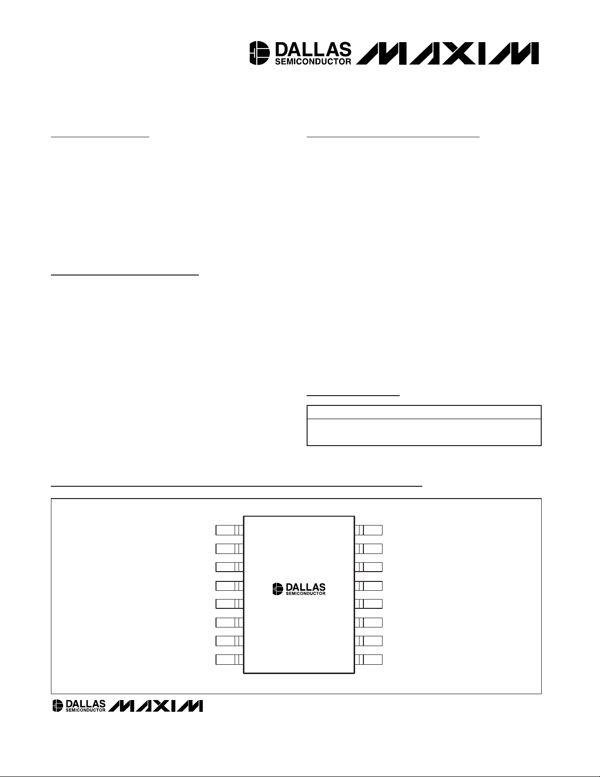
TSSOP (173 mil)
1
2
3
4
5
6
7
89
10
11
12
13
14
15
16L
1
TOP VIEW
W
1
W
2
L
2
I
D1
I
D2
V
D
GND FAULT
A
0
A
1
A
2
SCL
SDA
H
COM
V
CC
DS1870
Pin Configuration
Ordering Information
Rev 1; 5/04
For pricing, delivery, and ordering information, please contact Maxim/Dallas Direct! at
1-888-629-4642, or visit Maxim’s website at www.maxim-ic.com.
PART TEMP RANGE
PIN-PACKAGE
DS1870E-010 -40°C to +95°C
16 TSSOP
(173 mil)
Typical Operating Circuit appears at end of data sheet.
I
2
C is a trademark of Philips Corp. Purchase of I2C components of Maxim Integrated Products, Inc., or one of its sublicensed Associated Companies, conveys a license under the
Philips I
2
C Patent Rights to use these components in an I2C
system, provided that the system conforms to the I
2
C Standard
Specification as defined by Philips.
Page 2
DS1870
LDMOS RF Power-Amplifier Bias
Controller
2 _____________________________________________________________________
ABSOLUTE MAXIMUM RATINGS
RECOMMENDED DC OPERATING CONDITIONS
(TA= -40°C to +95°C)
Stresses beyond those listed under “Absolute Maximum Ratings” may cause permanent damage to the device. These are stress ratings only, and functional
operation of the device at these or any other conditions beyond those indicated in the operational sections of the specifications is not implied. Exposure to
absolute maximum rating conditions for extended periods may affect device reliability.
Voltage Range on VCC, H
COM
, SDA, and SCL Pins Relative to
Ground ...............................................................-0.5V to +6.0V
Voltage Range on A
0
, A1, A2, FAULT, VD, ID1, ID2Relative to
Ground. ...................-0.5V to V
CC
+ 0.5V, not to exceed +6.0V
Voltage Range on L0, L1, W0, and W1 Relative to
Ground .................-0.5V to H
COM
+ 0.5V, not to exceed +6.0V
Operating Temperature Range ...........................-40°C to +95°C
EEPROM Programming Temperature Range .........0°C to +70°C
Storage Temperature Range .............................-55°C to +125°C
Soldering Temperature .......................................See IPC/JEDEC
J-STD-020A Specification
PARAMETER
CONDITIONS
UNITS
Supply Voltage V
CC
(Note 1) 4.5 5.5 V
Input Logic 1
(SDA, SCL, A
2
, A1, A0)
V
IH
0.7 x
V
CC
+
0.3
V
Input Logic 0
(SDA, SCL, A
2
, A1, A0)
V
IL
+0.3 x
V
H
COM
Voltage 4.5 5.5 V
LX and WX Voltage
V
Wiper Current -1 +1 mA
DC ELECTRICAL CHARACTERISTICS
(VCC= +4.5 to 5.5V, TA= -40°C to +95°C.)
PARAMETER
CONDITIONS
Supply Current I
CC
(Note 2) 1 2 mA
Input Leakage I
LI
nA
V
OL1
3mA sink current 0.4 V
Low-Level Output Voltage
(SDA, FAULT)
V
OL2
6mA sink current 0.6 V
I/O Capacitance C
I/O
10 pF
Digital Power-On Reset V
POD
1.0 2.2 V
Analog Power-On Reset V
POA
2.0 2.8 V
SYMBOL
MIN TYP MAX
V
CC
SYMBOL
-0.3
-0.3
MIN TYP MAX UNITS
-200 +200
V
CC
H
COM
+ 0.3
Page 3
DS1870
LDMOS RF Power-Amplifier Bias
Controller
_____________________________________________________________________ 3
ANALOG VOLTAGE-MONITORING CHARACTERISTICS
(VCC= +4.5 to 5.5V, TA = -40°C to +95°C.)
PARAMETER
CONDITIONS
UNITS
VD Monitor FactoryCalibrated FS
Code FFF8h
V
VCC Monitor FactoryCalibrated FS
Code FFF8h
V
ID1 and ID2 Monitor FactoryCalibrated FS
Code FFF8h
V
Resolution
(V
CC
, VD, ID1, ID2)
%FS
Accuracy
(V
CC
, VD, ID1, ID2)
0.5
%FS
Update Rate for
V
CC
, VD, ID1, I
D2
t
frame
50 ms
DIGITAL THERMOMETER CHARACTERISTICS
(VCC= +4.5 to 5.5V, TA= -40°C to +95°C.)
PARAMETER
CONDITIONS
UNITS
Thermometer Error T
ERR
-40°C to 95°C -3 +3 °C
Update Rate t
frame
50 ms
ANALOG POTENTIOMETER CHARACTERISTICS
(VCC= +4.5 to 5.5V, TA= -40°C to +95°C.)
PARAMETER
CONDITIONS
UNITS
Wiper Resistance +25°C
Ω
Potentiometer
End-to-End Resistance
R
POT
+25°C
13
kΩ
Resolution 0.4
%FS
Absolute Linearity (Note 3) -1 +1 LSB
Relative Linearity (Note 4)
LSB
Ratiometric Temperature
Coefficient
5
ppm/°C
End-to-End Temperature
Coefficient
70
ppm/°C
-3dB Cutoff Frequency (Note 5) 1
MHz
Series Resistors from L1, L2 to
GND
R
S
+25°C
kΩ
V
HCOM/VLX
0.6
SYMBOL
SYMBOL
MIN TYP MAX
2.488 2.500 2.513
6.521 6.553 6.587
0.4975 0.5000 0.5025
0.0122
0.25
MIN TYP MAX
SYMBOL
MIN TYP MAX
500 1000
10.0
-0.5 +0.5
15.1 19.5 25.2
0.5975
16.8
0.6025
Page 4
DS1870
LDMOS RF Power-Amplifier Bias
Controller
4 _____________________________________________________________________
LOOKUP TABLE CHARACTERISTICS
(VCC= +4.5 to 5.5V, TA= -40°C to +95°C.)
PARAMETER
CONDITIONS
UNITS
POT1 and POT2 Temp LUT Size
72
Bytes
each
POT1 and POT2 Temp LUT Index
Range
-40
°C
Temp Step 2°C
Temp Hysteresis (Note 6) 1 °C
POT1 and POT2 Drain LUT Size 64
Bytes
each
POT1 and POT2 Drain LUT V
D
Index Range
Hex
POT1 and POT2 Drain LUT V
D
Step
Hex
POT1 and POT2 Drain LUT V
D
Hysteresis
(Note 6)
Hex
POT1 and POT2 Drain LUT I
DX
Index Range
Hex
POT1 and POT2 Drain LUT I
DX
Step
Hex
POT1 and POT2 Drain LUT I
DX
Hysteresis
(Note 6)
Hex
SYMBOL
MIN TYP MAX
+102
8000 FE00
0200
0100
0000 7E00
0200
0100
Page 5
DS1870
LDMOS RF Power-Amplifier Bias
Controller
_____________________________________________________________________ 5
AC ELECTRICAL CHARACTERISTICS
(VCC= +4.5V to 5.5V, TA= -40°C to +95°C, timing referenced to V
IL(MAX)
and V
IH(MIN)
.) (Figure 3)
PARAMETER
CONDITIONS
UNITS
SCL Clock Frequency f
SCL
(Note 7) 0 400 kHz
Bus Free Time Between Stop and
Start Conditions
t
BUF
1.3 µs
Hold Time (Repeated) Start
Condition
0.6 µs
Low Period of SCL t
LOW
1.3 µs
High Period of SCL t
HIGH
0.6 µs
Data Hold Time
0 0.9 µs
Data Setup Time
100 ns
Start Setup Time t
SU:STA
0.6 µs
SDA and SCL Rise Time t
R
(Note 8)
20 +
300 ns
SDA and SCL Fall Time t
F
(Note 8)
20 +
300 ns
Stop Setup Time
0.6 µs
SDA and SCL Capacitive
Loading
C
B
(Note 8) 400 pF
EEPROM Write Time t
W
(Note 9) 10 20 ms
NONVOLATILE MEMORY CHARACTERISTICS
(VCC= +4.5V to 5.5V, TA= 0°C to +70°C.)
PARAMETER
SYMBOL
CONDITIONS
MIN
TYP
MAX
UNITS
Writes +70°C (Note 5)
Note 1: All voltages referenced to ground.
Note 2: Supply current is measured with all logic inputs at their inactive state (SDA = SCL = V
CC
) and driven to well-defined logic
levels. All outputs are disconnected.
Note 3: Absolute linearity is the difference of measured value from expected value at the DAC position. Expected value is a
straight line from measured minimum position to measured maximum position.
Note 4: Relative linearity is the deviation of an LSB DAC setting change vs. the expected LSB change. Expected LSB change is
the slope of the straight line from measured minimum position to measured maximum position.
Note 5: This parameter is guaranteed by design.
Note 6: See Figure 1.
Note 7: I
2
C interface timing shown is for fast-mode (400kHz) operation. This device is also backward compatible with I2C stan-
dard-mode timing.
Note 8: C
B
—total capacitance of one bus line in picofarads.
Note 9: EEPROM write begins after a stop condition occurs.
SYMBOL
t
HD:STA
t
HD:DAT
t
SU:DAT
t
SU:STO
MIN TYP MAX
0.1C
B
0.1C
B
50,000
Page 6
DS1870
LDMOS RF Power-Amplifier Bias
Controller
6 _____________________________________________________________________
Typical Operating Characteristics
(VCC= +5.0V, TA = +25°C, unless otherwise noted.)
POTENTIOMETER 1 AND 2 OUTPUT VOLTAGE
vs. POSITON
DS1870 toc04
WIPER POSITION (DEC)
WIPER VOLTAGE (V)
19212864
1
2
3
4
5
6
0
0 256
H
COM
= 5V
L1 AND L2
NOT CONNECTED
POTENTIOMETER 1 DIFFERENTIAL
NONLINEARITY vs. WIPER POSITION
DS1870 toc05
WIPER POSITION (DEC)
DIFFERENTIAL NONLINEARITY (LSB)
19212864
-0.20
-0.15
-0.10
-0.05
0
0.05
0.10
0.15
0.20
0.25
-0.25
0256
POTENTIOMETER 2 DIFFERENTIAL
NONLINEARITY vs. WIPER POSITION
DS1870 toc06
WIPER POSITION (DEC)
DIFFERENTIAL NONLINEARITY (LSB)
19212864
-0.20
-0.15
-0.10
-0.05
0
0.05
0.10
0.15
0.20
0.25
-0.25
0 256
POTENTIOMETER 1 INTEGRAL
NONLINEARITY vs. WIPER POSITION
DS1870 toc07
WIPER POSITION (DEC)
INTEGRAL NONLINEARITY (LSB)
19212864
-0.4
-0.3
-0.2
-0.1
0
0.1
0.2
0.3
0.4
0.5
-0.5
0 256
POTENTIOMETER 2 INTEGRAL
NONLINEARITY vs. WIPER POSITION
DS1870 toc08
WIPER POSITION (DEC)
INTEGRAL NONLINEARITY (LSB)
19212864
-0.4
-0.3
-0.2
-0.1
0
0.1
0.2
0.3
0.4
0.5
-0.5
0256
POTENTIOMETER 1 AND 2
WIPER RESISTANCE vs. WIPER VOLTAGE
DS1870 toc09
WIPER VOLTAGE (V)
WIPER RESISTANCE (Ω)
4321
100
200
300
400
500
600
700
800
900
1000
0
05
H
COM
= 5.0V
SUPPLY CURRENT vs. SUPPLY VOLTAGE
DS1870 toc01
SUPPLY VOLTAGE (V)
SUPPLY CURRENT (mA)
5.35.14.94.7
620
640
660
680
700
720
740
760
780
800
600
4.5 5.5
SUPPLY CURRENT vs. TEMPERATURE
DS1870 toc02
TEMPERATURE (°C)
SUPPLY CURRENT (mA)
806020 400-20
450
500
550
600
650
700
750
800
850
900
400
-40 100
VCC = 5.5V
VCC = 4.5V
VCC = 5.0V
H
COM
CURRENT vs. H
COM
VOLTAGE
DS1870 toc03
H
COM
VOLTAGE (V)
H
COM
CURRENT (mA)
5.35.14.94.7
0.05
0.10
0.15
0.20
0.25
0.30
0.35
0.40
0.45
0.50
0
4.5 5.5
Page 7
DS1870
LDMOS RF Power-Amplifier Bias
Controller
_____________________________________________________________________ 7
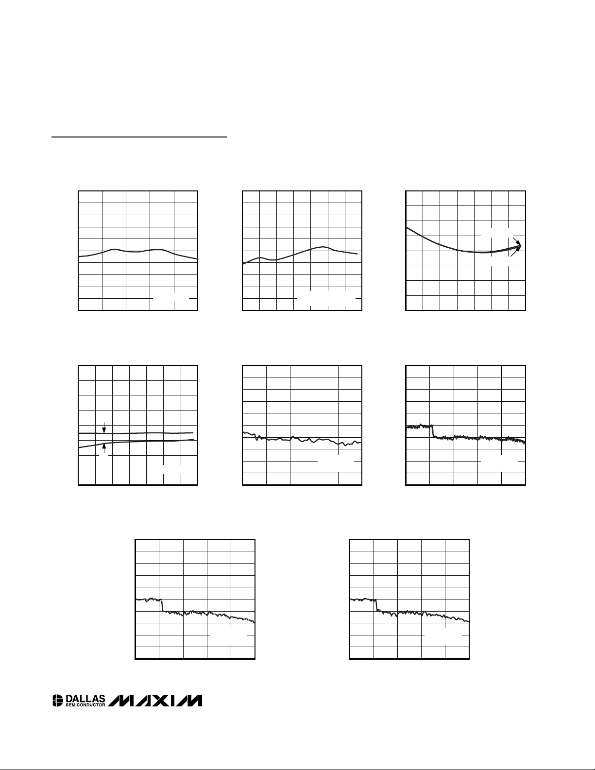
Typical Operating Characteristics (continued)
(VCC= +5.0V, TA = +25°C, unless otherwise noted.)
OUTPUT DRIFT (PPM/C)
-15
-10
-5
0
5
10
15
20
-20
POTENTIOMETER LOW TERMINAL VOLTAGE
vs. TEMPERATURE
DS1870 toc12
TEMPERATURE (°C)
8060-20 0 20 40-40 100
L1
L2
H
COM
= 5.0V
VCC CONVERSION ERROR
vs. SUPPLY VOLTAGE
DS1870 toc13
SUPPLY VOLTAGE (V)
ERROR (% FS)
5.04.54.03.5
-0.4
-0.3
-0.2
-0.1
0
0.1
0.2
0.3
0.4
0.5
-0.5
3.0 5.5
DEFAULT V
CC
CALIBRATION
VD CONVERSION ERROR
vs. INPUT VOLTAGE
DS1870 toc14
INPUT VOLTAGE (V)
ERROR (% FS)
2.01.51.00.5
-0.4
-0.3
-0.2
-0.1
0
0.1
0.2
0.3
0.4
0.5
-0.5
0 2.5
DEFAULT VD
CALIBRATION
ID1 CONVERSION ERROR
vs. INPUT VOLTAGE
DS1870 toc15
INPUT VOLTAGE (V)
ERROR (% FS)
0.40.30.20.1
-0.4
-0.3
-0.2
-0.1
0
0.1
0.2
0.3
0.4
0.5
-0.5
0 0.5
DEFAULT ID1
CALIBRATION
ID2 CONVERSION ERROR
vs. INPUT VOLTAGE
DS1870 toc16
INPUT VOLTAGE (V)
ERROR (% FS)
0.40.30.20.1
-0.4
-0.3
-0.2
-0.1
0
0.1
0.2
0.3
0.4
0.5
-0.5
0 0.5
DEFAULT ID2
CALIBRATION
POTENTIOMETER 1 AND 2
WIPER RESISTANCE vs. WIPER VOLTAGE
DS1870 toc09
WIPER VOLTAGE (V)
WIPER RESISTANCE (Ω)
4321
100
200
300
400
500
600
700
800
900
1000
0
05
H
COM
= 5.0V
POTENTIOMETER 1 AND 2
WIPER RESISTANCE vs. TEMPERATURE
DS1870 toc10
TEMPERATURE (°C)
RESISTANCE CHANGE FROM 25°C (PPM/C)
806020 400-20
100
200
300
400
500
600
700
800
900
1000
0
-40 100
H
COM
= 5V
WIPER VOLTAGE = 4V
POTENTIOMETER END-TO-END RESISTANCE
vs. TEMPERATURE
DS1870 toc11
TEMPERATURE (°C)
CHANGE FROM RESISTANCE AT 25°C (PPM/C)
8060-20 0 20 40
-150
-100
-50
0
50
100
150
200
-200
-40 100
R
POT2
+ R
S2
R
POT1
+ R
S1
Page 8
DS1870
LDMOS RF Power-Amplifier Bias
Controller
8 _____________________________________________________________________
Pin Description
PIN NAME FUNCTION
1L1Potentiometer 1 Low Terminal
2W1Potentiometer 1 Wiper Terminal
3W2Potentiometer 2 Wiper Terminal
4L2Potentiometer 2 Low Terminal
5ID1Drain Current 1 Monitor Input
6ID2Drain Current 2 Monitor Input
7VDDrain Voltage Monitor Input
8 GND Ground
9 FAULT
Fault Output. This open-collector output is active high when one of the enabled alarms is outside its
programmable limit value.
10 A
0
11 A
1
12 A
2
I2C Address Inputs. These inputs determine the slave address of the device. The slave address in
binary is 1010A
2A1A0
.
13 SCL Serial Clock Input. I2C clock input.
14 SDA Serial Data Input/Output. Bidirectional I2C data pin.
15 H
COM
Potentiometer High Terminal. Common to potentiometers 1 and 2.
16 V
CC
Power Input
Page 9
DS1870
LDMOS RF Power-Amplifier Bias
Controller
_____________________________________________________________________ 9
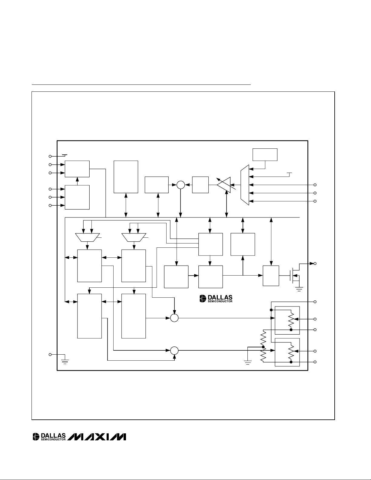
Functional Diagram
∑
∑
+
+
+
+
∑
++
M
U
X
13-BIT
ADC
ON-CHIP
TEMP SENSOR
V
CC
V
D
I
D1
I
D2
ADDRESS
GENERATION
SDA
SCL
A
0
A
1
A
2
I2C DATA BUS
32 BYTES
USER
MEMORY
OFFSET
CALIBRATION
REGISTERS
FAULT
LOAD
INDEX
INDEX
INDEX
INDEX
LOAD
TEMP
POT1
R
POT
POT2
R
POT
H
COM
L
2
W
2
W
1
L
1
POT1
DRAIN
LUT
TABLE 4
(64 BYTES)
POT2
DRAIN
LUT
TABLE 5
(64 BYTES)
LIMIT
COMPARATOR
LIMIT FLAG
REGISTERS
FAULT
MASK
V
CC
V
CC
GND
GAIN
CALIBRATION
REGISTERS
V
D
VD1
VD2
V
D
I
D2
I
D1
POT1
TEMP
LUT
TABLE 2
(72 BYTES)
POT2
TEMP
LUT
TABLE 3
(72 BYTES)
R
S
R
S
I
2
C INTERFACE
CONTROL
HI AND LO
LIMITS FOR
TEMP, V
CC
,
V
D
, ID1, I
D2
MEASURED
VALUES FOR
TEMP, V
CC
,
V
D
, ID0, I
D1
DS1870
Page 10

DS1870
LDMOS RF Power-Amplifier Bias
Controller
10 ____________________________________________________________________
Detailed Description
The DS1870 is a dual-channel LDMOS bias controller.
It is intended to replace traditional bias control solutions that are limited by a constant temperature-coefficient correction. This IC offers lookup table correction
that is programmable as a function of temperature as
well as drain supply voltage or current. The flexibility to
use a nonlinear bias correction improves efficiency significantly. This is a direct consequence of the ability to
lower the bias current, particularly in class AB operation, since the bias correction no longer requires a constant temperature coefficient. In addition, correcting the
bias as a function of drain supply voltage, or drain current in class AB, assists in distortion reduction and gain
management.
Two outputs (W1 and W2), each controlled by a dedicated two-dimensional lookup table as shown in the
functional diagram, drive two LDMOS gates. The two
degrees of freedom are temperature and either drain
supply voltage or drain current. The lookup tables are
programmed during power-amplifier assembly and
test. After calibration, the IC automatically recalls the
proper control setting for each output, based on temperature and drain characteristics.
A 13-bit ADC samples and digitizes the chip temperature, VCC, the drain supply voltage, and two drain currents. These digitized signals are stored in memory
ready to be accessed by the look up table controls.
The digitized values are also compared to alarm
thresholds generating high or low alarm flags. The
FAULT output can be configured to assert high based
any alarm’s assertion, or the alarms can be masked to
prevent unwanted fault assertions. The ADC readings
as well as the alarm flags and fault status are accessible through the I2C-compatible interface.
Voltage/Current Monitor Operation
The DS1870 monitors four voltages (VCC, VD, ID1, and
ID2) plus the temperature in a round-robin fashion using
its 13-bit ADC. The converted voltage values are stored
in memory addresses 62h–69h as 16-bit unsigned
numbers with the ADC result left justified in the register.
The three least significant bits of the ADC result registers
are masked to zero. The round-robin time is specified by
t
frame
in the analog voltage-monitoring characteristics.
The default factory-calibrated values for the voltage
monitors are shown in Table 1.
To calculate the voltage measured from the register
value, first calculate the LSB weight of the 16-bit register that is equal to the full-scale voltage span divided
by 65,528. Next, convert the hexadecimal register
value to decimal and multiply it times the LSB weight.
Example: Using the factory default VCCtrim, what voltage is measured if the V
CC
register value is C347h?
The LSB for V
CC
is equal to (6.553V - 0V) / 65,528 =
100.00µV. C347h is equal to 49,991 decimal, which
yields a supply voltage equal to 49,991 x 100.00µV =
4.999V. Table 2 shows more conversion examples
based on the factory trimmed ADC settings.
By using the internal gain and offset calibration registers, the +FS and -FS signal values shown in Table 1
can be modified to meet customer needs. For more
information on calibration, see the Voltage/Temperature
Monitor Calibration section.
Note: The method shown above for determining the
input voltage level only works when the offset register is
set to zero.
SIGNAL
+FS SIGNAL
+FS
(hex)
-FS
-FS
(hex)
V
CC
6.553V FFF8 0V 0000
V
D
2.5V FFF8 0V 0000
I
D1
0.5V FFF8 0V 0000
I
D2
0.5V FFF8 0V 0000
Table 1. Voltage-Monitor Factory Default
Calibration
SIGNAL
LSB
REGISTER
INPUT
VOLTAGE (V)
V
CC
100.00 8080 3.29
V
CC
100.00 C0F8 4.94
V
D
38.152 C000 1.875
V
D
38.152 8080 1.255
I
D1
7.6303 8000 0.2500
I
D2
7.6303 1328 0.0374
Table 2. Voltage-Monitor Conversion
Examples
SIGNAL
WEIGHT (µV)
VALUE (hex)
Page 11

DS1870
LDMOS RF Power-Amplifier Bias
Controller
____________________________________________________________________ 11
Temperature-Monitor Operation
The internal temperature monitor values are stored as
16-bit 2’s complement numbers at memory addresses
60h to 61h. The round-robin update time (t
frame
) for the
temperature register is the same as the voltage monitors. The factory default calibration values for the temperature monitor are shown in Table 3.
To convert the 2’s complement register value to the
temperature it represents, first convert the 2-byte hexadecimal value to a decimal value as if it is an unsigned
value, then divide the result by 256. Finally, subtract
256 if the result of the division is greater than or equal
to +128. Table 4 shows example converted values.
The offset of the temperature sensor can be adjusted
using the internal calibration registers to account for
differences between the ambient temperature at the
location of the DS1870 and the temperature of the
device it is biasing. When offsets are applied to the
temperature measurement, the value converted will be
off by a fixed value from the DS1870’s ambient temperature. For more information, see the Temperature
Monitor Offset Calibration section.
Potentiometer Operation
Both of the DS1870’s potentiometers are 256 positions
with their high terminals connected to the high common
pin, H
COM
. The low terminals of the potentiometers are
internally shunted to GND by resistors such that the
output voltage is 3V to 5V when H
COM
is connected to
a 5V source. The internal shunt resistors and the potentiometer’s end-to-end resistance feature matching temperature coefficients that prevent the output voltage
from drifting over temperature.
External resistors can be placed from H
COM
to LXand/or
from LXto GND to modify the typical output voltage.
Normal Operation
During normal operation, each potentiometer’s position
is automatically adjusted to the sum of its temperature
and drain LUT values after each round of conversions.
The potentiometer setting is applied after both the base
and offset LUT values are recalled from memory. The
sum of the currently indexed values in the POT1 Temp
LUT (memory table 2) and the POT1 Drain LUT (memory table 4) control potentiometer 1. The sum of the currently indexed values in the POT2 Temp LUT (memory
table 3) and the POT2 Drain LUT (memory table 5) control potentiometer 2. In the event that two table values
are summed and the result is greater than 255 or less
than 0, the potentiometer’s position is set to 255 or 0,
respectively.
SIGNAL
+FS
+FS
(hex)
-FS
-FS
(hex)
Temp
7FF8
8000
Table 3. Internal Temperature-Monitor
Factory Default Calibration
MSB
(bin)
LSB
(bin)
TEMPERATURE
(°C)
01000000 00000000 +64
01000000 00001111 +64.059
01011111 00000000 +95
11110110 00000000 -10
11011000 00000000 -40
Table 4. Temperature Conversion Values
LUT ADDRESS (hex)
CORRESPONDING
TEMPERATURE (°C)
80 ≤ -40°C
81 -38°C
82 -36°C
……
C6 +100°C
C7 ≥ +102°C
Table 5. LUT Addresses for
Corresponding Temperature Values
SIGNAL
+127.97°C
SIGNAL
-128.00°C
Page 12

DS1870
LDMOS RF Power-Amplifier Bias
Controller
12 ____________________________________________________________________
The temperature tables (LUT 2 and LUT 3) are 72 bytes
each. This allows the biasing to be adjusted every 2°C
between -40°C and +102°C. Temperatures less than
-40°C or greater than 102°C use the -40°C or 102°C
values, respectively. The values in the temperature
tables are 8-bit unsigned values (0 to 255 decimal) that
allow the potentiometer to be set to any position as a
function of the temperature. The temperature LUTs
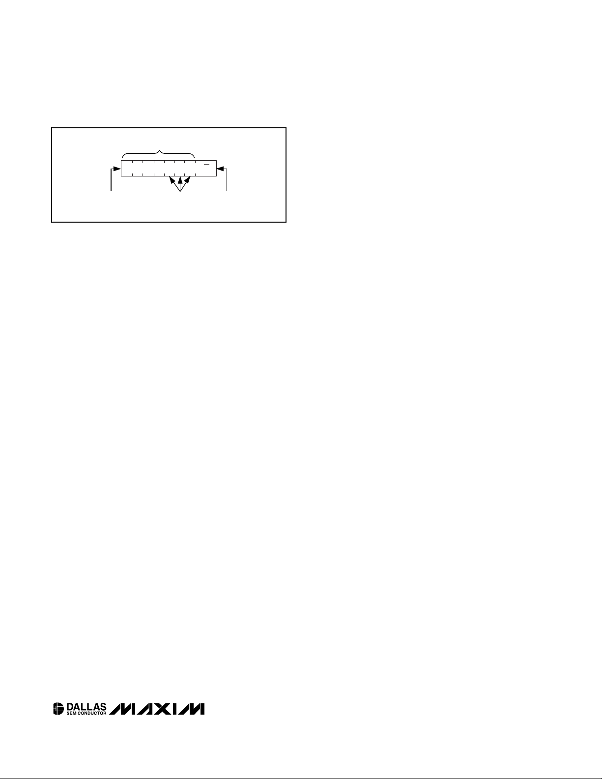
have 1°C hysteresis (Figure 1) to prevent the potentiometer’s position from chattering in the event the temperature remains near a LUT switching point. Table 5
shows how the DS1870 determines the temperature
tables index as a function of temperature.
The drain tables (LUT 4 and LUT5) are 64 bytes each,
and they can be indexed either by the drain voltage or
the drain current corresponding to the potentiometer.
The VD1 control bit determines if the voltage sensed on
VDor ID1adjusts the POT1 Drain LUT, and the VD2
control bit determines if the voltage sensed on VDor
I
D2
controls the POT2 Drain LUT. The VD1 and VD2
control bits are located in register 85h of memory table
1. The drain tables are programmed with an 8-bit
signed value (-128 to +127 decimal) that allow a relative offset from the temperature LUT values determined
by the amplifier’s drain characteristics.
The drain LUTs are indexed either by the upper half of
the V
D
range or the lower half of its corresponding I
DX
range. Table 6 shows how the index is determined
based on the VDor IDXvalues. Hysteresis equal to
0100h is also implemented on the drain monitor
(Figure 1) to ensure that voltages close to a switching
point do not cause the potentiometer position to chatter
between two LUT values. The drain LUT index values are
specified in hexadecimal because the hexadecimal values are applicable regardless of the gain and offset calibration of the DS1870.
Manual Mode
During normal operation, the potentiometer position is
automatically modified once per conversion cycle
based on the ADC results. The DS1870 can either stop
the update function all together by using the B/O_en
bit, or the temperature and drain LUT indexes can be
manually controlled by using the Index_en bit. These
bits are located in the Man DAC register located in
memory table 1, byte AFh. More information about
these bits is in the Register Description section.
Voltage-Monitor Calibration
The DS1870 can scale each analog voltage’s gain and
offset to produce the desired digital result. Each of the
inputs (VCCVD, ID1, ID2) has a unique register for the
gain and offset (in memory table 1) allowing them to be
individually calibrated. Additionally, the DS1870 offers
the ability to provide a temperature offset to allow the
temperature measurement to be compensated to
account for the difference in temperature between the
DS1870 and the device it is biasing.
To scale the gain and offset of the converter for a specific input, you must first know the relationship between
the analog input and the expected digital result. The
input that would produce a digital result of all zeros is
the null value (normally this input is GND). The input
that would produce a digital result of all ones (FFF8h) is
LUT ADDRESS
(hex)
V
D
VALUE
(hex)
IDX VALUE
(hex)
80 ≤ 8000 0000
81 8200 0200
82 8400 0400
…… …
BE FC00 7C00
BF ≥ FE00 ≥ 7E00
Table 6. LUT Addresses for VDor I
DX
Values
9Ah
99h
98h
97h
96h
95h
246 810 12
TEMPERATURE (°C)
MEMORY LOCATION
MEMORY LOCATION
MEMORY LOCATION
9Ah
99h
98h
97h
96h
95h
AA00 AC00 AEOO B000 B200 B400
DRAIN VOLTAGE CONVERSION (HEX)
9Ah
99h
98h
97h
96h
95h
2A00 2C00 2E00 3000 3200 3400
DRAIN CURRENT CONVERSION (HEX)
INCREASING
TEMPERATURE
INCREASING
DRAIN VOLTAGE
INCREASING
DRAIN CURRENT
DECREASING
TEMPERATURE
DECREASING
DRAIN VOLTAGE
DECREASING
DRAIN CURRENT
Figure 1. LUT Hysteresis
Page 13

DS1870
LDMOS RF Power-Amplifier Bias
Controller
____________________________________________________________________ 13
the full-scale (FS) value. The expected FS value is also
found by multiplying an all-ones digital answer by the
LSB weight.
Example: Since the FS digital reading is 65,528 (FFF8
hex) LSBs, if the LSB’s weight is 50µV, then the FS
value is 65,528 x 50µV = 3.2764V.
A binary search is used to calibrate the gain of the converter. This requires forcing two known voltages to the
input pin. It is preferred that one of the forced voltages
is the null input and the other is 90% of FS. Since the
LSB of the least significant bit in the digital reading register is known, the expected digital results can be calculated for both the null input and the 90% of full scale
value.
An explanation of the binary search used to scale the
gain is best served with the following example pseudocode:
/* Assume that the null input is 0.5V */
/* Assume that the requirement for the LSB is 50µV */
FS = 65528 * 50e-6; /*3.2764V */
CNT1 = 0.5 / 50e-6; /* 1000 */
CNT2 = 0.9 X FS / 50e-6; /* 58981.5 */
/* So the null input is 0.5V and 90% of FS is 2.949V */
Set the input’s offset register to zero
gain_result = 0h; /* Working register for gain
calculation */
CLAMP = FFF8h; /* This is the max ADC value*/
For n = 15 down to 0
begin
gain_result = gain_result + 2
n
;
Write gain_result to the input’s
gain register;
Force the 90% FS input (2.949V);
Meas2= ADC result from DS1870;
If Meas2 ≥ CLAMP
Then
gain_result = gain_result - 2
n
;
Else
Force the null input (0.5V)
Meas1 = ADC result from DS1870
If [(Meas2-Meas1)>(CNT2-CNT1)]
Then
gain_result = gain_result - 2
n
;
end;
Write gain_result to the input’s gain
register;
The gain register is now set and the resolution of the
conversion matches the expected LSB. Customers
requiring non-zero null values (e.g., 0.5V) must next
calibrate the input’s offset. If the desired null value is
0V, leave the offset register programmed to 0000h and
skip this step.
To calibrate the offset register, program the gain register with the gain_result value determined above. Next,
force the null input voltage (0.5V for the example) and
read the digital result from the part (Meas1). The offset
value can be calculated using the following formula:
Temperature-Monitor Offset Calibration
The DS1870’s temperature sensor comes precalibrated
and requires no further adjustment by the customer for
proper operation. However, it is possible for customers
to characterize their system and add a fixed offset to
the DS1870’s temperature reading so it is reflective of
another location’s temperature. This is not required for
biasing because the temperature offset can be
accounted for by adjusting the data’s location in the
LUTs, but this feature is available for customers who
see application benefits.
To change the temperature sensor’s offset: write the
temperature offset register to 0000h, measure the
source reference temperature (T
ref
), and read the tem-
perature from the DS1870 (T
DS1870
). Then, the following formula can be used to calculate the value for the
temperature offset register.
Once the value is calculated, write it to the temperature
offset register.
Power-Up and Low-Voltage Operation
During power-up, the device is inactive until V
CC
exceeds the digital power-on-reset voltage (V
POD
). At
this voltage, the digital circuitry, which includes the I2Ccompatible interface, becomes functional. However,
EEPROM-backed registers/settings cannot be internally
read (recalled) until VCCexceeds the analog power-on
reset (V
POA
), at which time the remainder or the device
becomes fully functional. Once V
CC
exceeds V
POA
, the
Rdyb bit in byte 74h is timed to go from a 1 to a 0 and
indicates when ADC conversions begin. If V
CC
ever
dips below V
POA
, the Rdyb bit reads as a 1 again.
Once a device exceeds V
POA
and the EEPROM is
recalled, the values remain active (recalled) until V
CC
falls below V
POD
.
TempOffset T T XOR BB h
ref DS bitwise
=×− + −
()
()
64 275 40
1870
Offset
Meas
= − ×
1
1
4
Page 14

DS1870
LDMOS RF Power-Amplifier Bias
Controller
14 ____________________________________________________________________
As the device powers up, the VCCLO alarm flag
defaults to a 1 until the first VCCADC conversion
occurs and sets or clears the flag accordingly. The
FAULT output is active when VCC< V
POA
.
Memory Description
The DS1870 memory map is divided into six sections
that include the lower memory (addresses 00h to 7Fh)
and five memory tables (Figure 2). The memory tables
are addressed by setting the table-select byte (7Fh) to
the desired table number and accessing the upper
memory locations (80h to FFh). The lower memory can
be addressed at any time regardless of the state of the
table-select byte. The lower memory and memory table
1 are used to configure the DS1870 and read the status
of the monitors. The lower memory also contains the 32
bytes of user memory. Memory tables 2 and 3 contain
the base potentiometer positions that are used for biasing based on the reading of the internal temperature
sensor. Memory tables 4 and 5 contain the relative offsets that are added to the base number as a function of
either the drain voltage or the individual drain current
monitors. See the Memory Map for a complete listing of
registers and the Register Description section for
details about each register.
Password Memory Protection
The DS1870 contains a 2-byte password that allows all
of its EE memory to be write protected until the proper
password is entered into the password entry (PWE)
word (address 78h). This allows factory calibration data
for the bias settings, alarm thresholds, and all the other
EEPROM information to be write protected. The password is set by writing to the Password register, which is
the first two bytes of memory table 1.
The factory default value for the password is FFFFh,
which is also the factory default value for PWE on
power-up. This means that parts are unlocked at
power-up when they are first received by customers.
The password should be programmed to a value other
than FFFFh to ensure the calibration data is write protected. The PWE register always reads 0000h regardless of its programmed value.
EEPROM Write Disable
Memory locations 20h to 3Fh and Table 1 locations 80h
to A7h are SRAM-shadowed EEPROM. By default
(SEE = 0) these locations act as ordinary EEPROM. By
setting SEE = 1, these locations begin to function like
SRAM cells, which allow an infinite number of write
cycles without concern of wearing out the EEPROM.
This also eliminates the requirement for the EEPROM
write time. Because changes made with SEE = 1 do not
affect the EEPROM, these changes are not retained
through power cycles. The power-up value is the last
value written with SEE = 0. This function can be used to
limit the number of EEPROM writes during calibration or
to change the monitor thresholds periodically during
normal operation without wearing out the EEPROM. The
SEE bit resides in memory table 1, byte AFh.
Memory Map
The upper part of the memory map is organized into
8-byte or 4-word (2-byte) rows. The beginning address
of the row is shown in the left-most column of the map,
and is equal to the byte 0 or word 0 memory address.
The next byte (Byte 1) is located at the next highest
memory address, and the next word (Word 1) is two
memory addresses greater than the row’s beginning
address. The lower part of the memory map expands
the bytes or the words to show the names of the bits
within the byte/word, or their bit weights (2X) for registers that contain numerical information. Numerical registers that contain an “S” in the most significant bit are
showing sign extension for 2’s complement numbers.
Descriptions of each byte/bit follow in the Register
Description section.
USER MEMORY;
HI/LO ALARM
THRESHOLDS;
ADC RESULTS;
CONFIGURATION
CONFIGURATION
POT1
TEMP
LUT
POT2
TEMP
LUT
POT1
DRAIN
LUT
POT2
DRAIN
LUT
00h
7Fh
80h
AFh
80h
C7h
80h
C7h
80h
BFh
80h
BFh
MAIN MEMORY
TABLE 1 TABLE 2 TABLE 3 TABLE 4 TABLE 5
TABLE-SELECT
BYTE (7Fh)
SEL
SEL SEL
SEL SEL
Figure 2. Memory Organization
Page 15

DS1870
LDMOS RF Power-Amplifier Bias
Controller
____________________________________________________________________ 15
LOWER MEMORY
WORD 0 WORD 1 WORD 2 WORD 3
ROW
(HEX)
ROW
NAME
BYTE 0 BYTE 1 BYTE 2 BYTE 3
BYTE 6
BYTE 7
00
User EE User EE
User EE
User EE
User EE
08
User EE User EE
User EE
User EE
User EE
10
User EE User EE
User EE
User EE
User EE
18
User EE User EE
User EE
User EE
User EE
20
Temp Hi Alarm VCC Hi Alarm VD Hi Alarm ID1 Hi Alarm
28
ID2 Hi Alarm Reserved Reserved Reserved
30
Temp Lo Alarm VCC Lo Alarm VD Lo Alarm ID1 Lo Alarm
38
ID2 Lo Alarm Reserved Reserved Reserved
40
Reserved
48
Reserved
50
Reserved
58
Reserved
60
Temp Value VCC Value VD Value ID1 Value
68
ID2 Value Reserved Reserved Reserved
70 Status
Lo Alarm
Reserved
78
PWE
Tbl Sel
EXPANDED BYTES
BIT 7 BIT 6 BIT 5 BIT 4 BIT 3 BIT 2 BIT 1 BIT 0
BYTE
(HEX)
BYTE
NAME
BIT000-1F
User EE EE EE EE EE EE EE EE EE
20
S
2
2
2
-8
22
2
0
24
2
0
26
2
0
28
2
0
30
S
2
2
2
-8
32
2
0
34
2
0
36
2
0
38
2
0
60
S
2
2
2
-8
62
2
0
64 VD Value
2
0
66 ID1 Value
2
0
68 ID2 Value
2
0
70 Hi Alarm Temp Hi VCC Hi VD Hi ID1 Hi ID2 Hi
Reserved
71 Lo Alarm Temp Lo VCC Lo VD Lo ID1 Lo ID2 Lo
Reserved
74 I/O Status
Fault Mint
Rdyb
75
VD Rdy
ID2 Rdy
Reserved
78 PWE 2
15
2
0
7F Tbl Sel 2
7
2
6
2
5
2
4
2
3
2
2
2
1
2
0
User Row
User Row
User Row
User Row
Threshold
Threshold
Threshold
Threshold
A2D Value
A2D Value
Table Select
0
1
2
3
0
1
2
3
Reserved Reserved Reserved Reserved Reserved Reserved Reserved
Reserved Reserved Reserved Reserved Reserved Reserved Reserved
Reserved Reserved Reserved Reserved Reserved Reserved Reserved
Reserved Reserved Reserved Reserved Reserved Reserved Reserved
0
1
Hi Alarm
Temp Hi Alrm
VCC Hi Alrm 2
VD Hi Alrm 2
ID1 Hi Alrm 2
ID2 Hi Alrm 2
Temp Lo Alrm
VCC Lo Alrm 2
VD Lo Alrm 2
ID1 Lo Alrm 2
ID2 Lo Alrm 2
Temp Value
VCC Value 2
BIT15BIT14BIT13BIT12BIT11BIT10BIT9BIT8BIT7BIT6BIT5BIT4BIT3BIT2BIT
2
2
2
6
2
15
2
15
2
15
2
15
2
2
15
2
15
2
15
2
15
2
2
15
2
15
2
15
2
15
2
5
2
14
13
2
14
13
2
14
13
2
14
13
2
6
5
2
14
13
2
14
13
2
14
13
2
14
13
2
6
5
2
14
13
2
14
13
2
14
13
2
14
13
2
Reserved Reserved Reserved Reserved
A2D Status Temp Rdy VCC Rdy
14
2
13
2
User EE
User EE
User EE
User EE
Reserved Reserved I/O Status A2D Status Reserved
Reserved Reserved Reserved Reserved Reserved
4
2
2
2
2
2
2
2
2
2
2
2
2
2
2
2
3
2
12
11
2
12
12
12
4
12
12
12
12
4
12
12
12
12
2
11
2
2
11
2
2
11
2
2
3
2
11
2
2
11
2
2
11
2
2
11
2
2
3
2
11
2
2
11
2
2
11
2
2
11
2
2
1
2
10
9
2
10
9
2
10
9
2
10
9
2
1
2
10
9
2
10
9
2
10
9
2
10
9
2
1
2
10
9
2
10
9
2
10
9
2
10
9
2
ID1 Rdy
12
11
2
2
10
2
2
BYTE 4 BYTE 5
User EE User EE
User EE User EE
User EE User EE
User EE User EE
0
8
8
8
8
0
8
8
8
8
0
8
8
8
8
282
-1
2
7
2
7
2
7
2
7
2
-1
2
7
2
7
2
7
2
7
2
-1
2
7
2
7
2
7
2
7
2
7
2
2
2
2
2
2
2
2
2
2
2
2
2
2
2
9
2-22-32-42-52-62
26252423222
26252423222
26252423222
26252423222
2-22-32-42-52-62
26252423222
26252423222
26252423222
26252423222
2-22-32-42-52-62
26252423222
26252423222
26252423222
26252423222
Reserved Reserved
Reserved Reserved
Reserved
Reserved Reserved
26252423222
1
-7
1
1
1
1
-7
1
1
1
1
-7
1
1
1
1
1
Page 16
DS1870
LDMOS RF Power-Amplifier Bias
Controller
16 ____________________________________________________________________
TABLE 1 ( CONFIGURATION )
WORD 0 WORD 1 WORD 2 WORD 3
ROW
(HEX)
ROW
BYTE 0 BYTE 1 BYTE 2 BYTE 3
BYTE 6 BYTE 7
80
Password
Fault Ena Reserved
88
Reserved Vcc Scale VD Scale ID1 Scale
90
ID2 Scale Reserved Reserved Reserved
98
Reserved Vcc Offset VD Offset ID1 offset
A0
ID2 Offset Reserved Reserved Temp Offset
A8
LUT
T Index
POT2
base
POT2 off Man Dac
EXPANDED BYTES
BIT 7 BIT 6 BIT 5 BIT 4 BIT 3 BIT 2 BIT 1 BIT 0
BYTE
(HEX)
BYTE
BIT
0
80
2
3
2
2
2
1
2
0
85
Reserved
VD2 VD1
86
Vcc Ena VD Ena
Reserved Reserved
8A
Vcc
2
3
2
2
2
1
2
0
8C
2
3
2
2
2
1
2
0
8E
2
3
2
2
2
1
2
0
90
2
3
2
2
2
1
2
0
9A
Vcc
Offset
2
5
2
4
2
3
2
2
9C
2
5
2
4
2
3
2
2
9E
ID1
2
5
2
4
2
3
2
2
A0
ID2
2
5
2
4
2
3
2
2
A6
Temp
Offset
2
5
2
-3
2
-4
2
-5
2
-6
A8
2
7
2
6
2
5
2
4
2
3
2
2
2
1
2
0
A9
2
7
2
6
2
5
2
4
2
3
2
2
2
1
2
0
AA
2
7
2
6
2
5
2
4
2
3
2
2
2
1
2
0
AB
POT1
base
2
7
2
6
2
5
2
4
2
3
2
2
2
1
2
0
AC
S262
5
2
4
2
3
2
2
2
1
2
0
AD
POT2
base
2
7
2
6
2
5
2
4
2
3
2
2
2
1
2
0
AE
S262
5
2
4
2
3
2
2
2
1
2
0
AF
Reserved
SEE B/O_en index_en
NAME
Config
Scale
0
Scale
1
Offset
0
Offset
1
Index
NAME
Password 2
LUT Sel Reserved Reserved
Fault Ena Temp Ena
VD Scale 2
ID1 Scale 2
ID2 Scale 2
BIT
BIT14BIT13BIT12BIT11BIT10BIT9BIT8BIT7BIT6BIT5BIT4BIT3BIT2BIT
15
15
15
2
15
15
15
SS2152
VD Offset S S 2
SS2152
SS2152
S282
T Index
O1 Index
O1 Index O2 Index POT1 base POT1 off
14
13
12
11
10
2
2
2
2
2
9
2
Reserved Reserved Reserved
ID1 Ena ID2 Ena Reserved
14
13
12
11
10
2
2
2
2
14
13
2
2
14
2
2
14
2
2
12
2
13
12
2
13
12
2
14
15
14
2
14
14
7
6
2
2
11
2
2
11
2
2
11
2
2
13
2
2
13
2
2
13
2
2
13
2
2
2
9
2
10
9
2
10
9
2
10
9
2
12
11210
2
12
11210
2
12
11210
2
12
11210
2
4
3
2
O2 Index
POT1 off
POT2 off
Man DAC Reserved Reserved
Reserved Reserved
BYTE 4 BYTE 5
LUT Sel
8
2
2726252
4
8
2
2726252
8
2
2726252
8
2
2726252
8
2
2726252
2928272
2928272
2928272
2928272
2
2
21202-12
4
4
4
4
6
6
6
6
-2
1
Page 17

DS1870
LDMOS RF Power-Amplifier Bias
Controller
____________________________________________________________________ 17
TABLE 2 (POT1 TEMP LUT)
WORD 0 WORD 1 WORD 2 WORD 3
ROW
(HEX)
ROW
NAME
BYTE 0 BYTE 1 BYTE 2 BYTE 3 BYTE 4 BYTE 5 BYTE 6 BYTE 7
80 LUT POT1 POT1 POT1 POT1 POT1 POT1 POT1 POT1
88 LUT POT1 POT1 POT1 POT1 POT1 POT1 POT1 POT1
90 LUT POT1 POT1 POT1 POT1 POT1 POT1 POT1 POT1
98 LUT POT1 POT1 POT1 POT1 POT1 POT1 POT1 POT1
A0 LUT POT1 POT1 POT1 POT1 POT1 POT1 POT1 POT1
A8 LUT POT1 POT1 POT1 POT1 POT1 POT1 POT1 POT1
B0 LUT POT1 POT1 POT1 POT1 POT1 POT1 POT1 POT1
B8 LUT POT1 POT1 POT1 POT1 POT1 POT1 POT1 POT1
C0 LUT POT1 POT1 POT1 POT1 POT1 POT1 POT1 POT1
C8
Reserved
D0
Reserved
D8
Reserved
E0
Reserved
E8
Reserved
F0
Reserved
F8
Reserved
EXPANDED BYTES
BYTE
(HEX)
BYTE
BIT 7 BIT 6 BIT 5 BIT 4 BIT 3 BIT 2 BIT 1 BIT 0
80-C7
POT1 2
7
2
6
2
5
2
4
2
3
2
2
2
1
2
0
Reserved Reserved Reserved Reserved Reserved Reserved Reserved
Reserved Reserved Reserved Reserved Reserved Reserved Reserved
Reserved Reserved Reserved Reserved Reserved Reserved Reserved
Reserved Reserved Reserved Reserved Reserved Reserved Reserved
Reserved Reserved Reserved Reserved Reserved Reserved Reserved
Reserved Reserved Reserved Reserved Reserved Reserved Reserved
Reserved Reserved Reserved Reserved Reserved Reserved Reserved
NAME
Page 18

DS1870
LDMOS RF Power-Amplifier Bias
Controller
18 ____________________________________________________________________
TABLE 3 ( POT2 TEMP LUT)
WORD 0 WORD 1 WORD 2 WORD 3
ROW
(HEX)
ROW
BYTE 0 BYTE 1 BYTE 2 BYTE 3 BYTE 4 BYTE 5 BYTE 6 BYTE 7
80 LUT POT2 POT2 POT2 POT2 POT2 POT2 POT2 POT2
88 LUT POT2 POT2 POT2 POT2 POT2 POT2 POT2 POT2
90 LUT POT2 POT2 POT2 POT2 POT2 POT2 POT2 POT2
98 LUT POT2 POT2 POT2 POT2 POT2 POT2 POT2 POT2
A0 LUT POT2 POT2 POT2 POT2 POT2 POT2 POT2 POT2
A8 LUT POT2 POT2 POT2 POT2 POT2 POT2 POT2 POT2
B0 LUT POT2 POT2 POT2 POT2 POT2 POT2 POT2 POT2
B8 LUT POT2 POT2 POT2 POT2 POT2 POT2 POT2 POT2
C0 LUT POT2 POT2 POT2 POT2 POT2 POT2 POT2 POT2
C8
Reserved
D0
Reserved
D8
Reserved
E0
Reserved
E8
Reserved
F0
Reserved
F8
Reserved
EXPANDED BYTES
BYTE
(HEX)
BYTE
BIT 7 BIT 6 BIT 5 BIT 4 BIT 3 BIT 2 BIT 1 BIT 0
80-C7
POT2 2
7
2
6
2
5
2
4
2
3
2
2
2
1
2
0
NAME
Reserved Reserved Reserved Reserved Reserved Reserved Reserved
Reserved Reserved Reserved Reserved Reserved Reserved Reserved
Reserved Reserved Reserved Reserved Reserved Reserved Reserved
Reserved Reserved Reserved Reserved Reserved Reserved Reserved
Reserved Reserved Reserved Reserved Reserved Reserved Reserved
Reserved Reserved Reserved Reserved Reserved Reserved Reserved
Reserved Reserved Reserved Reserved Reserved Reserved Reserved
NAME
Page 19
DS1870
LDMOS RF Power-Amplifier Bias
Controller
____________________________________________________________________ 19
TABLE 4 ( POT1 DRAIN LUT)
WORD 0 WORD 1 WORD 2 WORD 3
ROW
(HEX)
ROW
BYTE 0 BYTE 1 BYTE 2 BYTE 3 BYTE 4 BYTE 5 BYTE 6 BYTE 7
80 LUT
POT1 Off
88 LUT
POT1 Off
90 LUT
POT1 Off
98 LUT
POT1 Off
A0 LUT
POT1 Off
A8 LUT
POT1 Off
B0 LUT
POT1 Off
B8 LUT
POT1 Off
EXPANDED BYTES
BYTE
(HEX)
BYTE
BIT 7 BIT 6 BIT 5 BIT 4 BIT 3 BIT 2 BIT 1 BIT 0
80-BF
S262
5
2
4
2
3
2
2
2
1
2
0
NAME
POT1 Off POT1 Off POT1 Off POT1 Off POT1 Off POT1 Off POT1 Off
POT1 Off POT1 Off POT1 Off POT1 Off POT1 Off POT1 Off POT1 Off
POT1 Off POT1 Off POT1 Off POT1 Off POT1 Off POT1 Off POT1 Off
POT1 Off POT1 Off POT1 Off POT1 Off POT1 Off POT1 Off POT1 Off
POT1 Off POT1 Off POT1 Off POT1 Off POT1 Off POT1 Off POT1 Off
POT1 Off POT1 Off POT1 Off POT1 Off POT1 Off POT1 Off POT1 Off
POT1 Off POT1 Off POT1 Off POT1 Off POT1 Off POT1 Off POT1 Off
POT1 Off POT1 Off POT1 Off POT1 Off POT1 Off POT1 Off POT1 Off
NAME
POT1 Off
TABLE 5 (POT2 DRAIN LUT)
ROW
(HEX)
ROW
NAME
80 LUT POT2 Off POT2 Off POT2 Off POT2 Off POT2 Off POT2 Off POT2 Off POT2 Off
88 LUT POT2 Off POT2 Off POT2 Off POT2 Off POT2 Off POT2 Off POT2 Off POT2 Off
90 LUT POT2 Off POT2 Off POT2 Off POT2 Off POT2 Off POT2 Off POT2 Off POT2 Off
98 LUT POT2 Off POT2 Off POT2 Off POT2 Off POT2 Off POT2 Off POT2 Off POT2 Off
A0 LUT POT2 Off POT2 Off POT2 Off POT2 Off POT2 Off POT2 Off POT2 Off POT2 Off
A8 LUT POT2 Off POT2 Off POT2 Off POT2 Off POT2 Off POT2 Off POT2 Off POT2 Off
B0 LUT POT2 Off POT2 Off POT2 Off POT2 Off POT2 Off POT2 Off POT2 Off POT2 Off
B8 LUT POT2 Off POT2 Off POT2 Off POT2 Off POT2 Off POT2 Off POT2 Off POT2 Off
BYTE
(HEX)
BYTE
NAME
80-BF POT2 Off S 2
WORD 0 WORD 1 WORD 2 WORD 3
BYTE 0 BYTE 1 BYTE 2 BYTE 3 BYTE 4 BYTE 5 BYTE 6 BYTE 7
EXPANDED BYTES
BIT 7 BIT 6 BIT 5 BIT 4 BIT 3 BIT 2 BIT 1 BIT 0
6
5
2
4
2
3
2
2
2
1
2
0
2
Page 20

DS1870
LDMOS RF Power-Amplifier Bias
Controller
20 ____________________________________________________________________
Register Description
The register descriptions are organized by the register’s row address starting with the lower memory, then proceeding through each lookup table in order. The format of the register description is shown below.
TABLE NAME
Name of Row
Name of Byte <Access><Volatility><Power-On/
Factor Default Values> Description
of the byte’s function
a) bit X bit X description
b) bit Y bit Y description
The Access value following each byte’s name defines the read/write access for the register. Possible values are
read-only (R), write-only (W), and read-write (R/W). The Volatility parameter defines if the memory is volatile (V) or
nonvolatile (NV). Some registers correspond to values measured or detected by the DS1870. These parameters are
read-only and listed as NA since their values are indeterminate. Power-On values are the default states of the
volatile register, and the Factory Default values are the values the EEPROM memory is programmed to by the
factory before they are shipped from Dallas Semiconductor.
LOWER MEMORY
User Row
User EE <R/W><NV><00h> NV EEPROM user memory.
Threshold
0
Temp Hi Alarm<R/W><NV><0000h> Temperature measurements above this 2’s complement threshold set its
corresponding alarm bit. Measurements below this threshold clear the alarm bit.
Vcc Hi Alarm <R/W><NV><0000h> Voltage measurements of the VCCinput above this unsigned threshold
set its corresponding alarm bit. Measurements below this threshold clear the alarm bit.
VD Hi Alarm <R/W><NV><0000h> Voltage measurements of the VDinput above this unsigned threshold
set its corresponding alarm bit. Measurements below this threshold clear the alarm bit.
ID1 Hi Alarm <R/W><NV><0000h> Voltage measurements of the I
D1
input above this unsigned threshold set
its corresponding alarm bit. Measurements below this threshold clear the alarm bit.
Threshold
1
ID2 Hi Alarm <R/W><NV><0000h> Voltage measurements of the ID2input above this unsigned threshold set
its corresponding alarm bit. Measurements below this threshold clear the alarm bit.
Threshold
2
Temp Lo Alarm<R/W><NV><0000h> Temperature measurements below this 2’s complement threshold set its
corresponding alarm bit. Measurements above this threshold clear the alarm bit.
Vcc Lo Alarm <R/W><NV><0000h> Voltage measurements of the VCCbelow above this unsigned threshold
set its corresponding alarm bit. Measurements above this threshold clear the alarm bit.
VD Lo Alarm <R/W><NV><0000h> Voltage measurements of the VDinput below this unsigned threshold set
its corresponding alarm bit. Measurements above this threshold clear the alarm bit.
ID1 Lo Alarm <R/W><NV><0000h> Voltage measurements of the ID1input below this unsigned threshold set
its corresponding alarm bit. Measurements above this threshold clear the alarm bit.
Threshold
3
ID1 Lo Alarm <R/W><NV><0000h> Voltage measurements of the ID2input below this unsigned threshold set
its corresponding alarm bit. Measurements above this threshold clear the alarm bit.
Page 21

DS1870
LDMOS RF Power-Amplifier Bias
Controller
____________________________________________________________________ 21
A2D Value
0
Temp Value <R><NA><0000h> The signed 2’s complement direct-to-temperature measurement.
Vcc Value <R><NA><0000h> Unsigned V
CC
voltage measurement.
VD Value <R><NA><0000h> Unsigned VD voltage measurement.
ID1 Value <R><NA><0000h> Unsigned I
D1
voltage measurement.
A2D Value
1
ID2 Value <R><NA><0000h> Unsigned I
D2
voltage measurement.
Status
Hi Alarm <R><NA><00h> High-Alarm Status bits.
a) Temp Hi High-alarm status for temperature measurement.
b) Vcc Hi High-alarm status for VCCmeasurement.
c) VD Hi High-alarm status for VDmeasurement.
d) ID1 Hi High-alarm status for ID1measurement.
e) ID2 HI High-alarm status for I
D2
measurement.
Lo Alarm <R><NA><40h> Low-Alarm Status bits.
a) Temp Lo Low-alarm status for temperature measurement.
b) Vcc Lo Low-alarm status for V
CC
measurement. This bit is set when the VCCsupply is below
the POR trip-point value. It clears itself when a VCCmeasurement is completed and
the value is above the low threshold.
c) VD Lo Low-alarm status for VDmeasurement.
d) ID1 Lo Low-alarm status for ID1measurement.
e) ID2 Lo Low-alarm status for I
D2
measurement.
I/O Status <R><NA><see below> Status of the FAULT pin.
a) Fault Logical value of the FAULT pin. Fault is logic HIGH during power-on.
b) Mint Maskable Interrupt. FAULT is an open-drain output. In case FAULT was pulled low
externally or was missing the external pullup resistor, this bit reflects the logical value
the DS1870 is trying to output on the FAULT pin. If any ‘Hi Alarm’ or ‘Lo Alarm’ is
active and its corresponding ‘Fault Ena’ bit is enabled, or ‘RDBY’ is a 1, then this bit is
active high. Otherwise, this bit is a zero.
c) Rdyb Ready Bar. When the supply is above the power-on-analog (V
POA
) trip point, this bit is
active low. Thus, this bit reads a logic 1 if the supply is below V
POA
or too low to com-
municate over the I2C bus.
A2D Status <R/W><V><00h> Status of completed conversions. At power-on, these bits are cleared and are
set as each conversion is completed. These bits can be cleared so that completion
of new conversions may be verified.
a) Temp Rdy Temperature conversion is ready.
b) Vcc Rdy VCCconversion is ready.
c) VD Rdy VDconversion is ready.
d) ID1 Rdy I
D1
conversion is ready.
e) ID2 Rdy I
D2
conversion is ready.
Page 22

DS1870
LDMOS RF Power-Amplifier Bias
Controller
22 ____________________________________________________________________
PWE
PWE <W><V><FFFFh> Password Entry. Until the correct password is written to this location, the only
memory that can be written are addresses 78h to 7Fh. This includes the PWE and Table_Select
locations. All memory is readable regardless of the PWE value.
TBL Sel <R/W><V><00h> Table Select. The DS1870 contains four tables (1 to 5). Writing a (1 to 5) value
to this register grants access to the corresponding table.
TABLE 1 (CONFIGURATION)
Config
Password <R/W><NV><FFFFh> The PWE value is compared against the value written to this location. All
EEPROM memory is write-protected when PWE does not match thisregister.
LUT Sel <R/W><NV><03h> Selects which inputs are used to control the lookup tables.
a) VD2 A one selects the VDinput to control the drain LUT indexing for POT2 (Table 5). A zero
selects the ID2input.
b) VD1 A one selects the VDinput to control the drain LUT indexing for POT1 (Table 4). A zero
selects the ID1input.
Fault Ena <R/W><NV><00h> Configures the maskable interrupt for the FAULT pin.
a) Temp Ena Temperature measurements, outside the threshold limits, are enabled to create an
active interrupt on the FAULT pin.
b) Vcc Ena VCCmeasurements, outside the threshold limits, are enabled to create an active
interrupt on the FAULT pin.
c) VD Ena VDmeasurements, outside the threshold limits, are enabled to create an active
interrupt on the FAULT pin.
d) ID1 Ena ID1measurements, outside the threshold limits, are enabled to create an active
interrupt on the FAULT pin.
e) ID2 Ena ID2measurements, outside the threshold limits, are enabled to create an active
interrupt on the FAULT pin.
Scale
0
Vcc Scale <R/W><NV><XXXX> Controls the scaling or gain of the VCCmeasurements. The VCCgain is
factory trimmed to 6.5535V FS.
VD Scale <R/W><NV><XXXX> Controls the scaling or gain of the V
D
measurements. The VDgain is
factory trimmed to 2.500V FS.
ID1 Scale <R/W><NV><XXXX> Controls the scaling or gain of the ID1measurements. The ID1gain is
factory trimmed to 0.5V FS.
Scale
1
ID2 Scale <R/W><NV><XXXX> Controls the scaling or gain of the ID2measurements. The ID2gain is
factory trimmed to 0.5V FS.
Offset
0
Vcc Offset <R/W><NV><0000h> Allows for offset control of VCCmeasurement
VD Offset <R/W><NV><0000h> Allows for offset control of V
D
measurement.
ID1 Offset <R/W><NV><0000h> Allows for offset control of I
D1
measurement.
Offset
1
ID2 Offset <R/W><NV><0000h> Allows for offset control of ID2measurement.
Temp Offset <R/W><NV><0000h> Allows for offset control of temperature measurement.
LUT Index
Page 23

DS1870
LDMOS RF Power-Amplifier Bias
Controller
____________________________________________________________________ 23
T Index <R><NA><00h> Holds the calculated index based on the temperature measurement. This
index is used to address LUTs 2 and 3.
O1 Index <R><NA><00h> Holds the calculated index based on the VD or ID1measurement (dependant
on ‘LUT Sel’ byte). This index is used to address LUT 4.
O2 Index <R><NA><00h> Holds the calculated index based on the VD or ID2measurement (dependant
on ‘LUT Sel’ byte). This index is used to address LUT 5.
POT1 base <R><NA><00h> The base value used for POT1 and recalled from Table 2 at the memory
address found in ‘T Index.’ This register is updated at the end of the temperature conversion.
POT1 is not updated with this value until the end of ID2conversion to ensure that both the base
and the offset are known for POT1 and POT2 and they are updated simultaneously.
POT1 off <R><NA><00h> The offset value used for POT1 and recalled from Table 4 at the memory
address found in ‘O1 Index.’ Depending on the value written to ‘LUT Sel’ byte, this register is
updated at the end of the VDor ID1conversion. POT1 is not updated with this value until the end
of ID2conversion to ensure that both the base and the offset are known for POT1 and POT2 and
they are updated simultaneously.
POT2 base <R><NA><00h> The base value used for POT2 and recalled from Table 3 at the memory
address found in ‘T Index.’ This register is updated at the end of the temperature conversion.
POT2 is not updated with this value until the end of ID2conversion to ensure that both the base
and the offset are known for POT1 and POT2 and they are updated simultaneously.
POT2 off <R><NA><00h> The Offset value used for POT2 and recalled from Table 5 at the memory
address found in ‘O2 Index.’ Depending on the value written to ‘LUT Sel’ byte, this register is
updated at the end of the VDor ID2conversion. POT2 is not updated with this value until the end
of ID2conversion to ensure that both the base and the offset are known for POT1 and POT2 and
they are updated simultaneously.
MAN Dac <R/W><NA><03h> Allows user to control either the LUT Index or the base and offset values
used to calculate the potentiometer positions.
a) SEE Shadow EE bar. At power-on this bit is low, which enables EE writes to all shadowed
EE locations. If written to a one, this bit allows for trimming and/or configuring the part
without changing the NV-shadowed EE memory and not having to wait for the EE
cycle time to complete. Writing this bit to a zero does not cause a write from the SRAM
to copy into the EE. Shadow EE locations are addresses 20h to 3Fh and Table 180h
to A7h.
b) B/O_en At power-on this bit is high, which enables auto control of the LUT. If this bit is written
to a zero, then the POT base and offset are writeable by the user and the LUT recalls
are disabled. This allows the user to interactively test their modules by writing the
base and/or offsets for the POTs. The POTs update with the new value at the end of
the write cycle. Thus, all four registers (‘POT1 Base,’ ‘POT1 Off,’ ‘POT2 Base,’ and
‘POT2 OFF’) should be written in the same write cycle. The I2C stop condition is the
end of the write cycle.
c) Index_en At power-on this bit is high, which enables auto control of the LUT. If this bit is cleared
to a zero, then the three index values (‘T index,’ ‘O1 Index,’ and ‘O2 Index’) are writeable by the user and the updates of calculated indexes are disabled. This allows the
user to interactively test their modules by controlling the indexing for the lookup
tables. All three index values should be written in the same write cycle. The recalled
values from the LUTs appear in the base and offset register after each corresponding
conversion (just like it would happen in auto mode). To ensure the recalled base and
offset values from the LUT are updated, the base and offset calculation will not update
the potentiometers until the completion of the next temperature and ID2conversion.
Both pots update at the same time (just like it would happen in auto mode).
Page 24
DS1870
LDMOS RF Power-Amplifier Bias
Controller
24 ____________________________________________________________________
I2C Definitions
The following terminology is commonly used to
describe I2C data transfers.
Master device: The master device controls the slave
devices on the bus. The master device generates SCL
clock pulses, and start and stop conditions.
Slave devices: Slave devices send and receive data at
the master’s request.
Bus idle or not busy: Time between stop and start
conditions when both SDA and SCL are inactive and in
their logic high states. When the bus is idle, it often initiates a low-power mode for slave devices.
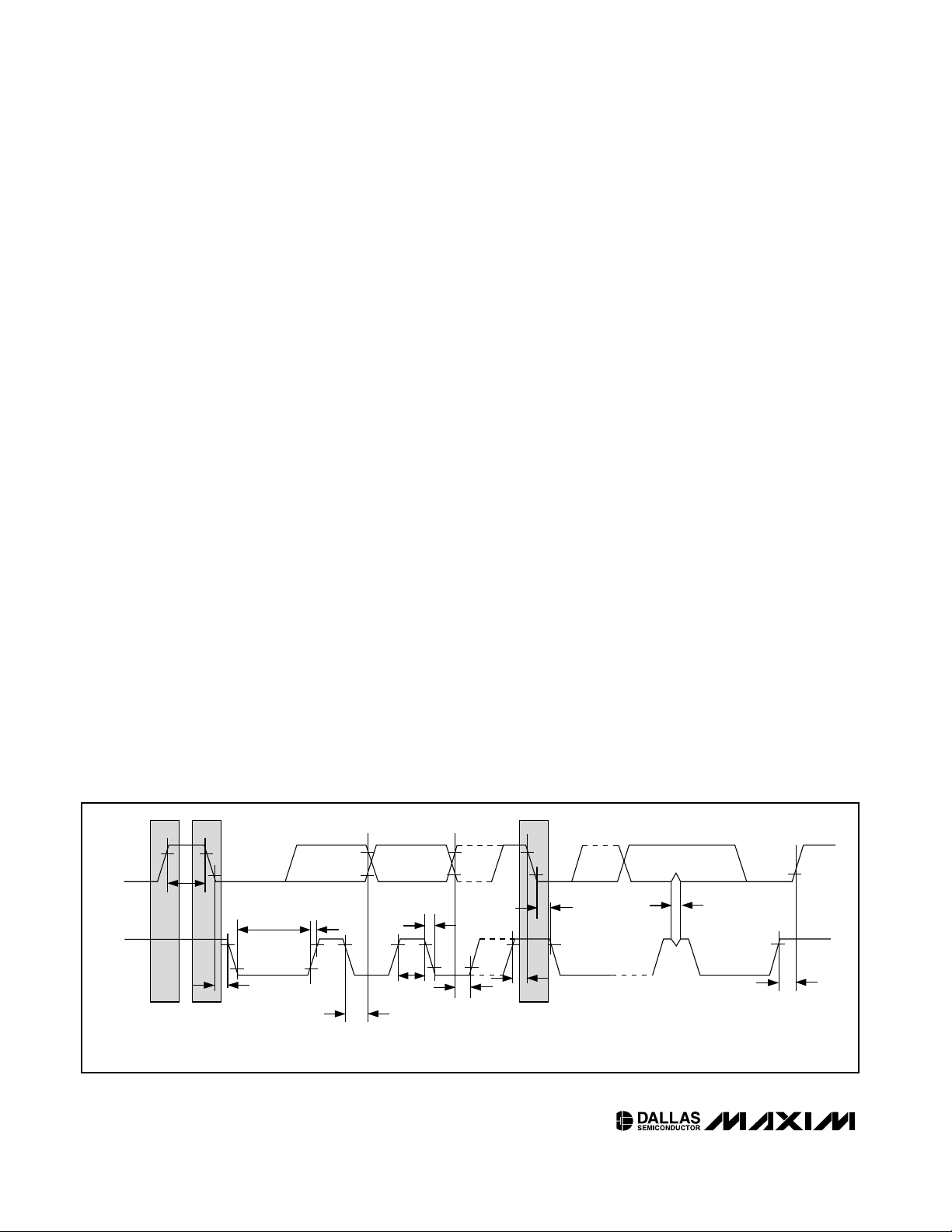
Start condition: A start condition is generated by the
master to initiate a new data transfer with a slave.
Transitioning SDA from high to low while SCL remains
high generates a start condition. See the timing diagram for applicable timing.
Stop condition: A stop condition is generated by the
master to end a data transfer with a slave. Transitioning
SDA from low to high while SCL remains high generates a stop condition. See the timing diagram for
applicable timing.
Repeated start condition: The master can use a
repeated start condition at the end of one data transfer
to indicate that it will immediately initiate a new data
transfer following the current one. Repeated starts are
commonly used during read operations to identify a
specific memory address to begin a data transfer. A
repeated start condition is issued identically to a normal start condition. See the timing diagram for applicable timing.
Bit write: Transitions of SDA must occur during the low
state of SCL. The data on SDA must remain valid and
unchanged during the entire high pulse of SCL plus the
SDA
SCL
t
HD:STA
t
LOW
t
HIGH
t
R
t
F
t
BUF
t
HD:DAT
t
SU:DAT
REPEATED
START
t
SU:STA
t
HD:STA
t
SU:STO
t
SP
STOP
NOTE: TIMING IS REFERENCED TO V
IL(MAX)
AND V
IH(MIN)
.
START
Figure 3. I2C Timing Diagram
TABLE 2 (TEMP LUT FOR POT 1)
Bytes 80h–C7h
POT1 <R/W><NV><00h>The unsigned base value for POT1.
TABLE 3 (TEMP LUT FOR POT 2)
Bytes 80h–C7h
POT2 <R/W><NV><00h>The unsigned base value for POT2.
TABLE 4 (DRAIN LUT FOR POT 1)
Bytes 80h–B8h
POT1 Off <R/W><NV><00h>The signed 2’s complement offset value for POT1.
TABLE 5 (DRAIN LUT FOR POT 2)
Bytes 80h–B8h
POT2 Off <R/W><NV><00h>The signed 2’s complement offset value for POT2.
Page 25
DS1870
LDMOS RF Power-Amplifier Bias
Controller
____________________________________________________________________ 25
setup and hold time requirements (Figure 3). Data is
shifted into the device during the rising edge of the SCL.
Bit read: At the end a write operation, the master must
release the SDA bus line for the proper amount of setup
time (Figure 3) before the next rising edge of SCL during a bit read. The device shifts out each bit of data on
SDA at the falling edge of the previous SCL pulse and
the data bit is valid at the rising edge of the current
SCL pulse. Remember that the master generates all
SCL clock pulses, including when it is reading bits from
the slave.
Acknowledgement (ACK and NACK): An acknowledgement (ACK) or not acknowledge (NACK) is always
the 9th bit transmitted during a byte transfer. The
device receiving data (the master during a read or the
slave during a write operation) performs an ACK by
transmitting a zero during the 9th bit. A device performs a NACK by transmitting a one during the 9th bit.
Timing (Figure 3) for the ACK and NACK is identical to
all other bit writes. An ACK is the acknowledgment that
the device is properly receiving data. A NACK is used
to terminate a read sequence or as an indication that
the device is not receiving data.
Byte write: A byte write consists of 8 bits of information
transferred from the master to the slave (most significant bit first) plus a 1-bit acknowledgement from the
slave to the master. The 8 bits transmitted by the master are done according to the bit write definition and the
acknowledgement is read using the bit read definition.
Byte read: A byte read is an 8-bit information transfer
from the slave to the master plus a 1-bit ACK or NACK
from the master to the slave. The 8 bits of information
that are transferred (most significant bit first) from the
slave to the master are read by the master using the bit
read definition above, and the master transmits an ACK
using the bit write definition to receive additional data
bytes. The master must NACK the last byte read to terminated communication so the slave will return control
of SDA to the master.
Slave address byte: Each slave on the I2C bus
responds to a slave addressing byte sent immediately
following a start condition. The slave address byte
(Figure 4) contains the slave address in the most significant 7 bits and the R/W bit in the least significant bit.
The DS1870’s slave address is 1010A2A1A0 (binary),
where A2, A1, and A0are the values of the address
pins. The address pins allow the device to respond to
one of eight possible slave addresses. By writing the
correct slave address with R/W = 0, the master indicates it will write data to the slave. If R/W = 1, the master will read data from the slave. If an incorrect slave
address is written, the DS1870 assumes the master is
communicating with another I2C device and ignores the
communications until the next start condition is sent.
Memory address: During an I2C write operation, the
master must transmit a memory address to identify the
memory location where the slave is to store the data.
The memory address is always the second byte transmitted during a write operation following the slave
address byte.
I2C Communication
Writing a single byte to a slave: The master must
generate a start condition, write the slave address byte
(R/W = 0), write the memory address, write the byte of
data, and generate a stop condition. Remember the
master must read the slave’s acknowledgement during
all byte write operations.
Writing multiple bytes to a slave: To write multiple
bytes to a slave, the master generates a start condition,
writes the slave address byte (R/W = 0), writes the
memory address, writes up to 8 data bytes, and generates a stop condition.
The DS1870 writes 1 to 8 bytes (1 page or row) with a
single write transaction. This is internally controlled by
an address counter that allows data to be written to
consecutive addresses without transmitting a memory
address before each data byte is sent. The address
counter limits the write to one 8-byte page (one row of
the memory map). Attempts to write to additional pages
of memory without sending a stop condition between
pages results in the address counter wrapping around
to the beginning of the present row.
Example: A 3-byte write starts at address 06h and
writes three data bytes (11h, 22h, and 33h) to three
“consecutive” addresses. The result is that addresses
06h and 07h would contain 11h and 22h, respectively,
and the third data byte, 33h, would be written to
address 00h.
To prevent address wrapping from occurring, the master must send a stop condition at the end of the page,
then wait for the bus-free or EEPROM-write time to
elapse. Then the master can generate a new start con-
1 010
A
2A1A0
7-BIT SLAVE ADDRESS
MOST
SIGNIFICANT BIT
DETERMINES
READ OR WRITE
A
2
, A1, AND A
0
PIN VALUES
R/W
Figure 4. Slave Address Byte
Page 26

DS1870
LDMOS RF Power-Amplifier Bias
Controller
26 ____________________________________________________________________
dition, and write the slave address byte (R/W = 0) and
the first memory address of the next memory row
before continuing to write data.
Acknowledge polling: Any time an EEPROM page is
written, the DS1870 requires the EEPROM write time
(tW) after the stop condition to write the contents of the
page to EEPROM. During the EEPROM write time, the
DS1870 will not acknowledge its slave address
because it is busy. It is possible to take advantage of
that phenomenon by repeatedly addressing the
DS1870, which allows the next page to be written as
soon as the DS1870 is ready to receive the data. The
alternative to acknowledge polling is to wait for maximum period of tWto elapse before attempting to write
again to the DS1870.
EEPROM write cycles: When EEPROM writes occur,
the DS1870 writes the whole EEPROM memory page,
even if only a single byte on the page was modified.
Writes that do not modify all 8 bytes on the page are
allowed and do not corrupt the remaining bytes of
memory on the same page. Because the whole page is
written, bytes on the page that were not modified during the transaction are still subject to a write cycle. This
can result in a whole page being worn out over time by
writing a single byte repeatedly. Writing a page one
byte at a time wears the EEPROM out eight times faster
than writing the entire page at once. The DS1870’s
EEPROM write cycles are specified in the Nonvolatile
Memory Characteristics table. The specification shown
is at the worst-case temperature. It can handle approximately 10x that many writes at room temperature.
Writing to SRAM-shadowed EEPROM memory with SEE
= 1 does not count as an EEPROM write cycle when
evaluating the EEPROM’s estimated lifetime.
Reading a single byte from a slave: Unlike the write
operation that uses the memory address byte to define
where the data is to be written, the read operation occurs
at the present value of the memory address counter. To
read a single byte from the slave, the master generates a
start condition, writes the slave address byte with
R/W = 1, reads the data byte with a NACK to indicate the
end of the transfer, and generates a stop condition.
Manipulating the address counter for reads: A dummy
write cycle can be used to force the address counter to
a particular value. To do this, the master generates a
start condition, writes the slave address byte (R/W = 0),
writes the memory address where it desires to read, generates a repeated start condition, writes the slave
address byte (R/W = 1), reads data with ACK or NACK
as applicable, and generates a stop condition.
S
P
Sr
A
N
START
8 BITS ADDRESS OR DATA
REPEATED
START
STOP
ACK
NOT
ACK
WHITE BOXES INDICATE THE MASTER IS
CONTROLLING SDA
SHADED BOXES INDICATE THE SLAVE IS
CONTROLLING SDA
WRITE A SINGLE BYTE
WRITE UP TO AN 8-BYTE PAGE WITH A SINGLE TRANSACTION
READ A SINGLE BYTE WITH A DUMMY WRITE CYCLE TO MOVE THE ADDRESS COUNTER
READ MULTIPLE BYTES WITH A DUMMY WRITE CYCLE TO MOVE THE ADDRESS COUNTER
COMMUNICATIONS KEY
S
XX XX XX XX
1010 A00
A
MEMORY ADDRESS
A
DATA
A P
S
1010 0
A
MEMORY ADDRESS
A
DATA
A
DATA
A P
S 1010 0 A
MEMORY ADDRESS
A Sr
10 1 0 A01 A DATA N P
S 1010 0 A MEMORY ADDRESS A Sr 10 1 0 1 A DATA A
DATA
A
DATA
A DATA N P
NOTES:
1) ALL BYTES ARE SENT MOST SIGNIFICANT BIT FIRST.
2) THE FIRST BYTE SENT AFTER A START
CONDITION IS ALWAYS THE SLAVE ADDRESS,
FOLLOWED BY THE READ/WRITE BIT.
A1A
2
A0A1A
2
A0A1A
2
A0A1A
2
A1A
2
A0A1A
2
Figure 5. I2C Communications Examples
Page 27

DS1870
LDMOS RF Power-Amplifier Bias
Controller
____________________________________________________________________ 27
See Figure 5 for a read example using the repeated
start condition to specify the starting memory location.
Reading multiple bytes from a slave: The read operation can be used to read multiple bytes with a single
transfer. When reading bytes from the slave, the master
simply ACKs the data byte if it desires to read another
byte before terminating the transaction. After the master
reads the last byte it NACKs to indicate the end of the
transfer and generates a stop condition. This can be
done with or without modifying the address counter’s
location before the read cycle. The DS1870’s address
counter does not wrap on page boundaries during read
operations, but the counter will roll from its upper most
memory address FFh to 00h if the last memory location
is read during the read transaction.
Application Information
Power-Supply Decoupling
To achieve best results, it is recommended that the power
supply is decoupled with a 0.01µF or a 0.1µF capacitor.
Use high-quality, ceramic, surface-mount capacitors, and
mount the capacitors as close as possible to the VCCand
GND pins to minimize lead inductance.
SDA
SCL
A2
A1
A0
FAULT
V
CC
GND
5V
5V REFERENCE
R
POT1
R
POT2
R
S2
R
S1
49.9kΩ
4.22kΩ
RF
POWER
AMP
RF
IN
RF
OUT
W
1
L
1
W
2
H
COM
L
2
N.C. N.C.
N.C.
N.C.
4.7kΩ
3 PLACES
28V
I
D1
I
D2
V
D
FACTORY-CALIBRATED 13-BIT ADC
(CUSTOMER ADJUSTABLE FULL-
SCALE AND OFFSET VALUES)
NOTES:
1) IN THIS CONFIGURATION, THE VOLTAGE RANGE OF W
1
AND W2 IS
3V-5V. THIS RANGE CAN BE EXTENDED USING EXTERNAL RESISTORS.
2) ONE MAX6156B CAN BE USED WITH MULTIPLE DS1870s.
DS1870
MAX6165B
Typical Operating Circuit
Page 28

DS1870
LDMOS RF Power-Amplifier Bias
Controller
Maxim cannot assume responsibility for use of any circuitry other than circuitry entirely embodied in a Maxim product. No circuit patent licenses are
implied. Maxim reserves the right to change the circuitry and specifications without notice at any time.
28 ____________________Maxim Integrated Products, 120 San Gabriel Drive, Sunnyvale, CA 94086 408-737-7600
© 2004 Maxim Integrated Products Printed USA is a registered trademark of Maxim Integrated Products.
DALLAS is a registered trademark of Dallas Semiconductor Corporation.
SDA and SCL Pullup Resistors
SDA is an open-collector output on the DS1870 that
requires a pullup resistor to realize high logic levels. A
master using either an open-collector output with a
pullup resistor or a push-pull output driver can be used
for SCL. Pullup resistor values should be chosen to
ensure that the rise and fall times listed in the AC electrical characteristics are within specification.
Advanced Application
A circuit showing the implementaion of current sensing
using the DS1870 is shown under “Advanced
Application”.
SDA
SCL
A2
A1
A0
FAULT
V
CC
GND
5V
5V REFERENCE
R
POT1
49.9k
(1%)
LOW
PASS
FILTER
R
POT2
R
S2
R
S1
4.22k
(1%)
VD
ID1
ID2
RF
POWER
AMP
RF
IN
RF
OUT
W
1
L
1
W
2
H
COM
L
2
N.C. N.C.
4.7kΩ
3 PLACES
NOTES:
1) IN THIS CONFIGURATION, THE VOLTAGE RANGE OF W
1
AND W2 IS
3V-5V. THIS RANGE CAN BE EXTENDED USING EXTERNAL RESISTORS.
2) ONE MAX6156B CAN BE USED WITH MULTIPLE DS1870s.
DS1870
MAX6165B
MAX4080
LOW
PASS
FILTER
MAX4080
28V
Advanced Application with Current Sense
Chip Information
TRANSISTOR COUNT: 52,353
SUBSTRATE CONNECTED TO GROUND
Package Information
For the latest package outline information, go to
www.maxim-ic.com/DallasPackInfo.
 Loading...