Page 1

www.dalsemi.com
DS1867
Dual Digital Potentiometer with EEPROM
FEATURES
Nonvolatile version of the popular DS1267
Low power consumption, quiet, pumpless
design
Operates from single 5V or ±5V supplies
Two digitally controlled, 256-position
potentiometers
Wiper position is maintained in the absence of
power
Serial port provides means for setting and
reading both potentiometers
Resistors can be connected in series to
provide increased total resistance
16-pin SOIC and 20-pin TSSOP for surface
mount applications
Standard resistance values:
- DS1867-10 ~ 10 kΩ
- DS1867-50 ~ 50 kΩ
- DS1867-100 ~ 100 kΩ
Operating Temperature Range:
- Industrial: -40°C to +85°C
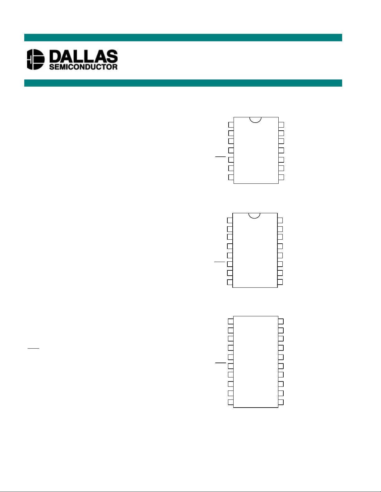
PIN ASSIGNMENT
V
114V
B
H1 2 13 S
L1 3 12 WO
W1 4 11 HO
RST 5 10 LO
CLK 6 9 C
GND 7 8 DQ
14-Pin DIP (300-mil)
See Mech. Drawings Section
V
116V
B
NC 2 15 NC
H1 3 14 S
L1 4 13 WO
W1 5 12 HO
RST 6 11 LO
CLK 7 10 C
GND 8 9 DQ
CC
OUT
OUT
CC
OUT
OUT
PIN DESCRIPTION
L0, L1 - Low End of Resistor
H0, H1 - High End of Resistor
W1, W2 - Wiper End of Resistor
V
B
S
OUT
RST
DQ - Serial Port Data Input
CLK - Serial Port Clock Input
C
OUT
V
CC
GND - Ground
NC - No Internal Connection
DNC - Do Not Connect
-Substrate Bias
- Wiper for Stacked Configuration
- Serial Port Reset Input
- Cascade Serial Port Output
- +5-Volt Supply Input
16-Pin SOIC (300-mil)
See Mech. Drawings Section
V
1 20 V
B
NC 2 19 DNC
H1 3 18 DNC
L1 4 17 S
W1 5 16 WO
RST 6 15 HO
CLK 7 14 LO
DNC 8 13 C
DNC 9 12 DNC
GND 10 11 DQ
20-Pin TSSOP (173-mil)
See Mech. Drawings Section
CC
OUT
OUT
1 of 14 102199
Page 2

DS1867
DESCRIPTION
The DS1867 Dual Digital Potentiometer with EEPROM is the nonvolatile version of the popular DS1267
Dual Digital Potentiometer. The DS1867 consists of two digitally controlled potentiometers having 256position wiper settings. Wiper position is maintained in the absence of power through the use of
EEPROM memory cell arrays. Communication and control of the device are accomplished over a 3-wire
serial port which allows reads and writes of the wiper position. Both potentiometers can be stacked for
increased total resistance with the same resolution. For multiple-device, single-processor environments,
the DS1867 can be cascaded for control over a single 3-wire bus. The DS1867 is offered in three standard
resistance values.
OPERATION
The DS1867 contains two 256-position potentiometers whose wiper positions are set by an 8-bit value.
These two 8-bit values are written to a 17-bit I/O shift register which is used to store wiper position and
the stack select bit when the device is powered. An additional memory area, the shadow memory, stores
the 17-bit I/O shift register during a power-down sequence which provides for wiper nonvolatility. A
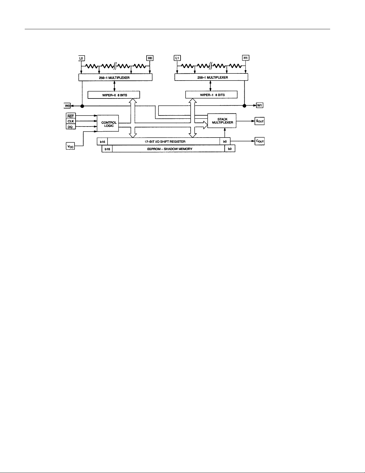
block diagram of the DS1867 is presented in Figure 1.
Communication and control of the DS1867 is accomplished through a 3-wire serial port interface that
drives an internal control logic unit. The 3-wire serial interface consists of the three input signals: RST ,
CLK, and DQ.
The RST control signal is used to enable 3-wire serial port operation of the device. The RST signal is an
active high input and is required to begin any communication to the DS1867. The CLK signal input is
used to provide timing synchronization for data input and output. The DQ signal line is used to transmit
potentiometer wiper settings and the stack select bit configuration to the 17-bit I/O shift register of the
DS1867.
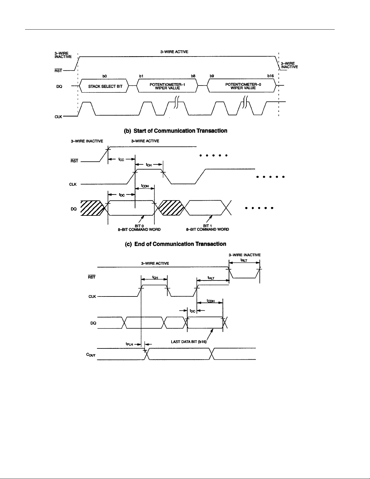
Figure 2(a) presents the 3-wire serial port protocol. As shown, the 3-wire port is inactive when the RST
signal input is low. Communication with the DS1867 requires the transition of the RST input from a low
state to a high state. Once the 3-wire port has been activated, data is latched into the part on the low to
high transition of the CLK signal input. Three-wire serial timing requirements are provided in the t iming
diagrams of Figure 2(b) and (c).
Data written to the DS1867 over the 3-wire serial interface is stored in the 17-bit I/O shift register (see
Figure 3). The 17-bit I/O shift register contains both 8-bit potentiometer wiper position values and the
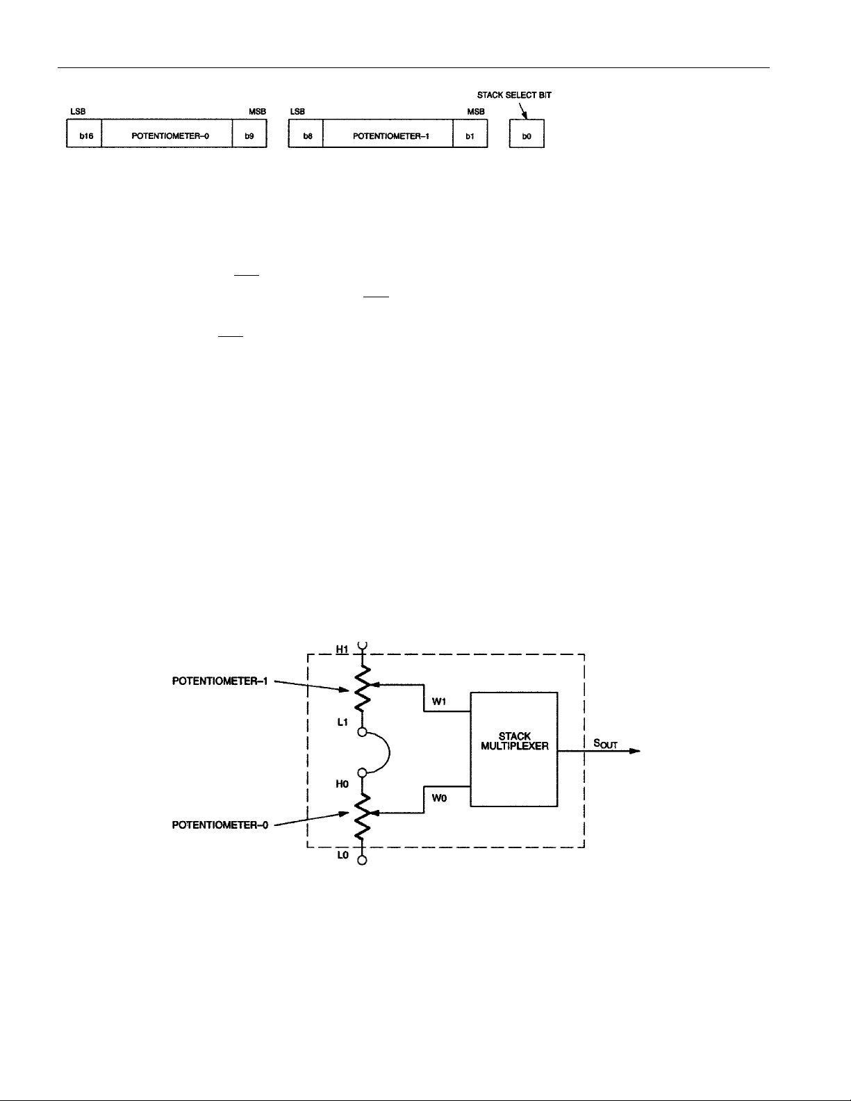
stack select bit. The composition of the I/O shift register is presented in Figure 3. Bit 0 of the I/O shift
register contains the stack select bit. This bit will be discussed in the section entitled Stacked
Configuration. Bits 1 through 8 of the I/O shift register contain the potentiometer-1 wiper position value.
Bit 1 will contain the MSB of the wiper setting for potentiometer-1 and bit 8 the LSB for the wiper
setting. Bits 9 through 16 of the I/O shift register contain the value of the potentiometer-0 wiper position
with the MSB for the wiper position occupying bit 9 and the LSB bit 16.
2 of 14 102199
Page 3

DS1867 BLOCK DIAGRAM Figure 1
DS1867
3 of 14 102199
Page 4

TIMING DIAGFRAMS Figure 2
(a) 3-Wire Serial Interface General Overview
DS1867
4 of 14 102199
Page 5

DS1867
I/O SHIFT REGISTER Figure 3
17-BIT I/O SHIFT REGISTER
Transmission of data always begins with the stack select bit followed by the potentiometer-1 wiper
position value and lastly the potentiometer-0 wiper position value (see Figure 2(a)).
When wiper position data is to be written to the DS1867, 17-bits (or some integer multiple) of data should
always be transmitt ed. Transactions which do not send a complete 17-bits (or multiple) will leave the
register incomplete and possibly an error in desired wiper position. After a communication transaction
has been completed the RST signal input should be taken to a low state to prevent any inadvertent
changes to the device shift register. Once RST has reached a low state, the contents of the I/O shift
register are loaded into the respective multiplexers for setting wiper position. A new wiper position will
only engage pending a RST transition to the low state. The wiper position for the high-end terminals H0
and H1 will have data values FF (hex), while the low-end terminals will have data values 00 (hex).
STACKED CONFIGURATION
The potentiometers of the DS1867 can be connected in series as shown in Figure 4. This is referred to as
the stacked configuration and allows the user to double the total end-to-end resistance of the part. The
resolution of the combined pot entiometers will remain the same as a single potentiometer but with a total
of 512 wiper positions available. Device resolution is defined as R
R
is equal to the device resistance value. The wiper output for the combined stacked potentiometer will
TOT
be taken at the S
potentiometer-1 (W1). The potentiometer wiper selected at the S
pin, which is the multiplexed output of the wiper of potentiometer-0 (W0) or
out
out
the stack select bit (bit-0) of the 17-bit I/O shift register. If the stack select bit has value 0, the multiplexed
output, S
output, S
, will be that of the potentiometer-0 wiper. If the stack select bit has value 1, the multiplexed
out
, will be that of the potentiometer-1 wiper.
out
/256 (per potentiometer); where
TOT
output is governed by the setting of
STACKED CONFIGURATION Figure 4
CASCADE OPERATION
A feature of the DS1867 is the ability to control multiple devices from a single processor. Multiple
DS1867s can be linked or daisy-chained as shown in Figure 5. As a data bit is entered into the I/O shift
register of the DS1867 it will appear at the C
output after a maximum delay of 70 nanoseconds.
out
5 of 14 102199
Page 6

DS1867
The C
output of the DS1867 can be used to drive the DQ input of another DS1867. When connecting
out
multiple devices, the total number of bits sent is always 17 times the number of DS1867s in the daisy
chain.
An optional feedback resistor can be placed between the C
terminal of the last device and the DQ input
out
of the first DS1867, thus allowing the controlling processor to read, as well as, write data or circularly
clock data through the daisy chain. The value of the feedback or isolation resistor should be in the range
from 2 to 10 kohms.
When reading data via the C
device. When RST is driven high, bit 17 is present on the C
pin and isolation resistor, the DQ line is left floating by the reading
OUT
pin, which is fed back to the input DQ pin
OUT
through the isolation resistor. When the CLK input transitions low to high, bit 17 is loaded into the first
position of the I/O shift register and bit 16 becomes present on C
and DQ of the next device. After 17
OUT
bits (or 17 times the number of DS1867s in the daisy chain), the data has shifted completely around and
back to its original position. When RST transitions to the low state to end data transfer, the value (the
same as before the read occurred) is loaded into the wiper-0, wiper-1, and stack select bit I/O register.
CASCADING MULTIPLE DEVICES Figure 5
NONVOLATILE WIPER SETTINGS
The DS1867 maintains the position of the wiper in the absence of power. This feature is provided through
the use of EEPROM type memory cell arrays. During normal operation, the position of the wiper is
determined by the device multiplexers and stored in the shadow memory (EEPROM). The manner in
which an update occurs has been optimized for reliability, durability, and performance. Additionally, the
update operation is totally transparent to the user.
When power is applied to the DS1867, wiper settings will be the last recorded in the EEPROM memory
cells or shadow memory before the last power-down. Changes to the EEPROM memory cells occur
during a predefined power-down sequence. If the DS1867 detects a voltage transition to 4.5 volts or less,
on the power supply input, the part initiates an automatic wiper storage sequence. This storage sequence
will save in EEPROM memory the contents of the I/O shift register before a total power-shutdown;
provided specific power-down timing requirements are met. The minimum total power-down time is
specified at 4 milliseconds. Power-down timing requirements on VCC are shown in Figure 6.
The EEPROM memory cells are specified to accept greater than 25,000 writes before a wear-out
condition. If the EEPROM memory cells do reach a wear-out condition, the DS1867 will still function
properly while power is applied. A minimum time of 4 ms between 4.5V and 3V is required to perform
the proper position storage of the wiper.
6 of 14 102199
Page 7

DS1867
POWER-DOWN EEPROM TIMING REQUIREMENTS Figure 6
TYPICAL APPLICATION CONFIGURATIONS
Figures 7 and 8 show two typical application configurations for the DS1867. By connecting the wiper
terminal of the part to a high impedance load, the effects of the wiper resistance is minimized, since the
wiper resistance can vary from 400 to 1000 ohms depending on wiper voltage. Figure 7 presents the
device connected in an inverting variable gain amplifier. The gain of the circuit on Figure 7 is given by
the following equation:
Av = -n/(255-n); where n = 0 to 255
Figure 8 shows the device operating in a fixed gain attenuator where the potentiometer is used to
attenuate an incoming signal. Note the resistance R1 is chosen to be much greater than the wiper
resistance to minimize its effect on circuit gain.
INVERTING VARIABLE GAIN AMPLIFIER Figure 7
7 of 14 102199
Page 8

DS1867
FIXED GAIN ATTENUATOR Figure 8
ABSOLUTE AND RELATIVE LINEARITY
Absolute linearity is defined as the difference between the actual measured output voltage and the
expected output voltage. Figure 9 presents the test circuit used to measure absolute linearity. Absolute
linearity is given in terms of a minimum increment or expected output when the wiper position is moved
one position. In the case of the test circuit, a minimum increment (MI) would equal 10/512volts. The
equation for absolute linearity is given in equation (1).
Eq: (1) Absolute Linearity
AL = {Vo(actual)- Vo(expected)}/MI
Relative linearity is a measure of error between two adjacent wiper position points and is given in terms
of MI by equation (2).
Eq: (2) Relative Linearity
RL = {Vo(n+1) - Vo(n)}/MI
Figure 10 is a plot of absolute linearity and relative linearity versus wiper position for the DS1867 at
25°C. The specification for absolute linearity of the DS1867 is ±0.75 MI typical. The specification for
relative linearity of the DS1867 is ±0.30 MI typical.
LINEARITY MEASUREMENT CONFIGURATION Figure 9
8 of 14 102199
Page 9

DS1867
9 of 14 102199
Page 10

DS1867
ABSOLUTE MAXIMUM RATINGS*
Voltage on Any Pin Relative to Ground (VB=GND) -1.0V to +5.5V
Voltage on Resistor Pins when VB=-5.5V -5.5V to +5.5V
Operating Temperature -40° to +85°C
Storage Temperature -55°C to +125°C
Soldering Temperature 260°C for 10 seconds
* This is a stress rating only and functional operation of the device at these or any other conditions above
those indicated in the operation sections of this specification is not implied. Exposure to absolute
maximum rating conditions for extended periods of time may affect reliability.
RECOMMENDED DC OPERATING CONDITIONS (-40°C to +85°C)
PARAMETER SYMBOL MIN TYP MAX UNITS NOTES
Supply Voltage V
Input Logic 1 V
Input Logic 0 V
Substrate Bias V
CC
IH
IL
B
Resistor Inputs L,H,W V
4.5 5.5 V
2.0 VCC+0.5 V 1
-0.5 +0.8 V 1
-5.5 GND V
B
VCC+0.5 V 2
DC ELECTRICAL CHARACTERISTICS (-40°C to +85°C; VCC=5V ± 10%)
PARAMETER SYMBOL MIN TYP MAX UNITS NOTES
Supply Current I
Input Leakage I
Wiper Resistance R
Wiper Current I
Logic 1 Output @2.4Volts I
Logic 0 Output @0.4Volts I
CC
LI
W
OH
OL
-1 +1 µA
W
-1.0 mA 8
4mA8
250 900 µA
400 1000
Ω
1mA
Standby Current I
Power-Down Time t
STBY
PU
t
PU1
4
2.5
250 µA
ms
ms
Power Trip Point 3.9 4.2 4.5 V
Recovery Time t
REC
2 5 10 ms 11,14
10 of 14 102199
9
10
Page 11

DS1867
ANALOG RESISTOR CHARACTERISTICS (-40°C to +85°C;VCC= 5V ± 10%)
PARAMETER SYMBOL MIN TYP MAX UNITS NOTES
End-to-End Resistor Tolerance -20 +20 % 17
Absolute Linearity ±0.75
Relative Linearit y ±0.30
-3 dB Cutoff Frequency f
CUTOFF
LSB
LSB
Hz 7
4
5
Noise Figure 120 dB/(Hz)1/2
Temperature Coefficient 750 ppm/°C
CAPACITANCE (TA = 25°C)
PARAMETER SYMBOL MIN TYP MAX UNITS NOTES
Input Capacitance C
Output Capacitance C
IN
OUT
5pF 3
7pF3
AC ELECTRICAL CHARACTERISTICS (-40°C to +85°C; VCC= 5V ± 10%)
PARAMETER SYMBOL MIN TYP MAX UNITS NOTES
CLK Frequency f
Width of CLK Pulse t
CLK
CH
DC 10 MHz 15
50 ns 15
Data Setup Time t
Data Hold Time t
Propagation Delay Time
DC
CDH
t
PLH
30 ns 15
10 ns 15
70 ns 13,15
Low to High Level
Clock to Output
Propagation Delay Time
t
PHL
70 ns 13,15
High to Low Level
Clock to Output
High to Clock Input High
RST
Low to Clock Input High
RST
CLK Rise Time t
Inactive
RST
t
t
HLT
t
RLT
CC
CR
50 ns 15
50 ns 15
50 ns 15
200 ns 15
NONVOLATILE MEMORY CHARACTERISTICS
(-40°C to +85°C; V
PARAMETER SYMBOL MIN TYP MAX UNITS NOTES
= 5V ± 10%)
CC
Writes 25000 16
11 of 14 102199
Page 12

DS1867
NOTES:
1. All voltages are referenced to ground.
2. Resistor inputs cannot exceed the substrate bias voltage, VB, in the negative direction.
3. Capacitance values apply at 25°C.
4. Absolute linearity is used to determine wiper voltage versus expected voltage as determined by wiper
position. Test limits for absolute linearity are ±1.6 LSB.
5. Relative linearity is used to determine the change in voltage between successive tap positions. Test
limits for relative linearity are ±0.5 LSB.
6. Typical values are for tA=25°C and nominal supply voltage.
7. -3 dB cutoff frequency characteristics for the DS1867 depend on potentiometer total resistance:
DS1867-010; 1 MHz, DS1867-050; 200 kHz, DS1867-100; 100 kHz.
8. C
is active regardless of the state of
OUT
RST
.
9. Power-down time is specified at a minimum of 4 ms. It is the time required for the DS1867 to
guarantee wiper position storage as VCCmoves from 4.5V to 3.0V.
10. This is the time from power trip-point min (3.9V) to 3.0V to guarantee wiper storage.
11. t
is the time required before the DS1867 stored wiper position becomes valid on power-up.
REC
12. Power trip points reference required voltage necessary for DS1867 to restore the stored wiper position
setting.
13. See Figure 11.
14. During power-up the wiper position will be set at 80H.
15. See Figure 2.
16. A device write is specified as being a controlled power-down providing enough time to complete an
EEPROM write. It is also defined as a complete bit change from one value to another, i.e., 0 to 1.
Power-downs which do not change the wiper value can be expected have 200,000-write durability.
17. Valid at 25°C only.
12 of 14 102199
Page 13

ABSOLUTE AND RELATIVE LINEARITY Figure 10
Abso lute and Relative Linearity
(Normalized to 1 LSB)
DS1867
DIGITAL OUTPUT LOAD SCHEMATIC Figure 11
13 of 14 102199
Page 14

TYPICAL SUPPLY CURRENT VS. SERIAL CLOCK RATE Figure 12
DS1867
Serial Clock Rate (bits/second)
14 of 14 102199
 Loading...