

Page 1
www.dalsemi.com
DS1866
Log Trimmer Potentiometer
FEATURES
Single 8-position Log Trimmer Potentiometer
5-dB/step
Operates from 2.7V to 5.5V supplies
Parallel interface control: P0, P1, P2
Standard Resistance Value: 10 kΩ
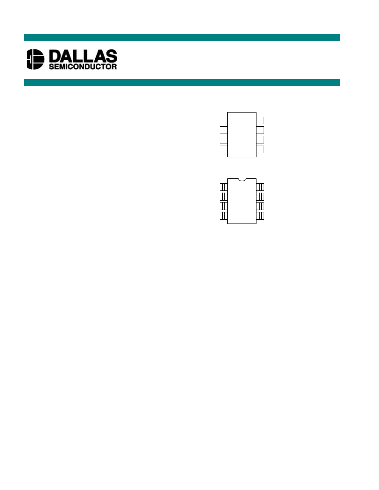
8-pin DIPs; 8-pin (150) SOICs
Operating Temperature Range:
- Industrial: -40°C to +85°C
PIN ASSIGNMENT
1
P0
P1
2
H
3
GND
See Mech. Drawings Section
GND
See Mech. Drawings Section
4
8-Pin DIP (300-mil)
1
P0
2
P1
3
H
4
8-Pin SOIC (150-mil)
8
V
CC
7
P2
6
L
5
W
V
8
CC
P2
7
L
6
W
5
PIN DESCRIPTION
H - High End of Resistor
L - Low End of Resistor
W - Wiper Terminal
V
CC
P0 - Position Select - Bit 0
P1 - Position Select - Bit 1
P2 - Position Select - Bit 2
GND - Ground
- 3V or 5V Power Supply Input
DESCRIPTION
The DS1866 Log Trimmer Potentiometer is a single volatile digital potentiometer having eight positions
with a 5-dB resolution per st ep. The device provides an ideal method for low-cost trimming or volume
control using a CPU or manual control input. The device’s wiper position is set to one of eight positions
by a 3-terminal parallel port. The value of the wiper position is determined by the P0, P1, and P2 port
pins.
The DS1866 is available as a 10k potentiometer and is available in an industrial temperature grade.
Additionally, the DS1866 will operate from 3V or 5V supplies and is ideal for portable applications
requiring low standby current. Two packaging options are available and include the 8-pin (300-mil) DIP,
8-pin (150-mil) SOIC.
1 of 5 102199
Page 2

DS1866
OPERATION
The DS1866 is a single volatile potentiometer. The device has a total of eight positions providing a
resolution of 5 dB per step and giving a total attenuation range of 0 dB to -35 dB. These tap points are
accessible to the W-terminal whose position is controlled via a 3-terminal parallel port consisting of input
signals P0, P1, and P2. A block diagram of the DS1866 is shown in Figure 1.
Wiper position setting of the DS1866 is determined by the states of the P0, P1, and P2 input terminals.
Table 1 below outlines position setting versus value of the parallel port inputs. A Position-0 setting places
the wiper position at the L-terminal of the potentiometer and provides 35 dB of attenuation. As wiper
position increases, attenuation decreases with Position-7 giving 0 dB of attenuation.
On power-up, the wiper position of the DS1866 will be set to the P0, P1, and P2 values.
P2 P1 P0
(binary)
000 0 35 dB
001 1 30 dB
010 2 25 dB
011 3 20 dB
100 4 15 dB
101 5 10 dB
110 6 5 dB
111 7 0 dB
Wiper
Position
Attenuation
(dB)
PIN DESCRIPTIONS
VCC - Power Supply Terminal. The DS1866 will support supply voltages ranging from +2.7 to +5.5
volts.
GND - Ground Terminal.
H - High-end Resistor. This is the high-end terminal of the potentiometer. It is not required that this
terminal be connected to a potential greater than the L-terminal. Maximum voltage on the H-terminal can
not exceed the power supply voltage, VCC, or go below ground.
L - Low-end Resistor. This is the low-end terminal of the potentiometer. It is not required that this
terminal be connected to a potential less than the H-terminal. Maximum voltage on the L-terminal can not
exceed the power-supply voltage, VCC, or go below ground.
W - Wiper of the Potentiometer. This pin is the wiper terminal of the potentiometer. Its position on the
resistor array is controlled by the 3-terminal parallel port. Maximum voltage on the W-terminal can not
exceed the power supply voltage, VCC, or go below ground.
P0 - Bit 0. P0 is the bit 0 data input to the parallel port.
P1 - Bit 1. P1 is the bit 1 data input to the parallel port.
P2 - Bit 2. P2 is the bit 2 data input to the parallel port.
2 of 5 102199
Page 3

DS1866
One Time Programmability (OTP). The DS1866 can be easily used as an OTP device. This can be
accomplished by terminating the P0, P1, or P2 to desired logic levels during system manufacturing. On
power up, the value of P0, P1, and P2 will then set the wiper position setting of the DS1866.
DS1866 BLOCK DIAGRAM Figure 1
3 of 5 102199
Page 4

DS1866
ABSOLUTE MAXIMUM RATINGS*
Voltage on Any Pin Relative to Ground -0.5V to +7.0V
Operating Temperature -40°C to +85°C
Storage Temperature -55°C to +125°C
Soldering Temperature 260°C for 10 seconds
* This is a stress rating only and functional operation of the device at these or any other conditions
above those indicated in the operation sections of this specification is not implied. Exposure to
absolut e maximum rating conditions for extended periods of time may affect reliability.
RECOMMENDED DC OPERATING CONDITIONS (-40°C to +85°C)
PARAMETER SYMBOL MIN TYP MAX UNITS NOTES
Supply Voltage V
Input Logic 1 V
Input Logic 0 V
CC
IH
IL
+2.7 5.5 V 1
2.0 VCC +0.5 V 1, 2
-0.5 +0.8
V1, 2
+0.6
Ground GND GND -0.5 GND +0.5
Resistor Inputs L, H, W GND -0.5 VCC +0.5 V 1, 3
DC ELECTRICAL CHARACTERISTICS (-40°C to +85°C; VCC = 2.7V to 5.5V)
PARAMETER SYMBOL MIN TYP MAX UNITS NOTES
Supply Current I
Input Leakage I
Wiper Resistance R
Wiper Current I
Standby Current
I
STBY
3 volts
5 volts
CC
U
W
-1 +1 µA
W
400 1000
10
25 50
400 µA 4
Ω
1mA
µA
µA
5
ANALOG RESISTOR CHARACTERISTICS (-40°C to +85°C; VCC = 2.7V to 5.5V)
PARAMETER SYMBOL MIN TYP MAX UNITS NOTES
End to End Resistor
-20 +20 % 6
Tolerance
Absolute Tolerance -1.0 +1.0 dB 8
Tap-to-Tap -1.0 +1.0 dB 9
-3 dB Cutoff Frequency f
Temperature Coefficient
CUTOFF
1 MHz MHz 10
750 ppm/°C
CAPACITANCE (25°C; VCC = 2.7V to 5.5V)
PARAMETER SYMBOL MIN TYP MAX UNITS NOTES
Input Capacitance C
Output Capacitance C
IN
OUT
5pF11
7pF11
AC ELECTRICAL CHARACTERISTICS (-40°C to +85°C; VCC = 2.7V to 5.5V)
PARAMETER SYMBOL MIN TYP MAX UNITS NOTES
Parallel Port Transition t
PC
4 of 5 102199
500 ns 12
Page 5

NOTES:
1. All voltages are referenced to ground.
DS1866
2. For VCC = 5V ± 10% maximum VIL = +0.8V. For VCC 3.0 ± 10% VIL = +0.6V. For VCC =2.7 volts V
IH
=2.0 volt s minimum.
3. Resistor input voltages cannot go below ground or exceed V
by the amounts as shown in the table.
CC
4. Maximum current specifications are based on the change rate of the parallel port inputs P0, P1, and
P2.
5. Standby current specifications apply when P0, P1, P2 logic inputs are driven within the specified V
IH
or VIL levels.
6. Valid at 25°C only.
7. The end-to-end resistance tolerance of the DS1866 can be expected to shift with temperature.
However, this change will not exceed ±20% of the nominal resistor value of the part.
8. Absolute tolerance is used to compare measured wiper voltage versus expected wiper voltage as
determined by wiper position. The DS1866 is specified to provide an absolute tolerance of ±1.0 dB.
9. Tap-to-tap tolerance is used to determine the change in voltage between successive tap positions. The
DS1866 is specified to provide a tap-to-tap tolerance specification of ±1.0 dB.
10. -3 dB cutoff frequency characteristic for the DS1866 is 1 MHz.
11. Capacitance values apply at 25°C.
12. This specification refers to the time difference between parallel port input changes to stabilize a wiper
transition.
DS1866 ORDERING INFORMATION
ORDERING NUMBER
PACKAGE
DS1866 8L DIP -40°C TO +85°C
DS1866Z 8L SOIC (150-MIL) -40°C TO +85°C
OPERATING
TEMPERATURE
VERSION
10kΩ
10kΩ
5 of 5 102199
 Loading...