

Page 1
General Description
The DS1862 is a closed-loop laser-driver control IC with
built-in digital diagnostics designed for XFP MSA. The
laser control function incorporates average power control (APC) and allows extinction ratio control though a
temperature indexed look-up table (LUT). The DS1862
monitors up to seven analog inputs, including temperature and monitor diode (MD) current, which are used to
regulate the laser bias current and extinction ratio.
Warning and alarm thresholds can be programmed to
generate an interrupt if monitored signals exceed tolerance. Calibration is also provided internally using independent gain and offset scaling registers for each of
the monitored analog signals. Settings such as programmed calibration data are stored in password-protected EEPROM memory. Programming is accomplished
through an I2C*-compatible interface, which can also be
used to access diagnostic functionality.
Applications
Laser Control and Monitoring 10Gbps Optical
Transceiver Modules (XFP)
Laser Control and Monitoring
Digital Diagnostics in Optical Transmission
Features
♦ Implements XFP MSA Requirements for Digital
Diagnostics, Serial ID, and User Memory
♦ I2C-Compatible Serial Interface
♦ Automatic Power Control (APC)
♦ Extinction Ratio Control with Look-Up Table
♦ Seven Monitored Channels for Digital Diagnostics
(Five Basic Plus Two Auxiliary)
♦ Internal Calibration of Monitored Channels
(Temp, V
CC2/3
, Bias Current, Transmitted, and
Received Power)
♦ Programmable Quick-Trip Logic for Turning
Off Laser for Eye Safety
♦ Access to Monitoring and ID Information
♦ Programmable Alarm and Warning Thresholds
♦ Operates from 3.3V or 5V Supply
♦ 25-Pin CSBGA, 5mm x 5mm Package
♦ Internal or External Temperature Sensor
♦ -40°C to +100°C Operating Temperature Range
♦ One 8-Bit Buffered DAC
DS1862
XFP Laser Control and Digital Diagnostic IC
______________________________________________ Maxim Integrated Products 1
CSBGA (5mm x 5mm)
TOP VIEW
1
A
B
C
D
E
2345
Pin Configuration
Rev 0; 2/06
For pricing, delivery, and ordering information, please contact Maxim/Dallas Direct! at
1-888-629-4642, or visit Maxim’s website at www.maxim-ic.com.
+Denotes lead-free package.
Ordering Information
Typical Operating Circuit appears at end of data sheet.
PART TEMP RANGE PIN-PACKAGE
DS1862B
25 CSBGA (5mm x 5mm)
DS1862B+
25 CSBGA (5mm x 5mm)
*Purchase of I2C components from Maxim Integrated Products, Inc., or one of its sublicensed Associated Companies, conveys a
license under the Philips I
2
C Patent Rights to use these components in an I2C system, provided that the system conforms to the I2C
Standard Specification as defined by Philips.
-40°C to +100°C
-40°C to +100°C
Page 2
DS1862
XFP Laser Control and Digital Diagnostic IC
2 _____________________________________________________________________
ABSOLUTE MAXIMUM RATINGS
RECOMMENDED OPERATING CONDITIONS
(V
CC3
= +2.9V to +5.5V, TA= -40°C to +100°C, unless otherwise noted.)
Stresses beyond those listed under “Absolute Maximum Ratings” may cause permanent damage to the device. These are stress ratings only, and functional
operation of the device at these or any other conditions beyond those indicated in the operational sections of the specifications is not implied. Exposure to
absolute maximum rating conditions for extended periods may affect device reliability.
Voltage on Any Open-Drain Pin
Relative to Ground.............................................-0.5V to +6.0V
Voltage on MOD-DSEL, SDA, SCL, FETG, THRSET, TX-D,
AUX1MON, AUX2MON, IBIASMON,
RSSI, BIASSET, MODSET, EN1,
and EN2 ............-0.5V to (V
CC3
+ 0.5V), not to exceed +6.0V
Voltage on SC-RX-LOS, SC-RX-LOL, RX-LOS, SC-TX-LOS,
MOD-NR, EN1,
and EN2 ............-0.5V to (V
CC2
+ 0.5V), not to exceed +6.0V
Operating Temperature Range .........................-40°C to +100°C
EEPROM Programming Temperature Range .........0°C to +70°C
Storage Temperature Range .............................-55°C to +125°C
Soldering Temperature...................See J-STD-020 Specification
PARAMETER
CONDITIONS
UNITS
Main Supply Voltage V
CC3
(Note 1)
V
Secondary Supply Voltage V
CC2
V
CC2
not to exceed V
CC3
(Note 2)
V
High-Level Input Voltage
(SDA, SCL)
V
IH
IIH (max) = 10µA
0.7 x
V
CC3
+
0.5
V
Low-Level Input Voltage
(SDA, SCL)
V
IL
IIL (max) = -10µA
GND -
0.3
0.3 x
V
High-Level Input Voltage
(TX-D, MOD-DESEL,
P-DOWN/RST) (Note 3)
V
IH
IIH (max) = 10µA 2
V
CC3
+
0.3
V
Low-Level Input Voltage
(TX-D, MOD-DESEL,
P-DOWN/RST) (Note 3)
V
IL
IIL (max) = -10µA
V
SYMBOL
MIN TYP MAX
+2.9 +5.5
+1.6 +3.6
V
CC3
V
CC3
-0.3 +0.8
Page 3
DS1862
XFP Laser Control and Digital Diagnostic IC
_____________________________________________________________________ 3
DC ELECTRICAL CHARACTERISTICS
(V
CC3
= +2.9V to +5.5V, V
CC2
= +1.6V to +3.6V, TA= -40°C to +100°C, unless otherwise noted.)
PARAMETER
CONDITIONS
UNITS
Supply Current I
CC3
P-DOWN/RST = 1 3 5 mA
High-Level Output Voltage
(FETG)
V
OH
IOH (max) = -2mA
V
CC3
-
0.5
V
Low-Level Output Voltage
(MOD-NR, INTERRUPT, SDA,
and FETG)
V
OL
IOL (max) = 3mA 0 0.4 V
Resistor (Pullup) R
PU
91215kΩ
I/O Capacitance C
I/O
(Note 4) 10 pF
Leakage Current I
L
-10
µA
Leakage Current (SCL, SDA) I
L
-10
µA
Digital Power-On Reset POD 1.0 2.2 V
Analog Power-On Reset POA 2.0 2.6 V
DC ELECTRICAL CHARACTERISTICS—INTERFACE SIGNALS TO SIGNAL CONDITIONERS
(V
CC2
= +1.6V to +3.6V, V
CC3
= +2.9V to +5.5V, TA= -40°C to +100°C, unless otherwise noted.)
PARAMETER
CONDITIONS
UNITS
High-Level Input Voltage
(SC-RX-LOS, SC-RX-LOL,
and SC-TX-LOS)
V
IH
IIH (max) = 100µA
0.7 x
V
CC2
+
0.1
V
Low-Level Input Voltage
(SC-RX-LOS, SC-RX-LOL,
and SC-TX-LOS)
V
IL
IIL (max) = -100µA 0
0.3 x
V
V
OH
IOH (max) = -0.7mA
V
CC2
-
0.2
V
OH2
V
CC2
= 2.5V to 3.6V
I
OH
(max) = -2mA
V
CC2
-
0.4
High-Level Output Voltage
(EN1 and EN2)
V
OH3
V
CC2
= 1.6V
I
OH
(max) = -0.7mA
V
CC2
-
0.2
V
V
OL
IOL (max) = 0.7mA
Low-Level Output Voltage
(EN1, EN2, and RX-LOS)
V
OL2
V
CC2
= 2.5V to 3.6V
I
OL
(max) = 2mA
V
Leakage Current
(SC-RX-LOS, SC-RX-LOL
and SC-TX-LOS, RX-LOS)
I
L
-10
µA
SYMBOL
MIN TYP MAX
+10
+10
SYMBOL
MIN TYP MAX
V
CC2
V
CC2
0.20
0.40
+10
Page 4
DS1862
XFP Laser Control and Digital Diagnostic IC
4 _____________________________________________________________________
I2C AC ELECTRICAL CHARACTERISTICS
(V
CC3
= +2.9V to +5.5V, TA= -40°C to +100°C, unless otherwise noted.)
PARAMETER SYMBOL CONDITIONS
UNITS
SCL Clock Frequency f
SCI
0
kHz
Clock Pulse-Width Low t
LOW
1.3 µs
Clock Pulse-Width High t
HIGH
0.6 µs
Bus Free Time between STOP
and START Conditions
t
BUF
1.3 µs
Start Hold Time t
HD:SDA
0.6 µs
Start Setup Time t
SU:SDA
0.6 µs
Data in Hold Time t
HD:DAT
0 0.9 µs
Data in Setup Time t
SU:DAT
ns
Rise Time of Both SDA and
SCL Signals
t
R
(Note 5)
20 +
300 ns
Fall Time of Both SDA and
SCL signals
t
F
(Note 5)
20 +
300 ns
STOP Setup Time t
SU:STO
0.6 µs
MOD-SEL Setup Time
2ms
MOD-SEL Hold Time
10 µs
Aborted Sequence Bus Release
2ms
C ap aci ti ve Load for E ach Bus Li ne
C
B
(Note 5) 400 pF
EEPROM Write Time t
W
≤ 4-Byte write (Note 6) 16 ms
ANALOG OUTPUT CHARACTERISTICS
(V
CC3
= +2.9V to +5.5V, V
CC2
= +1.6V to +3.6V, TA= -40°C to +100°C, unless otherwise noted.)
PARAMETER
CONDITIONS
UNITS
I
BIASSET
mA
I
BIASSET
(Off-State Current)
Shutdown
nA
I
MODSET
mA
I
MODSET
(Off-State Current)
Shutdown
nA
V
MAX
(Note 7) 0.7 3.0 V
V
THRSET
I
MAX
= 100µA 50
mV
V
THRSET
Drift Across temperature (Note 8) -5 +5 %
V
THRSET
Capacitance load
1nF
APC Calibration Accuracy +25°C 25 µA
0.200mA to 1.5mA -5 +5 %
APC Temp Drift
50µA to 200µA 12 µA
Sink, SRC_SNK_B = 0
I
BMD
DNL
Source, SRC_SNK_B = 1
LSB
Sink, SRC_SNK_B = 0
I
BMD
INL
Source, SRC_SNK_B = 1
LSB
I
BMD
Voltage Drift 1.2 %/V
I
BMD
FS Accuracy 1.5 %
MIN TYP MAX
100
0.1C
B
0.1C
B
t
H os t_sel e ct_set up
t
Host_select_hold
t
MOD-DE SEL _Ab ort
400
Voltage on I
BIASSET
and I
MODSET
SYMBOL
I
BIASSET
I
BIASSET
I
MODSET
I
MODSET
V
THRSET
C
THRSET
MIN TYP MAX
0.01 1.50
±10 ±100
0.01 1.20
±10 ±100
-0.9 +0.9
-0.9 +0.9
-4.0 +4.0
-4.0 +4.0
1000
Page 5
DS1862
XFP Laser Control and Digital Diagnostic IC
_____________________________________________________________________ 5
AC ELECTRICAL CHARACTERISICS—XFP CONTROLLER
(V
CC3
= +2.9V to +5.5V, V
CC2
= +1.6V to +3.6V, TA= -40°C to +100°C, unless otherwise noted.)
PARAMETER
CONDITIONS
UNITS
Time to Initialize t
INIT
V
CC3
within ±5% of nominal 30 200 ms
TX-D Assert Time t
OFF
IBIAS and IMOD below 10% of nominal 5 µs
TX-D Deassert Time t
ON
IBIAS and IMOD above 90% of nominal 1 ms
P-DOWN/RST Assert Time t
PDR-ON
IBIAS and IMOD below 10% of nominal 100 µs
P-DOWN/RST Deassert Time
IBIAS and IMOD above 90% of nominal 200 ms
MOD-DESEL Deassert Time
Time until proper response to I2C
communication
2ms
INTERRUPT Assert Delay t
INT-ON
Time from fault to interrupt assertion 100 ms
INTERRUPT Deassert Delay t
INT-OFF
Time from read (clear flags) to interrupt
deassertion
500 µs
MOD-NR Assert Delay
Time from fault to MOD-NR assertion 0.5 ms
MOD-NR Deassert Delay
Time from read (clear flags) to MOD-NR
deassertion
0.5 ms
RX-LOS Assert Time t
LOS-ON
Time from SC-RX-LOS assertion to
RX-LOS assertion
100 ns
RX-LOS Deassert Time t
LOS-OFF
Time from SC-RX-LOS deassertion to
RX-LOS deassertion
100 ns
P-DOWN/RST Reset Time t
RESET
Time from P-DOWN/RST assertion to
initial reset
10 µs
Shutdown Time t
FAULT
Time from fault to I
BIASSET
, I
MODSET
,
and I
BMD
below 10%
30 µs
ANALOG OUTPUT CHARACTERISTICS (continued)
(V
CC3
= +2.9V to +5.5V, V
CC2
= +1.6V to +3.6V, TA= -40°C to +100°C, unless otherwise noted.)
PARAMETER
CONDITIONS
UNITS
I
MODSET
Accuracy
+25°C
I
MODSET
= 0.04mA to 1.2mA
%
75µA range
150µA range
300µA range
600µA range
I
MODSET
DNL
1200µA range
LSB
75µA range
150µA range
300µA range
600µA range
I
MODSET
INL
1200µA range
LSB
I
MODSET
Temp Drift 5%
I
MODSET
Voltage Drift 1.2 %/V
I
MODSET
FS Accuracy 1.5 %
APC Bandwidth IMD / I
APC
= 1 (Note 4) 6 10 30 kHz
SYMBOL
SYMBOL
MIN TYP MAX
-1.5 +1.5
-0.9 +0.9
-0.9 +0.9
-0.9 +0.9
-0.9 +0.9
-0.9 +0.9
-1.5 +1.5
-1.5 +1.5
-1.0 +1.0
-1.0 +1.0
-1.0 +1.0
MIN TYP MAX
t
PDR-OFF
t
MOD-DESEL
t
MOD-NR-ON
t
MOD-NR-OFF
Page 6
DS1862
XFP Laser Control and Digital Diagnostic IC
6 _____________________________________________________________________
AC ELECTRICAL CHARACTERISICS—SOFT* CONTROL AND STATUS
(V
CC3
= +2.9V to +5.5V, V
CC2
= +1.6V to +3.6V, TA= -40°C to +100°C, unless otherwise noted.)
PARAMETER SYMBOL CONDITIONS
UNITS
Soft TX-D Assert Time t
OFF_Soft
IBIAS and IMOD below 10% of nominal 50 ms
Soft TX-D Deassert Time t
ON_Soft
IBIAS and IMOD above 90% of nominal 50 ms
Soft P-DOWN/RST Assert Time
IBIAS and IMOD below 10% of nominal 50 ms
IBIAS and IMOD above 90% of nominal
ms
Soft MOD-NR Assert Delay
t
MOD-NR-ON
_Soft
Time from fault to MOD-NR assertion 50 ms
Soft MOD-NR Deassert Delay
t
MOD-NR-OFF
_Soft
Time from read (clear flags) to MOD-NR
deassertion
50 ms
Soft RX_LOS Assert Time
Time from SC-RX-LOS assertion to
RX-LOS assertion
50 ms
Soft RX_LOS Deassert Time
Time from SC-RX-LOS deassertion to
RX-LOS deassertion
50 ms
Analog Parameter data Ready
(DATA-NR)
ms
*All SOFT timing specifications are measured from the falling edge of “STOP” signal during I2C communication.
ANALOG INPUT CHARACTERISTICS
(V
CC3
= +2.9V to +5.5V, TA= -40°C to +100°C, unless otherwise noted.)
PARAMETER SYMBOL CONDITIONS
UNITS
I
BMD
Configurable Source or
Sink (+/-)
mA
Source mode 2.0
I
BMD
Voltage (I
BMD
- 0µA) V
BMD
Sink mode
1.2
V
I
BMD
Input Resistance R
BMD
400 550
Ω
A/D INPUT VOLTAGE MONITORING (IBIASMON, AUX2MON, AUX1MON, RSSI, BMD)
(V
CC3
= +2.9V to +5.5V, TA= -40°C to +100°C, unless otherwise noted.)
PARAMETER
CONDITIONS
UNITS
Input Resolution ∆V
MON
µV
Supply Resolution
1.6 mV
Input/Supply Accuracy A
CC
At factory setting
0.5
%FS
AUX1MON and AUX2MON disabled 48 52
Update Rate
All channels enabled 64 75
ms
Input/Supply Offset V
OS
(Note 4) 0 5 LSB
Full-Scale Input (I
BIASMON
and
RSSI)
At factory setting
2.5
V
Full-Scale Input (AUX1MON,
AUX2MON, and V
CC2/3
)
At factory setting
(Note 9)
V
BMD (Monitor) (TX-P) FS setting 1.5 mA
Soft P-DOWN/RST Deassert Time t
t
PDR-ON_Soft
PDR-OFF_Soft
t
LOS-ON_Soft
t
LOS-OFF_Soft
MIN TYP MAX
MIN TYP MAX
200
500
0.05 1.50
I
range 0 to 1.5mA
BMD
SYMBOL
MIN TYP MAX
610
∆V
CC2/3
0.25
t
FRAME1
t
FRAME2
2.4875
6.5208 6.5536 6.5864
700
2.5125
Page 7
DS1862
XFP Laser Control and Digital Diagnostic IC
_____________________________________________________________________ 7
FAST ALARMS AND VCCFAULT CHARACTERISTICS
(V
CC3
= +2.9V to +5.5V, V
CC2
= +1.6V to +3.6V, TA= -40°C to +100°C, unless otherwise noted.)
PARAMETER
CONDITIONS
UNITS
HIGHBIAS and TX-P Threshold
FS
(Note 10)
2.5
mA
V
CC2/3
Fault Asserted
Falling Edge Delay
↓ V
CC2/3
(Note 11)
75 ms
QT Temperature Coefficient -3 +3 %
QT Voltage Coefficient 0.5 %/V
QT FS Trim Accuracy (4.2V,
+25°C)
mA
QT Accuracy (Trip) (INL) -2 0 +2 LSB
QT Voltco 0.5 %/V
QT Tempco 1.5 3 %
Note 1: All voltages are referenced to ground. Current into IC is positive, out of the IC is negative.
Note 2: Secondary power supply is used to support optional variable power-supply feature of the XFP module. If V
CC2
is not used,
(i.e., signal conditioners using 3.3V supply) V
CC2
should be connected to the V
CC3
.
Note 3: Input signals (i.e., TX-D, MOD-DESEL, and P-DOWN/RST have internal pullup resistors.
Note 4: Guaranteed by design. Simulated over process and 50µA < I
BMD
< 1500µA.
Note 5: C
B
—total capacitance of one bus line in picofarads.
Note 6: EEPROM write begins after a stop condition occurs.
Note 7: This is the maximum and minimum voltage on the MODSET and BIASSET pins required to meet accuracy and drift specifi-
cations.
Note 8: For V
THRSET
, offset may be as much as 10mV.
Note 9: This is the uncalibrated offset provided by the factory; offset adjustment is available on this channel.
Note 10: % FS refers to calibrated FS in case of internal calibration, and uncalibrated FS in the case of external calibration.
Uncalibrated FS is set in the factory and specified in this data sheet FS (factory). Calibrated FS is set by the user, allowing
a change in any monitored channel scale.
Note 11: See the Monitor Channels section for more detail or V
CC2
and V
CC3
selection.
NONVOLATILE MEMORY CHARACTERISTICS
(V
CC3
= +2.9V to +5.5V, unless otherwise noted.)
PARAMETER
CONDITIONS
UNITS
Endurance (Write Cycle) +70°C
Cycles
Endurance (Write Cycle) +25°C
Cycles
SYMBOL
SYMBOL
MIN TYP MAX
2.48
2.480 2.500 2.520
MIN TYP MAX
50k
200k
2.52
Page 8
DS1862
XFP Laser Control and Digital Diagnostic IC
8 _____________________________________________________________________
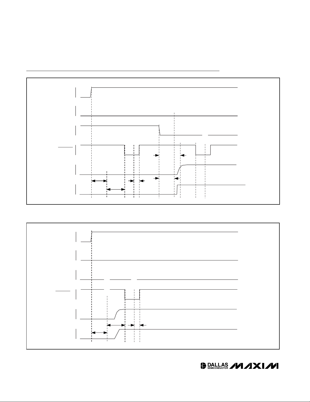
Timing Diagrams
VCC > V
POA
TX-D
I
BIASSET
I
MODSET
t
INIT
P-DOWN/RST
INTERRUPT
RESET-DONE
RESET-DONE
READ-FLAGS
t
INIT ON
t
PDR-OFF
t
INIT OFF
t
INIT
READ-FLAGS
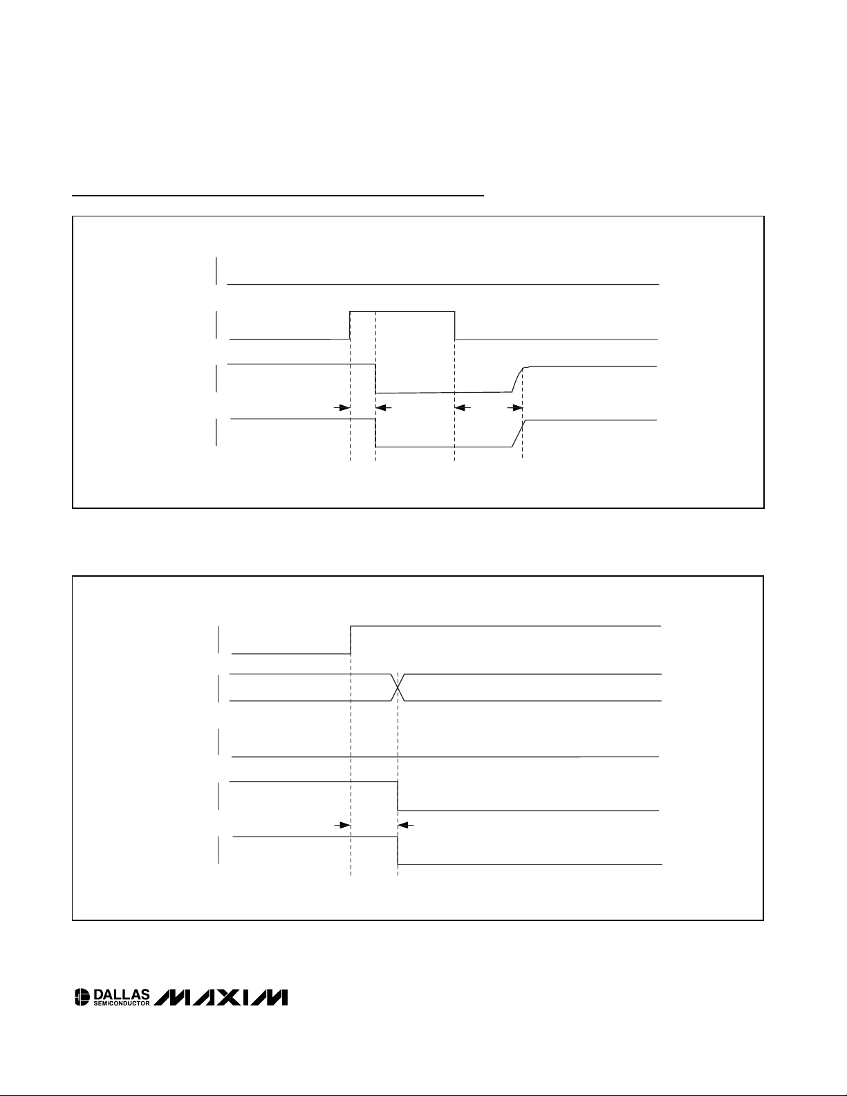
Figure 1. Power-On Initialization with P-DOWN/RST Asserted and TX-D/SOFT-TX-D Not Asserted
Figure 2. Power-On Initialization with P-DOWN/RST Not Asserted and TX-D/SOFT-TX-D Not Asserted (Normal Operation)
VCC > V
POA
TX-D
I
BIASSET
I
MODSET
t
INIT
P-DOWN/RST
INTERRUPT
t
INIT ON
t
INIT OFF
READ-FLAGS
RESET-DONE
Page 9
DS1862
XFP Laser Control and Digital Diagnostic IC
_____________________________________________________________________ 9
Timing Diagrams (continued)
TX-D
TX-F
I
BIASSET
I
MODSET
t
OFF
t
ON
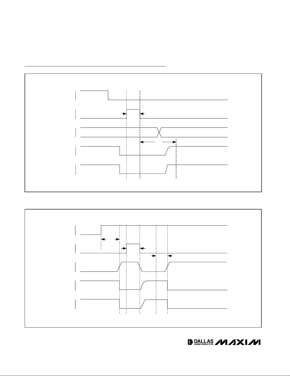
Figure 3. TX-D Timing During Normal Operation
Figure 4. Detection of Safety Fault Condition
TX-D
FETG
OCCURRENCE
OF FAULT
I
BIASSET
I
MODSET
t
FAULT
Page 10
DS1862
XFP Laser Control and Digital Diagnostic IC
10 ____________________________________________________________________
FETG
P-DOWN/RST
OCCURRENCE
OF FAULT
I
BIASSET
I
MODSET
t
RESET
t
INIT
RESET-DONE
Figure 5. Successful Recovery from Transient Safety Fault Condition Using P-DOWN/RST
Figure 6. Unsuccessful Recovery from Transient Safety Fault Condition
FETG
(FETG_POL = 1)
P-DOWN/RST
OCCURRENCE
OF FAULT
I
BIASSET
I
MODSET
t
RESET
t
FAULT
t
FAULT
RESET-DONE
Timing Diagrams (continued)
Page 11
DS1862
XFP Laser Control and Digital Diagnostic IC
____________________________________________________________________ 11
READ FLAGS
OCCURRENCE
OF MONITOR
CHANNEL FAULT
t
INIT_ON
t
INIT_OFF
INTERRUPT
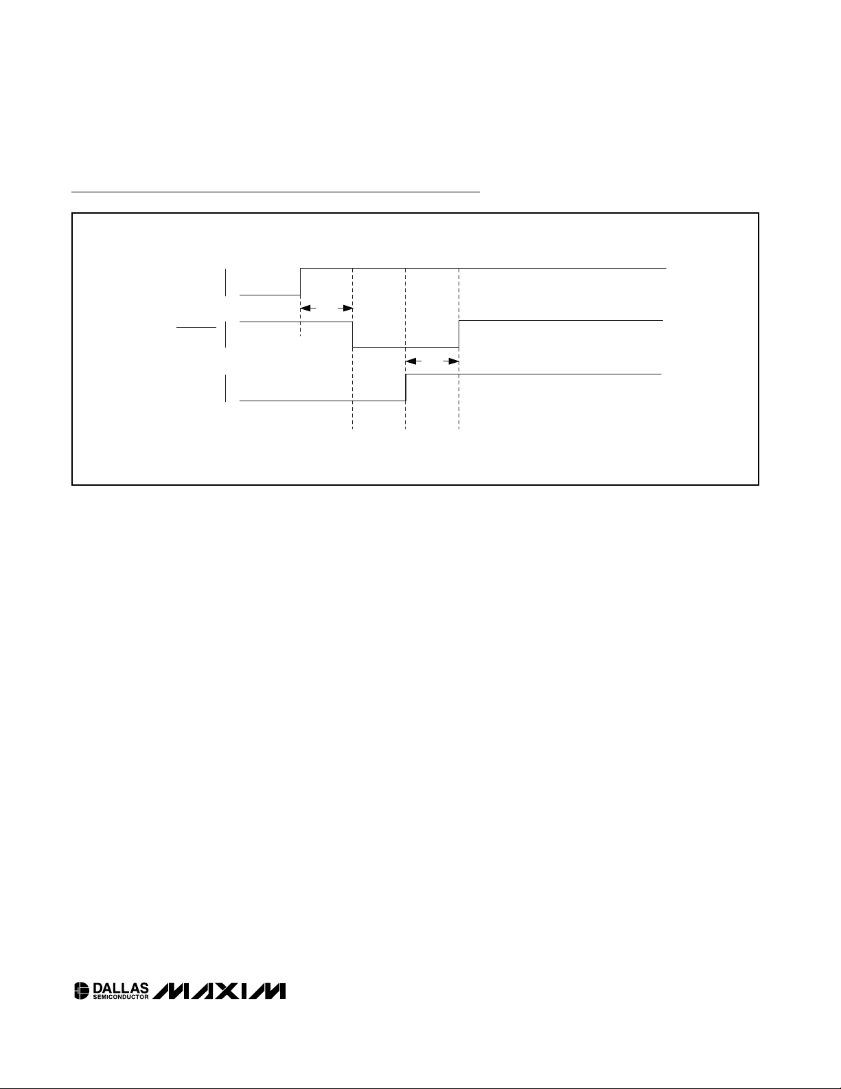
Figure 7. Monitor Channel Fault Timing
Timing Diagrams (continued)
Page 12
DS1862
XFP Laser Control and Digital Diagnostic IC
12 ____________________________________________________________________
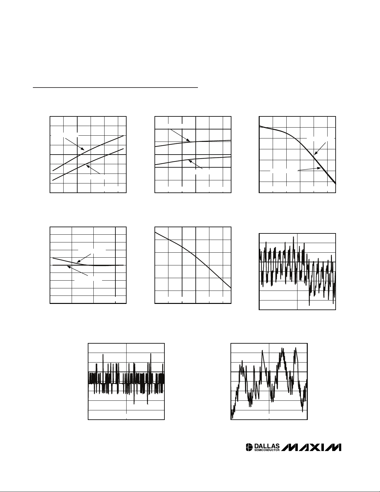
Typical Operating Characteristics
(TA = +25°C, unless otherwise noted.)
SUPPLY CURRENT vs. SUPPLY VOLTAGE
DS1862 toc01
SUPPLY VOLTAGE (V)
SUPPLY CURRENT (mA)
5.34.83.3 3.8 4.3
2.5
3.0
3.5
4.0
4.5
5.0
5.5
6.0
2.0
2.8
SRC_SINK_B = 1
SRC_SINK_B = 0
I
BMD
= 499.479µA
SUPPLY CURRENT vs. TEMPERATURE
DS1862 toc02
TEMPERATURE (°C)
SUPPLY CURRENT (mA)
8560-15 10 35
3.0
3.5
4.0
4.5
5.0
5.5
6.0
-40
SRC_SINK_B = 1
SRC_SINK_B = 0
I
BMD
= 499.479µA
V
CC3
= 5.5V, V
CC2
= 1.6V
I
BMD
DRIFT vs. TEMPERATURE
DS1862 toc03
TEMPERATURE (°C)
I
BMD
DRIFT (%)
8560-15 10 35
-2.5
-1.5
-2.0
-1.0
-0.5
0
0.5
1.0
-40
SRC_SINK_B = 1
SRC_SINK_B = 0
I
BMD
= 499.479µA
V
CC3
= 5.5V, V
CC2
= 1.6V
I
BMD
DRIFT vs. SUPPLY VOLTAGE
DS1862 toc04
SUPPLY VOLTAGE (V)
I
BMD
DRIFT (%)
5.23.6 4.4
-1.0
0
-0.2
0.2
-0.6
-0.8
-0.4
0.4
0.6
0.8
1.0
2.8
SRC_SINK_B = 1
SRC_SINK_B = 0
I
BMD
= 499.479µA
I
MODSET
DRIFT vs. TEMPERATURE
DS1862 toc05
TEMPERATURE (°C)
I
MODSET
DRIFT (%)
85-15 10 35 60
-2.0
-1.5
-1.0
-0.5
0
0.5
1.0
-40
I
BMD
= 499.479µAV
CC3
= 5.5V, V
CC2
= 1.6V
INTEGRAL NONLINEARITY
OF QUICK TRIPS
DS1862 toc06
CODE (0–255)
ERROR (LSB)
256128
-0.8
-0.2
0
-0.6
-0.4
0.2
0.4
0.6
0.8
0
DIFFERENTIAL NONLINEARITY
OF I
MODSET
DS1862 toc07
CODE (0–255)
ERROR (LSB)
256128
-0.20
-0.05
0
-0.15
-0.10
0.05
0.10
0.15
0.20
0
FSR = 75µA
V
CC3
= 4.2V, V
CC2
= 1.6V
INTEGRAL NONLINEARITY
OF I
MODSET
DS1862 toc08
CODE (0–255)
ERROR (LSB)
256128
-0.20
-0.05
0
-0.15
-0.10
0.05
0.10
0.15
0.20
0
FSR = 75µAV
CC3
= 4.2V, V
CC2
= 1.6V
Page 13
DS1862
XFP Laser Control and Digital Diagnostic IC
____________________________________________________________________ 13
Pin Description
NAME
DESCRIPTION
Power-Down/Reset Input. This multifunction pin is pulled high internally. See the Power-Down/Reset Pin
section for additional information.
Signal Conditioner Receiver Loss-of-Signal Input. This pin is an active-high input with LVCMOS/LVTTL
voltage levels.
Signal Conditioner Receiver Loss-of-Lock Input. This pin is an active-high input with LVCMOS/LVTTL
voltage levels.
THRSET
Threshold Set Output. This pin is a programmable voltage source that can be used for Rx signal
conditioner.
V
CC2
1.8V Power-Supply Input
RX-LOS
Receiver Loss-of-Signal. This open-drain output indicates when there is insufficient optical power.
SCL
I2C Serial-Clock Input
FETG
FET Gate Output. This pin can drive an external FET gate associated with safety fault disconnect.
RSSI
Received Power Signal Input
MODSET
Modulation Current Output. This pin is only capable of sinking current.
TX-D
Transmit Disable Input. This pin has an internal pullup resistor.
SDA
I2C Serial-Data Input/Output
EN1
Enable 1 Output. Functional control for signal conditioners.
EN2
Enable 2 Output. Functional control for signal conditioners.
BIASSET
Bias Current Output. This pin is only capable of sinking current.
Interrupt. This open-drain output pin indicates a possible operational fault or critical status condition to the
host.
MOD-NR
Indicating Module Operational Fault. Open-drain output. This pin indicates the status of the MOD-NR flag.
Aux1 Monitor Input. This pin can be used to measure any voltage quantity.
Aux2 Monitor Input. This pin can be used to measure any voltage quantity or external temperature sensor.
BMD
Monitor Diode Current Input. This pin is capable of sourcing or sinking current.
GND
Ground
Module Deselect Input. This pin must be pulled low to enable I2C communication. This pin is pulled high
internally.
IBIASMON
Bias Monitor Input. This pin can be used to monitor the voltage across the laser.
Signal Conditioner Transmitter Loss-of-Signal. This pin is an active-high input with LVCMOS/LVTTL
voltage levels.
V
CC3
3.3V or 5V Power-Supply Input
PIN
P-DOWN/RST A1
SC-RX-LOS A2
SC-RX-LOL A3
A4
A5
B1
B2
B3
B4
B5
C1
C2
C3
C4
C5
INTERRUPT D1
MOD-DESEL E2
SC-TX-LOS E4
D2
AUX1MON D3
AUX2MON D4
D5
E1
E3
E5
Page 14

DS1862
XFP Laser Control and Digital Diagnostic IC
14 ____________________________________________________________________
Block Diagram
MUX
V
CC2
TX-P
LOGIC
SDA
SCL
MOD-DESEL
IBIASMON
RSSI
BMD
AUX1MON
ALARM AND
WARNING
THRESHOLDS
ALARM AND
WARNING
THRESHOLDS
INTERRUPT
WARNING
FLAGS
ALARM
FLAGS
EN1
EN2
RX-LOS
SC-TX-LOS
SC-RX-LOL
SC-RX-LOS
V
CC3
V
CC2
V
CC3
V
CC2
AUX2MON
TX-P
I
BMD
TX-P
HIGH-BIAS ALARM THRESHOLD
HIGH TX_P ALARM THRESHOLD
LOW TX_P ALARM THRESHOLD
I
BIASSET
BIAS AND MOD
ENABLE
TX-F
STARTUP
INITIALIZATION
AND
LASER SAFETY
SHUTDOWN
BLOCK
HIGH-BIAS ALARM
HIGH TX_P ALARM
LOW TX_P ALARM
SOFT TX-D
V
CC2
OR V
CC3
P-DOWN/RST
TX-D
FETG
INT
GAIN
ALARM FLAGS
WARNING FLAGS
MASKING BITS
ADC 13 BIT
OFFSET
RIGHT
SHIFTING
I2C
INTERFACE
MEASURED DATA
COMPARATORS
V
CC3
V
CC3
INTERRUPT
MOD-NR
GND
LOWER MEMORY
ADDRESS
R/W
DATA BUS
ADDRESS
R/W
DATA BUS
INT
TABLE-SELECT BYTE
TABLE
01h
SERIAL ID
DATA
TABLE
02h
EEPROM
TABLE
03h
LUT
TABLE
05h
THRSET
TABLE
04h
MODULE
CONFIG
THRSET
MODSET
BIASSET
HIGH-BIAS QT
I
BMD
A
EXT(IBMD
)
BIAS AND
MODULATION
ENABLE
MASKING BITS
R
PU
R
PU
R
PU
MISC
CONTROL
SIGNALS
TEMPERATURE
CONTROLED
WITH
LUT
TEMPERATURE
SENSOR
V
CC3
I TO V
A
DS1862
Page 15

DS1862
XFP Laser Control and Digital Diagnostic IC
____________________________________________________________________ 15
Detailed Description
The DS1862’s block diagram is described in detail
within the following sections and memory map/memory
description.
Automatic Power Control (APC)
The DS1862’s APC is accomplished by closed-loop
adjustment of the bias current (BIASSET) until the feedback current (BMD) from a photodiode matches the
value determined by the APC registers. The relationship between the APC register and I
BMD
is given by:
I
BMD
= 5.859µA x APCC<7:0> +
(1.464µA x APCF<1:0>)
where APCC<7:0> is the 8-bit value in Table 04h, byte
84h that controls the coarse BMD current and
APCF<1:0> is the 2-bit value that controls the fine BMD
current.
The BMD pin appears as a voltage source in series with
two resistors. The overall equivalent resistance of the
BMD input pin can be closely approximated by the plot
in Figure 8. The voltage that appears on the BMD pin,
assuming no external current load, is 1.2V if BMD is in
sink-current mode (SRC_SINK_B = 0) or 2.0V if BMD is
set to source current (SRC_SINK_B = 1). This allows the
photodiode to be referenced to either V
CC3
or GND.
When the control loop is at steady state, the BMD current
setting matches the current that is measured by the I
BMD
voltage across the internal resistance. During a transient
period, the DS1862 adjusts the current drive on the
BIASSET pin to bring the loop into steady state. The
DS1862 is designed to support loop gains of 1/20 to 10.
On power-up, the BMD current ramps up to the previously saved current setting in EEPROM APC registers.
While operating, the DS1862 monitors the BMD current.
If it begins to deviate from the desired (set) I
BMD
value,
then, again, the current on the BIASSET pin is adjusted
to compensate.
Extinction Ratio Control
Look-Up Table (LUT)
The DS1862 uses a temperature indexed look-up table
(LUT) to control the extinction ratio. The MODSET pin is
capable of sinking current based on the 8-bit binary
value that is controlling it. The DS1862 also features a
user-configurable current range to increase extinction
ratio resolution. Five current ranges, as described in
Table 1, are available to control the current entering
MODSET.
I
BMD
VOLTAGE
BMD
NOTE: V
BMD
IS
CONTROLLED BY THE
SRC_SINK BIT IN
TABLE 04h
I
BMD
(mA)
R
BMD
(Ω)
1.501.250.25 0.50 0.75 1.00
BMD RESISTANCE vs. BMD SUPPLY CURRENT
470
489
508
527
546
565
584
600
0
0
V
BMD
R
BMD
Figure 8. Approximate Model of the BMD Input
Table 1. Selectable Current Ranges for
MODSET
LUT CURRENT RANGE
TABLE 04h, BYTE 86h<2:0>
CURRENT RANGE
(µA)
000 0 to 75
001 0 to 150
010 0 to 300
011 0 to 600
100 0 to 1200
Page 16

DS1862
XFP Laser Control and Digital Diagnostic IC
16 ____________________________________________________________________
If the largest current range is selected, the maximum
value of FFh (from LUT) corresponds to a 1200µA sink
current. Regardless of current range, the MODSET
value always consists of 256 steps, including zero.
I
MODSET
can be controlled automatically with the temperature-based look-up table, or by three other manual
methods.
Automatic temperature addressed look-up is accomplished by an internal or external temperature sensor
controlling an address pointer. This pointer indexes
through 127 previously loaded 8-bit current values
stored in the LUT. Each one of the 127 temperature
slot locations corresponds to a 2°C increment over
the -40°C to +102°C temperature range. Any temperature above or below these points causes the code in
the first or last temperature slot to be indexed. Both the
internal temperature sensor and an external sensor
connected to AUX2MON are capable of providing a
signal to control the extinction ratio automatically with
an indexed LUT. Table 2 illustrates the relationship
between the temperature and the memory locations in
the LUT.
Automatic and manual control of MODSET is controlled
by two bits: TEN and AEN that reside in Table 04h, Byte
B2h. By default (from factory) TEN and AEN are both
set, causing complete automatic temperature-based
look-up. If TEN and/or AEN are altered, then the
DS1862 is set to one of the manual modes. Table 3
describes manual mode functionality.
Table 2. Temperature Look-Up Table
TEMPERATURE (°C)
CORRESPONDING LOOK-UP
TABLE ADDRESS
< -40 80h
-40 80h
-38 81h
-36 82h
——
+96 C4h
+98 C5h
+100 C6h
+102 C7h
> +102 C7h
Table 3. Truth Table for TEN and AEN Bits
TEN
DS1862 LUT FUNCTIONALITY
0
Manual mode that allows users to write a value
directly to the LUT Value register (Table 04h,
Byte B1h) to drive MODSET. While in this mode,
the LUT index pointer register is not being
updated, and no longer drives the LUT Value
register.
0
Manual mode that allows users to write a value
directly to the LUT Value register (Table 04h,
Byte B1h) to drive MODSET. While in this mode,
the LUT index pointer register is still being
updated, however it no longer drives the LUT
Value register.
1
Manual mode that allows users to write a value to
the LUT index pointer (Table 04h, Byte B0), then
the DS1862 updates the LUT Value register
(Table 04h, Byte B1h) based on the user’s index
pointer.
1
Automatic mode (factory default). This mode
automatically indexes the LUT based on
temperature, placing the resulting LUT address
in the LUT index pointer register (Table 04h, Byte
B0h). Then the MODSET setting is transferred
from that LUT address to the LUT Value register
(Table 04h, Byte B1h). Lastly the I
MODSET
is set
to the new MODSET code.
AEN
0
1
0
1
Page 17

DS1862
XFP Laser Control and Digital Diagnostic IC
____________________________________________________________________ 17
Monitor Channels
The DS1862 has seven monitored voltage signals that
are polled in a round-robin multiplexed sequence and
are updated with the frame rate, t
FRAME
. All channels
are read as 16-bit values, but have 13-bit resolution,
and with the exception of temperature measurements,
all channels are stored as unsigned values. The resulting
16-bit value for all monitored channels, except internal
temperature, is calculated by internally averaging the
analog-to-digital result 8 times. The resulting internal
temperature monitor channel is averaged 16 times. See
the Internal Calibration section for a complete descrip-
tion of each channel’s method(s) of internal calibration.
The AUX1MON, AUX2MON, and V
CC2/3
monitor channels are optional and can be disabled. This feature
allows for shorter frame rate for the essential monitor
channels. Channels that can not be disabled are: internal temperature, BMD, RSSI, and IBIASMON. A table of
full-scale (FS) signal values (using factory internal calibration without right shifting) and the resulting FS code
values for all seven channels is provided below.
Measuring Temperature—Internal or External
The DS1862 is capable of measuring temperature on
three different monitor channels: internal temperature
sensor, AUX1MON, and AUX2MON. Only the internal
temperature and AUX2MON channels are capable of
indexing the LUT to control the extinction ratio. To use
an external temperature sensor on AUX2MON, the
TEMP_INT/EXT bit in Table 04h, Byte 8Bh, must be set.
While AUX2MON controls the extinction ratio, the internal temperature sensor does not stop running; despite
extinction ratio control by AUX2MON, it is this internal
temperature signal that continues to control the status
of temperature flags. Also when TEMP_INT/EXT = 1, the
internal temperature clamps at -40°C and +103.9375°C,
and when TEMP_INT/EXT = 0 it clamps at -120°C and
+127.984°C. AUX2MON, however, does have its own flag
to indicate an out-of-tolerance condition and assert the
INTERRUPT pin.
Both AUX1MON and AUX2MON can be used to measure temperature as a function of voltage on their
respective pins. They can be enabled by selecting
either 0h or 4h from Table 5. Internal (or external) calibration may be required to transmute the input voltage
to the desired two’s-complement digital code, readable
from the result registers in lower memory, Bytes 6Ah,
6Bh and 6Ch, 6Dh.
Measuring V
CC2/3
The DS1862 has the flexibility to internally measure
either V
CC2
or V
CC3
to monitor supply voltage. V
CC2
or
V
CC3
is user selectable by the V
CC2/3
_Sel bit in Table
01h, Byte DCh. To remove V
CC2/3
from the round-robin
monitor update scheme, despite having V
CC2
or V
CC3
selected to be monitored, the Reserve_EN bit in Table
04h, Byte 8Bh can be programmed to a 0. The analog
power-on-reset flag, POA, indicates the status of V
CC3
power supply. Even though POA seems to behave similarly to V
CC2/3
monitor channel, it is completely sepa-
rate and has no connection.
Measuring APC and Laser Parameters—BMD,
IBIASMON, RSSI
BMD and BIASSET are used to control and monitor the
laser functionality. Regardless of the set BMD current in
the APC register, the DS1862 measures BMD pin current and uses this value not only to adjust the current
on the BIASSET pin, but also to monitor TX-P as well.
The IBIASMON pin is used to input a voltage signal to
the DS1862 that can be used to monitor the bias current through the laser. This monitor channel does not
drive the HIGHBIAS quick-trip (QT) alarms for safety
Table 4. Monitor Channel FS and LSB Detail
SIGNAL +FS SIGNAL +FS (hex) -FS SIGNAL -FS (hex) LSB
Temperature 127.984°C 7FF8 -120°C 8800 0.0625°C
V
CC2/3
6.5528V FFF8 0V 0000 100µV
IBIASMON 2.4997V FFF8 0V 0000 38.147µV
RSSI 2.4997V FFF8 0V 0000 38.147µV
AUX1MON 6.5528V FFF8 0V 0000 38.147µV
AUX2MON 6.5528V FFF8 0V 0000 38.147µV
BMD (TX-P) 1.5mA FFF8 0mA 0000 22.888nA
RESERVE_EN V
00V
01V
10V
11V
CC2/3_Sel
RESULT
result not enabled.
CC2/3
result not enabled.
CC2/3
is being measured.
CC3
is being measured.
CC2
Page 18

DS1862
XFP Laser Control and Digital Diagnostic IC
18 ____________________________________________________________________
fault functionality, current on the BIASSET pin is monitored by the DS1862 to control the HIGHBIAS quick
trip. Similar to TX-P, the RSSI pin is used to measure
the received power, RX-P.
Measuring Voltage Quantities
using AUX1MON and AUX2MON
AUX1MON and AUX2MON are auxiliary monitor inputs
that may be used to measure additional parameters.
AUX1/2MON feature a user-selectable register that
determines the measured value’s units (i.e., voltage,
current, or temperature). In addition to indicating units,
some of the 4-bit op-codes, in Table 5, also place the
part in special modes used for alarms and faults internally. Whichever units’ scale is selected, the DS1862 is
only capable of measuring a positive voltage quantity,
therefore internal or external calibration may be
required to get the binary value to match the measured
quantity. A table of acceptable units and/or their corresponding user-programmable 4-bit op-code is provided below.
Alarms and Warning Flags
Based on Monitor Channels
All of the monitor channels feature alarm and warning
flags that are asserted automatically as user-programmed thresholds are internally compared with monitor channel results. Flags may be set, which, if not
masked, will generate an interrupt on the INTERRUPT
pin or generate a safety fault. Whenever V
CC2/3
,
AUX2MON, AUX1MON, RSSI, and internal temperature
go beyond their threshold trip points and the corresponding mask bit is 0, an interrupt is generated on the
INTERRUPT pin and a corresponding warning or alarm
flag is set. Similarly, a safety fault occurs whenever
BMD or BIASSET go beyond threshold trip points.
When this happens, the FETG pin immediately asserts
and BIASSET and MODSET currents are shut down.
Monitor Channel Conversion Example
Table 6 provides an example of how a 16-bit ADC code
corresponds to a real life measured voltage using the
factory-set calibration on either RSSI or IBIASMON. By
factory default, the LSB is set to 38.147µV.
To calculate V
CC2
, V
CC3
, AUX1MON, or AUX2MON,
convert the unsigned 16-bit value to decimal and multiply by 100µV.
To calculate the temperature (internal), treat the two’scomplement value binary number as an unsigned binary number, then convert it to decimal and divide by
256. If the result is grater than or equal to 128, subtract
256 from the result.
Temperature: high byte = -128°C to +127°C signed;
low byte = 1/256°C.
Table 5. AUX1/2MON Functionality
Selection (Unit Selection)
VALUE
DESCRIPTION OF AUX1/2MON INTENDED USE
(UNITS OF MEASURE)
Auxiliary monitoring not implemented
APD bias voltage (16-bit value is voltage in units of
10mV)
Reserved
TEC current (mA), (16-bit value is current in units of
0.1mA)
Laser temperature (same encoding as module
temperature)
Laser wavelength
+5V supply voltage (encoded as primary voltage
monitor)
+3.3V supply voltage (encoded as primary voltage
monitor)
+1.8V supply voltage (encoded as primary voltage
monitor) (V
CC2
)
-5.2V supply voltage (encoded as primary voltage
monitor)
+ 5V sup p l y cur r ent ( 16- b i t val ue i s cur r ent i n 0.1m A)
+3.3V supply current (16-bit value is current in
0.1mA)
+1.8V supply current (16-bit value is current in
0.1mA)
-5.2V supply current (16-bit value is current in
0.1mA)
Table 6. A/D Conversion Example
MSB (BIN) LSB (BIN) VOLTAGE (V)
11000000 00000000 1.875
10000000 10000000 1.255
Table 7. Temperature Bit Weights
S262
5
2
4
2
3
2
2
2
1
2
0
2
-1
2
-2
2
-3
2
-4
2
-5
———
0000b
0001b
0010b
0011b
0100b
0101b
0110b
0111b
1000b
1001b
1010b
1101b
1110b
1111b
Page 19

DS1862
XFP Laser Control and Digital Diagnostic IC
____________________________________________________________________ 19
Internal Calibration
The DS1862 has two means for scaling an analog input
to a digital result. The two devices alter the gain and
offset of the signal to be calibrated. All of the inputs
except internal temperature have unique registers for
both the gain and the offset that can be found in Table
04h. See the table below for a complete description of
internal calibration capabilities including right-shifting
for all monitor channels.
To scale a specific input’s gain and offset, the relationship between the analog input and the expected digital
result must be known. The input that would produce a
corresponding digital result of all zeroes is the null
value (normally this input is GND). The input that would
produce a corresponding digital result of all ones is the
full-scale (FS) value minus one LSB. The FS value is
also found by multiplying an all ones digital value by
the weighted LSB. For example, a digital reading is 16
bits long, assume that the LSB is known to be 50µV,
then the FS value would be 2
16
x 50µV = 3.2768V.
A binary search can be used to find the appropriate
gain value to achieve the desired FS of the converter.
Once the gain value is determined, then it can be
loaded into the appropriate channels’ Gain register.
This requires forcing two known voltages on to the
monitor input pin. For best results, one of the forced
voltages should be the NULL input and the other
should be 90% of FS. Since the LSB of the least significant bit in the digital reading register is known, the
expected digital results are also known for both the null
and FS value inputs. Figure 9 describes the hysteresis
built into the DS1862’s LUT functionality.
With the exception of BMD, which can source or sink
current, all monitored channels are high impedance
and are only capable of directly measuring a voltage. If
other measured quantities are desired, such as: light,
frequency, power, current etc., they must be converted
to a voltage. In this situation the user is not interested in
voltage measurement on the monitored channel, but
the measurement of the desired parameter. Only the
relationship between the indirect measured quantity
(light, frequency, power, current, etc.) to the expected
digital result must be known.
An example of gain scaling using the recommended
binary search procedure is provided with the following
pseudo-code.
To help will the computation, two integers need to be
defined: count 1 and count 2. CNT1 = NULL / LSB and
CNT2 = 90%FS / LSB. CLAMP is the largest result that
can be accommodated.
Table 8. Temperature Conversion
Examples
MSB (BIN) LSB (BIN) TEMPERATURE (°C)
01000000 00000000 +64
01000000 00001000 +64.03215
01011111 00000000 +95
11110110 00000000 -10
11011000 00000000 -40
Table 9. Internal Calibration Capabilities
SIGNAL
INTERNAL
SCALING
INTERNAL
OFFSET
RIGHT-
SHIFTING
Temperature
—x—
V
CC2/3
xx—
IBIASMON x x x
RSSI (RX-P) x x x
AUX1MON x x x
AUX2MON x x x
BMD (TX-P) x x x
Figure 9. Look-Up Table Hysteresis
M6
M5
M4
M3
MEMORY LOCATION
M2
M1
DECREASING
TEMPERATURE
INCREASING
TEMPERATURE
2 4 6 8 10 12
TEMPERATURE (°C)
Page 20

DS1862
XFP Laser Control and Digital Diagnostic IC
20 ____________________________________________________________________
/* Assume that the Null input is 0.5V. */
/* In addition, the requirement for LSB is 50µV. */
FS = 65536 * 50e-6; /* 3.2768 */
CNT1 = 0.5 / 50e-6; /* 10000 */
CNT2 = 0.90*FS / 50e-6; /* 58982 */
/* Thus the NULL input of 0.5V and the 90% of FS input
is 2.94912V. */
set the trim-offset-register to zero;
set Right-Shift register to zero (Typically zero.
See the Right-Shifting section);
gain_result = 0h;
CLAMP = FFF8h/2^(Right_Shift_Register);
For n = 15 down to 0
begin
gain_result = gain_result + 2^n;
Force the 90% FS input (2.94912V);
Meas2 = read the digital result from the part;
If Meas2 >= CLAMP then
gain_result = gain_result - 2^n;
Else
Force the NULL input (0.5V);
Meas1 = read the digital result from the part;
if (Meas2 - Meas1) > (CNT2 - CNT1) then
gain_result = gain_result - 2^n;
end;
Set the gain register to gain_result;
The gain register is now set and the resolution of the
conversion will best match the expected LSB. The next
step is to calibrate the offset of the DS1862. With the
correct gain value written to the gain register, again
force the NULL input to the monitor pin. Read the digital result from the part (Meas1). The offset value is
equal to negative value of Meas1.
The calculated offset is now written to the DS1862 and
the gain-and offset-scaling procedure is complete.
Right-Shifting A/D Conversion Result
(Scalable Dynamic Ranging)
Right-shifting is a digital method used to regain some
of the lost ADC range of a calibrated system. If rightshifting is enabled, by simply loading a non-zero value
into the appropriate Right-Shifting Register, then the
DS1862 shifts the calibrated result just before it is
stored into the monitor channels’ register. If a system is
calibrated so the maximum expected input results in a
digital output value of less than 7FFFh (50% of FS),
then it is a candidate for using the right-shifting
method.
If the maximum desired digital output is less than
7FFFh, then the calibrated system is using less than 1/2
the ADC’s range. Similarly, if the maximum desired digital output is less than 1FFFh, then the calibrated system is only using 1/8th the ADC’s range. For example, if
an applied maximum analog signal yields a maximum
digital output less than 1FFCh, then only 1/8th of the
ADC’s range is used. Right-shifting improves the resolution of the measured signal as part of internal calibration. Without right-shifting, the 3 MS bits of the ADC will
never be used. In this example, a value of 3 for the
right-shifting maximizes the ADC range and a larger
gain setting must be loaded to achieve optimal conversion. No resolution is lost since this is a 13-bit converter
that is left justified. The value can be right-shifted 3
times without losing any resolution. The following table
describes when the right-shifting method can be effectively used.
OFFSET REGISTER
MEAS
_
()
=
−
⎡
⎣
⎢
⎤
⎦
⎥
11
4
Table 10. Right-Shifting Selection
OUTPUT RANGE USED WITH
ZERO RIGHT-SHIFTS
NUMBER OF RIGHT-
SHIFTS NEEDED
0h .. FFFFh 0
0h .. 7FFFh 1
0h .. 3FFFh 2
0h .. 1FFFh 3
0h .. 0FFFh 4
Page 21

DS1862
XFP Laser Control and Digital Diagnostic IC
____________________________________________________________________ 21
Warning and Alarm Logic Based on
AUX1/2MON, V
CC2/3
, Temp, RX-P,
and IBIASMON
The DS1862 is capable of generating an alarm and/or
warning whenever an analog monitored channel goes
out of a user-defined tolerance. Temperature, bias current (based on IBIASMON), receive power (based on
RSSI), AUX1MON, AUX2MON, and V
CC2/3
, are moni-
tored channels that generate latched flags. See the figure below for more detail pertaining to AUX1MON and
AUX2MON. Flags are latched into a high state the first
time a monitored channel goes out of the defined operating window and for each monitored signal there is a
Mask bit that can be set to prevent the corresponding
alarm or warning flag from being set. Once a flag is set,
it is cleared by simply reading its memory location.
AUX1/2MON LOGIC
AUX1MON (PIN)
AUX2MON (PIN)
MASK BIT
AUX1MON
AUX2MON
ADC
THRESHOLD
AUX1MON
(APD MODE)
LATCHED-APDSUPPLY-FAULT
AUX2MON
(APD MODE)
INTERRUPT (PIN)
*COMPARATOR LOGIC IS
DUPLICATED FOR HIGH
AND LOW ALARMS AND
WARNINGS.
C
ADC
THRESHOLD
C
4-BIT UNIT SELECT
LATCH
AUX1MON
(LASER WL MODE)
LATCHEDWAVELENGH-UL
AUX2MON
(LASER WL MODE)
LATCH
AUX1MON
(V
EE5
MODE)
LATCHED-V
EE5
AUX2MON
(V
EE5
MODE)
LATCH
AUX1MON
(V
CC2
MODE)
LATCHED-V
CC2
AUX2MON
(V
CC2
MODE)
LATCH
AUX1MON
(TEC MODE)
LATCHED-TECFAULT
AUX2MON
(TEC MODE)
LATCH
AUX1MON
(V
CC5
MODE)
LATCHED-V
CC5
AUX2MON
(V
CC5
MODE)
LATCH
AUX1MON
(V
CC3
MODE)
LATCHED-V
CC3
AUX2MON
(V
CC3
MODE)
LATCH
ANY FLAG
CORRESPONDING MASK
BIT
Figure 10. AUX1/2 Monitor Logic
Page 22

DS1862
XFP Laser Control and Digital Diagnostic IC
22 ____________________________________________________________________
Warning and Alarm Logic Based on
Signal Conditioners
The DS1862 also has flags that are set by certain logical
conditions on signal conditioner (SC) pins: SC-RX-LOL,
SC-RX-LOS, SC-TX-LOS. Similarly, for each latched
signal conditioner flag there are also mask bits that are
capable of preventing the alarm or warning flag from
causing an INTERRUPT pin to assert. Again, flags are
cleared automatically whenever their memory address
is read. See Figure 11 for more detail.
Quick-Trip Logic and FTEG
Shutdown Functionality
In addition to alarms and warnings, the DS1862 also
has quick-trip (QT) functionality (sometimes referred to
as fast alarms) that is capable of shutting down the
LASER with the FETG pin in conjunction with shutting
down I
MODSET
and I
BIASSET
. I
BMD
and I
BIASSET
currents are measured and are compared with userdefined trip points to set the quick-trip flags: QT LOW
TX-P, QT HIGH TX-P, and QT HIGH BIAS. These flags
are also capable of being masked to prevent FETG
from being asserted when an out-of-tolerance condition
is detected. FETG is not asserted by setting the TX-D
pin, SOFT TX-D, or P-DOWN/RST pin to a high state,
however, I
MODSET
, and I
BIASSET
will shut down. See
Figure 12 for more detail.
SIGNAL CONDITIONER AND MISCELLANEOUS LOGIC
ANY FLAG
ANY MASK BIT
HIGH TX-P
LOW TX-P
LATCHED-TX-FAULT
HIGH BIAS
INTERRUPT (PIN)
TIMER
LATCH
SC-RX-LOS
(PIN)
LATCHED-RX-NR
SC-RX-LOL
(PIN)
LATCH
SC-TX-LOS
(PIN)
LATCHED-TX-NR
LATCHED-TX-FAULT
LATCH
P-DOWN/RST
(PIN)
LATCHED-RESET-DONE
LATCHED
RX-CDR-NL
LATCHLATCH
SC-RX-LOL
(PIN)
LATCHEDRX-LOS
RX-LOS (PIN)
*OPEN DRAIN
LATCH
SC-RX-LOS
(PIN)
SC-RX-LOL (PIN)
TX-FAULT
LATCHEDMOD-NR
VCC2-FAULT
*OPEN DRAIN
MOD-NR (PIN)
LATCH
Figure 11. Signal Conditioner and Other Logic
Page 23

DS1862
XFP Laser Control and Digital Diagnostic IC
____________________________________________________________________ 23
The polarity of the FETG pin can also be reversed by
setting the FETG_POL bit. Once a safety fault has
occurred, the FETG pin and all of the attendant flags can
only be reset by pulsing the P-DOWN/RST pin high for the
reset time, t
RESET
, or by toggling the P-DOWN/RST bit in
Byte 6Eh, bit 4. See the Power-Down/Reset Pin section for
more details.
Power-Down/Reset Pin
The P-DOWN/RST pin is a multifunction input pin that
resets and/or powers down the DS1862. Since the pin is
internally pulled up, its normal state is released, which
corresponds to power-down mode. If the P-DOWN/RST
pin is released, or driven high, the DS1862 responds by
shutting down the MODSET and BIASSET currents.
Once the pin is pulled low, operation continues (if not
inhibited by a safety fault). Besides powering down the
DS1862, a high-going pulse with minimum reset time,
t
RESET
, can be applied to the P-DOWN/RST pin. This is
necessary to restart the DS1862, especially if it is in a
safety shutdown condition and needs to be restarted
after the safety condition has been rectified. See the
timing diagrams for proper pin timing.
Power-Down Functionality
During power-down mode I
BIASSET
and I
MODSET
drop
below 10µA, effectively shutting down the laser. FETG
is not asserted and safety faults do not occur during
this period. During power-down, I2C communication is
still active, but the signal conditioner pins EN1 and EN2
are noncontrollable and automatically change to the
states: EN1 = 1 and EN2 = 0. Other internal flags/signals that are based on the signal conditioner inputs still
reflect the status on the signal conditioner pins during
power-down. For example, RX-LOS still reflects the status of SC-RX-LOS, and MOD-NR still reflects the logical
states for the signal conditioner pins. Similarly, it is possible for FETG to be asserted, even though the BIASSET
and MODSET currents are shut down. However, during
power-down and a short period, t
PDR-OFF
, during powerup, TX-P Low flag is ignored (internally automatically
masked out) and does not contribute to FETG’s logic.
SHUTDOWN LOGIC
BMD (PIN)
(TX-P CURRENT)
BMD (PIN)
(TX-P CURRENT)
LOW TX-P MASK
HIGH TX-P MASK
QT LOW
TX-P FLAG
QT HIGH
TX-P FLAG
ADC
THRESHOLD
ADC
THRESHOLD
BIAS HIGH MASK
QT BIAS
HIGH FLAG
BIASSET (PIN)
(BIASSET CURRENT)
ADC
THRESHOLD
SOFT TX-D
P-DOWN/RST (PIN)
TX-D (PIN)
SHUTDOWN
FLAG
SAFETY FLAG
SOFT P-DOWN/RST
QT LOW TX-P FLAG
QT HIGH TX-P FLAG
SAFETY FLAG
FETG_POL
DRIVE A P-CHANNEL SWITCH
DRIVE A N-CHANNEL SWITCH
0
1
QT BIAS HIGH FLAG
LATCH
LATCHED-TX-FAULT
LATCH
FETG (PIN)
FETG_POL
Figure 12. Safety Fault and Shutdown Logic
Page 24

DS1862
XFP Laser Control and Digital Diagnostic IC
24 ____________________________________________________________________
During an asserted period of P-DOWN/RST (DS1862 in
power-down), and V
CC3
is cycled, the DS1862 remains
in power-down mode upon power-up. While in powerdown mode the INTERRUPT pin does not assert. Once
V
CC3
has returned, the reset done flag asserts after the
interrupt assert delay, t
INIT ON
.
Reset Functionality
Besides powering down the DS1862, the P-DOWN/RST
pin also functions to reset the DS1862. After a highgoing pulse of time t
RESET
, several events occur within
the DS1862. First, MODSET and BIASSET currents shut
down and are then reinstated. Second, between the rising edge of the reset pulse and the assertion of the
reset-done flag (t
INIT
), the low TX-P flag is ignored and
does not cause FETG to trip. After time t
INIT,
the low
TX-P flag becomes functional. Also, at this time, the
reset-done flag is asserted, causing an interrupt to be
generated. If there are no faults before t
INIT
, then no
interrupts are asserted on the INTERRUPT pin.
If V
CC3
is powered up while P-DOWN/RST is high, then
the reset-done flag must be cleared twice. The first time
the reset-done flag is generated by V
CC3
powering up,
the second time reset-done is generated by a falling
edge on P-DOWN/RST. If V
CC3
is continuously powered while P-DOWN/RST is low then only one resetdone flag needs to be cleared. See the timing
diagrams for graphical detail.
DS1862 Memory Map
Memory Organization
The DS1862 features six separate memory tables that
are internally organized into four byte rows. The Lower
Memory is addressed from 00h to 7Fh and contains
alarm and warning thresholds, flags, masks, several
control registers, password entry area (PE), and the
Table Select byte. Table 01h primarily contains user
EEPROM as well as several control bytes for various
functions. Table 02h is strictly user EEPROM that is protected by a host password. Table 03h is strictly used
for controlling the extinction ratio with an LUT. Table
04h is a multifunction space that contains internal calibration values for monitored channels, LUT index pointers, and miscellaneous control bytes. Table 05h is
factory programmed and stores SCALE values for use
with suggested external temperature sensors. Also, one
byte in Table 05h controls the THRSET voltage source
and is completely accessible without any password
protection. See the Memory section for a more complete detail of each byte’s function, as well as Table 11
for read/write permissions for each Byte. Many nonvolatile memory locations (listed within the Detailed
Register Description section) are actually SRAMShadowed EEPROM, which are controlled by the SEEB
bit in Table 4, Byte B2h.
The DS1862 incorporates SRAM-shadowed EEPROM
memory locations for key memory addresses that may
be rewritten many times. By default the Shadowed
EEPROM Bit, SEEB, is not set and these locations act
as ordinary EEPROM. By setting SEEB, these locations begin to function like SRAM cells, which allow an
infinite number of write cycles without concern of wearing out the EEPROM. This also eliminates the requirement for the EEPROM write time, tWR. Because
changes made with SEEB enabled do not affect the
EEPROM, these changes are not retained through
power cycles. The power-up value is the last value written with SEEB disabled. This function can be used to
limit the number of EEPROM writes during calibration or
to change the monitor thresholds periodically during
normal operation helping to reduce the number of times
EEPROM is written. The Memory Map description indicates which locations are shadowed-EEPROM.
Page 25

DS1862
XFP Laser Control and Digital Diagnostic IC
____________________________________________________________________ 25
DEC hex
00
I
2
C SLAVE ADDRESS A0h
127 7F
128 80
TABLE SELECT BYTE
255 FF
TABLE 01h
TABLE 00h
TABLE 02h
TABLE 04hTABLE 03h
80h
C7h
CONTROL AND
CONFIGURATION
TABLE
(72 BYTES)
MODULATION DAC
LUT
USER EEPROM DATA
80h 80h80h
BBh
FFh
XFP MSA
SERIAL ID DATA
PASSWORD ENTRY (PWE)
(4 BYTES)
00h
7Fh
LOWER MEMORY
DIGITAL DIAGNOSTIC
FUNCTIONS
TABLE 05h
OPTIONAL SCALE VALUES
AND THRSET CONTROL
80h
87h
FFh
DC220 MISC CONTROL BITS
Figure 13. General View of DS1862 Memory Organization
Register Map
Table 11. Permission Table
PERMISSION
READ WRITE
<0>
At least one byte in this row is different than
the rest of the bytes, so look at each byte
separately for permissions.
<1> ALL ALL
<2> ALL MODULE
<3> ALL HOST
<4> MODULE MODULE
<5> ALL FACTORY
<6> NEVER HOST
<7> NEVER MODULE
Page 26

DS1862
XFP Laser Control and Digital Diagnostic IC
26 ____________________________________________________________________
LOWER MEMORY (00H–7FH)
WORD 0 WORD 1 WORD 2 WORD 3
A D DR ESS
( h ex )
BYTE 0/8 BYTE 1/9 BYTE 2/A BYTE 3/B
BYTE 5/D BYTE 6/E
BYTE 7/F
00
<0,2>
EE Signal Cond Temp Alarm Hi Temp Alarm Lo Temp Warn Hi
08
<2>
Temp Warn Lo V
CC3
Alarm Hi* V
CC3
Alarm Lo* V
CC3
Warn Hi*
10
<2>
V
CC3
Warn Lo* Bias Alarm Hi Bias Alarm Lo Bias Warn Hi
18
<2>
Bias Warn Lo TX-P Alarm Hi TX-P Alarm Lo TX-P Warn Hi
20
<2>
TX-P Warn Lo RX-P Alarm Hi RX-P Alarm Lo RX-P Warn Hi
28
<2>
RX-P Warn Lo Aux1 Alarm Hi Aux1 Alarm Lo Aux1 Warn Hi
30
<2>
Aux1 Warn Lo Aux2 Alarm Hi Aux2 Alarm Lo Aux2 Warn Hi
38
<0,2>
Aux2 Warn Lo EE EE
Reserved Reserved Reserved
40
<1>
Reserved Reserved Reserved Reserved
Reserved SRAM SRAM
48
<1>
SRAM SRAM SRAM SRAM SRAM SRAM SRAM SRAM
50
<1>
TxP Alarm
Res Alarm
TxP Warn
RxP/Aux1/Aux2/
Res Warn
Tx/Rx Misc
Flags
Apd/Tec/
V
CC5/3/2
Vee
V
CC5/3/2
Vee
Warn Flags
58
<1>
TxP Mask
Res Mask
TxP Mask
Res Mask
Rx/Rx Misc
Mask
Res Mask
V
CC5/3/2/
Vee
V
CC5/3/2
/Vee
Warn Mask
60
<1>
Temp Value V
CC2/3
Value* Bias Value TX-P Value
68
<1>
RX-P Value Aux1 Value Aux2 Value GCS1 GCS0
70
<0,1>
Reserved Reserved Reserved Reserved POA Reserved PEC_EN Host PW
78
<0,1>
Host PW Host PW Host PW PWE (MSB) PWE (LSB)
Table Select
EXPANDED BYTES
Bit7 Bit6* Bit5 Bit4 Bit3 Bit2 Bit1 Bit0**
BYTE
(hex)
BYTE/WORD
NAME
bit
0
01 Signal Cond
<1>
EE EE EE EE EE
Lock-T1-221
50
<1>
L-HI-TEMP-ALL-LO-TEMP-
AL
L-LO-BIAS-
AL
L-LO-TX-
P-AL
51
<1>
L-LO-RX-P-ALL-HI-AUX1-ALL-LO-AUX1-ALL-HI-AUX2-ALL-LO-AUX2-
AL
Reserved
52
<1>
L-LO-TEMP-
W
L-LO-TX-P-W
53
<1>
L-LO-AUX1-
W
L-LO-AUX2-
W
Reserved
54
<1>
L-TX-NR L-TX-F
L-RESET-
DONE
55
<1>
L-TEC-F
Reserved
56
<1>
L-LO–V
CC5-
AL
L-LO–V
CC3
-
AL
L-LO–V
CC2-
AL
L-LO-V
EE5
-
AL
*V
CC2/3
are in reserved locations.
BYTE 4/C
Reserved
Reserved
Temp/Res/Bias/
Temp/Res/Bias/
RxP/Aux1/Aux2/
RxP/Aux1/Aux2/
Temp/Res/Bias/
Temp/Res/Bias/
RxP/Aux1/Aux2/
Wave/Res Flags
Apd/Tec/Wave/
Alarm Flags
Alarm Mask
bit15bit14bit13bit12bit11bit10bit9bit8bit7bit6bit5bit4bit3bit2bit
EN2 Value EN1 Value
Reserved Reserved L-HI-BIAS-AL
L-HI-TX-P-AL
L-HI-RX-P-AL
L-HI-TEMP-W
L-HI-RX-P-W L-LO-RX-P-W L-HI-AUX1-W
Reserved Reserved L-HI-BIAS-W L-LO-BIAS-W L-HI-TX-P-W
L-HI-AUX2-W
Reserved
Reserved
L-TX-CDR-NL L-RX-NR L-RX-LOS L-RX-CDR-NL L-MOD-NR
L-APD-SUP-F
L-HI-V
CC5
-AL
L-WAVE-NL Reserved Reserved Reserved Reserved
L-HI-V
CC3
-AL
L-HI-V
CC2
-AL
L-HI-V
EE5
1
-AL
Page 27

DS1862
XFP Laser Control and Digital Diagnostic IC
____________________________________________________________________ 27
EXPANDED BYTES (CONTINUED)
Bit7 Bit6* Bit5 Bit4 Bit3 Bit2 Bit1 Bit0**
BYTE
(hex)
BYTE/WORD
NAME
57
<1>
58
<1>
HI-TEMP-AL
MASK
MASK
HI-BIAS-AL
MASK
LO-BIAS-AL
MASK
HI-TX-P-AL
MASK
LO-TX-P-AL
MASK
59
<1>
HI-RX-P-AL
MASK
LO-RX-P-AL
MASK
HI-AUX1-AL
MASK
LO-AUX1-AL
MASK
HI-AUX2-AL
MASK
LO-AUX2-AL
MASK
5A
<1>
HI-TEMP-W
MASK
LO-TEMP-W
MASK
HI-BIAS-W
MASK
LO-BIAS-W
MASK
HI-TX-P-W
MASK
LO-TX-P-W
MASK
5B
<1>
HI-RX-P-W
MASK
LO-RX-P-W
MASK
HI-AUX1-W
MASK
LO-AUX1-W
MASK
HI-AUX2-W
MASK
LO-AUX2-W
MASK
5C
<1>
TX-CDR-NL
MASK
RX-LOL
MASK
RX-CDR-NL
MASK
MASK
RESET-
5D
<1>
APD-SUP-F
MASK
WAVE-NL
MASK
5E
<1>
HI-V
CC5
-AL
MASK
LO-V
CC5
-AL
MASK
HI-V
CC3
-AL
MASK
LO-V
CC3
-AL
MASK
HI-V
CC2
-AL
MASK
LO-V
CC2
-AL
MASK
HI-V
EE5
-AL
MASK
LO-V
EE5
-AL
MASK
5F
<1>
HI-V
CC5
-W
MASK
LO-V
CC5
-W
MASK
HI-V
CC3
-W
MASK
LO-V
CC3
-W
MASK
HI-V
CC2
-W
MASK
LO-V
CC2
-W
MASK
HI-V
EE5
-W
MASK
LO-V
EE5
-W
MASK
6E
<1>
TX-D
SOFT
RX-LOS
6F
<1>
TX-NR TX-F
RX-NR
74
POA <1>
POA
77 Host PW
<6>
2
31
2
30
2
29
2
28
2
27
2
26
2
25
2
24
78 Host PW
<6>
2
23
2
22
2
21
2
20
2
19
2
18
2
17
2
16
79 Host PW
<6>
2
15
2
14
2
13
2
12
2
11
2
10
2
9
2
8
7A Host PW
<6>
2
7
2
6
2
5
2
4
2
3
2
2
2
1
2
0
7B PWE
<6>
2
31
2
30
2
29
2
28
2
27
2
26
2
25
2
24
7C PWE
<6>
2
23
2
22
2
21
2
20
2
19
2
18
2
17
2
16
7D PWE
<6>
2
15
2
14
2
13
2
12
2
11
2
10
2
9
2
8
7E PWE
<6>
2
7
2
6
2
5
2
4
2
3
2
2
2
1
2
0
7F Table Select
<1>
2
7
2
6
2
5
2
4
2
3
2
2
2
1
2
0
*Bit 6 and Bit 3 of Byte 6Eh are masked by Bit 6 and Bit 5 of Byte DDh in Table 01h, respectively.
**Bit 0 of Address 01h can be written only if Bit 0 of Byte DDh in Table 01h is set.
bit15bit14bit13bit12bit11bit10bit9bit8bit7bit6bit5bit4bit3bit2bit1bit
L-HI-V
-W L-LO-V
CC5
-W L-HI-V
CC5
LO-TEMP-AL
-W L-LO-V
CC3
CC3
Reserved Reserved
-W L-HI-V
-W L-LO-V
CC2
-W L-HI-V
CC2
Reserved Reserved
TX-NR MASK TX-F MASK
TEC-F MASK
SOFT TX-D MOD-NR P-DOWN/RST
TX-CDR-NL
RX-NR MASK
Reserved Reserved Reserved Reserved Reserved
P-DOWN
INTERRUPT
RX-CDR-NL Reserved Reserved Reserved
Reserved Reserved Reserved Reserved Reserved Reserved Reserved
-W L-LO-V
EE5
Reserved Reserved
Reserved Reserved
MOD-NR
DONE MASK
DATA-NR
EE5
0
-W
Page 28

DS1862
XFP Laser Control and Digital Diagnostic IC
28 ____________________________________________________________________
TABLE 01H (SERIAL ID MEMORY)
WORD 0 WORD 1 WORD 2 WORD 3
ADDRESS
(hex)
Byte 0/8 Byte 1/9 Byte 2/A Byte 3/B Byte 4/C Byte 5/D Byte 6/E Byte 7/F
80
<2>
EE EE EE EE EE EE EE EE
88
<2>
EE EE EE EE EE EE EE EE
90
<2>
EE EE EE EE EE EE EE EE
98
<2>
EE EE EE EE EE EE EE EE
A0
<2>
EE EE EE EE EE EE EE EE
A8
<2>
EE EE EE EE EE EE EE EE
B0
<2>
EE EE EE EE EE EE EE EE
B8
<2>
EE EE EE EE EE EE EE EE
C0
<2>
EE EE EE EE EE EE EE EE
C8
<2>
EE EE EE EE EE EE EE EE
D0
<2>
EE EE EE EE EE EE EE EE
D8
<2>
EE EE EE EE
LO Mem 6Eh
enable
AUX1/2 Unit
Select
EE
E0
<2>
EE EE EE EE EE EE EE EE
E8
<2>
EE EE EE EE EE EE EE EE
F0
<2>
EE EE EE EE EE EE EE EE
F8
<2>
EE EE EE EE EE EE EE EE
EXPANDED BYTES
Bit7 Bit6 Bit5 Bit4 Bit3 Bit2 Bit1 Bit0
BYTE
(hex)
NAME
bit
0
EE EE EE EE EE EE EE EE EE
DC
<2>
Reserved
Reserved
V
CC2/3
_Sel
DD
<2>
LO Mem EN
bit 6
bit 3
Reserved
LOCK-bit
DE
<2>
AUX2-SEL 2
0
Note: Byte DDh <6:5> of Table 01h enables bit 6 and bit 3 of Byte 6Eh in the lower memory.
TABLE 02H (HOST USER MEMORY)
WORD 0 WORD 1 WORD 2 WORD 3
(hex)
Byte 0/8 Byte 1/9 Byte 2/A Byte 3/B Byte 4/C Byte 5/D Byte 6/E Byte 7/F
EE EE EE EE EE EE EE EE
V
_Sel
CC2/3
BYTE/WORD
bit15bit14bit13bit12bit11bit10bit9bit8bit7bit6bit5bit4bit3bit2bit
1
Reserved Reserved
Reserved
AUX1/2 UNIT SEL AUX1-SEL 23AUX1-SEL 22AUX1-SEL 21AUX1-SEL 20AUX2-SEL 23AUX2-SEL 22AUX2-SEL 2
ADDRESS
<3>
80–FF
ADDRESS
(hex)
<4>
80–87
<4>
88–BF
<4>
C0–C7
WORD 0 WORD 1 WORD 2 WORD 3
Byte 0/8 Byte 1/9 Byte 2/A Byte 3/B Byte 4/C Byte 5/D Byte 6/E Byte 7/F
EE,
< -40°C
————————
EE,
+88°C
Enable 6Eh,
TABLE 03H (MODSET LOOK-UP TABLE)
EE,
-40°C
EE,
+90°C
Enable 6Eh,
EE,
-38°C
EE,
+92°C
Reserved Reserved
Reserved Reserved
EE,
-36°C
-34°C
EE,
+94°C
+96°C
EE,
EE,
EE,
-32°C
EE,
+98°C
Reserved
Reserved
EE,
-30°C
EE,
+100°C
1
EE,
-28°C
EE, > +102°C
Page 29

DS1862
XFP Laser Control and Digital Diagnostic IC
____________________________________________________________________ 29
TABLE 04H (CONTROL AND CONFIG) (80H–BBH)
WORD 0 WORD 1 WORD 2 WORD 3
ADDRESS
(hex)
Byte 0/8 Byte 1/9 Byte 2/A Byte 3/B Byte 4/C Byte 5/D Byte 6/E Byte 7/F
80
<4>
Reserved
Bias shift,
TX-P shift
RX-P shift
AUX1 shift
AUX2 shift
Reserved
APC
APC
LUT current
range
Control
Register 1
88
<4>
Quick trip TX-P
high
Quick trip
TX-P low
QT high bias
setting
Control
Register 2
Reserved Reserved Reserved Reserved
90
<4>
Reserved Reserved
Scale MSB
V
CC3
Scale LSB
V
CC3
Scale MSB
BIAS
Scale
LSB BIAS
Scale
MSB TX-P
Scale
LSB TX-P
98
<4>
Scale
LSB RX-P
Scale
MSB AUX1
Scale
LSB AUX1
Scale
Scale LSB
AUX2
Reserved Reserved
A0
<4>
Offset
LSB temp
Offset MSB
V
CC3
Offset
LSB V
CC3
Offset
MSB Bias
Offset LSB
BIAS
TX-P
Offset
LSB TX-P
A8
<4>
Offset
LSB RX-P
Offset MSB
AUX1
Offset
LSB AUX1
Offset MSB
AUX2
Offset LSB
AUX2
Reserved Reserved
B0
<4>
LUT INDEX
pointer
LUT value LUT_conf Reserved
Reserved Reserved Reserved
B8
<4>
Module PWD
setting
Module PWD
setting
Module PWD
setting
Module PWD
setting
EXPANDED BYTES
Bit7 Bit6 Bit5 Bit4 Bit3 Bit2 Bit1 Bit0
BYTE
(hex)
bit
9
bit
8
bit
7
bit
0
81
<4>
Bias shift 2
0
TX-P shift 2
3
TX-P shift 2
0
82
<4>
2
3
2
2
Rx-P shift
2
1
Rx-P shift
2
0
AUX1 shift
2
3
2
2
2
1
AUX1 shift
2
0
83
<4>
AUX2 shift
2
3
2
2
AUX2 shift
2
1
AUX2 shift
2
0
Reserved Reserved
Reserved
84
<4>
APC 2
9
APC 2
8
APC 2
7
APC 2
6
APC 2
5
APC 2
4
APC 2
3
APC 2
2
85
<4>
Reserved Reserved Reserved Reserved APC 2
1
APC 2
0
86
<4>
Reserved Reserved Reserved
LUT range 2
0
87
<4>
QT TX-P HI
mask
QT BIAS HI
mask
QT TX-P LO
mask
Reserved Reserved
Reserved
8B
<4>
Reserved-
enable
TEMP_int-ext Reserved
EN1/2 MUX
B2
Reserved Reserved Reserved SEEB TEN AEN
B4
<4>
Reserved
QT TX-P LO
FLAG
QT TX-P HI
FLAG
QT BIAS HI
FLAG
Reserved
B8
Module
2
31
2
30
2
29
2
28
2
27
2
26
2
25
2
24
B9
Module
2
23
2
22
2
21
2
20
2
19
2
18
2
17
2
16
BA
Module
2
15
2
14
2
13
2
12
2
11
2
10
2
9
2
8
BB
Module
2
7
2
6
2
5
2
4
2
3
2
2
2
1
2
0
course setting
fine setting
Scale MSB RX-P
Offset MSB temp
Offset MSB RX-P
BYTE
WORD
NAME
bit14bit13bit12bit11bit
bit
15
Bias shift 23Bias shift 22Bias shift 2
RX-P shift
Rx-P shift
AUX2 shift
10
1
MSB AUX2
DAC status
bit6bit5bit4bit3bit2bit
TX-P shift 22TX-P shift 2
AUX1 shift
LU T_C
ON F
PW
PW
Reserved Reserved
Reserved Reserved
FET_POL
Reserved Reserved
Reserved Reserved
< 4>
Safety flag Shutdown
<7>
<7>
LUT range 22LUT range 2
EN Value 21EN Value 2
<7>
PW
<7>
PW
Offset MSB
AUX1 shift
Reserved
scr_sink_b
Reserved
1
1
1
0
Page 30

DS1862
XFP Laser Control and Digital Diagnostic IC
30 ____________________________________________________________________
TABLE 05H (OPTIONAL OFFSETS AND THRSET)
WORD 0 WORD 1 WORD 2 WORD 3
ADDRESS
(hex)
Byte 3/B Byte 4/C Byte 5/D Byte 6/E Byte 7/F
80–87 DS60 SCALE LM50 SCALE Reserved Reserved Reserved
VTH DAC Value
<1>
EXPANDED BYTES
Bit7 Bit6 Bit5 Bit4 Bit3 Bit2 Bit1 Bit0
BYTE
(hex)
BYTE/WORD
NAME
bit
0
80
2
9
2
0
82
2
9
2
0
87
2
7
2
6
2
5
2
4
2
3
2
2
2
1
2
0
Detailed Register Description
Conventions
Name of Row
• Name of Byte ...................<Read/Write><Volatile><Power-On Value>
• Name of Byte ...................<Read/Write><Nonvolatile><Factory-Default Setting>
• Name of Byte ...................<Read/Write><Shadowed Nonvolatile><Factory-Default Setting>
• Name of Byte ...................<Read/Write><Status><Power-On Value>
Lower Memory
00h
• User EE ............................< R-all / W-all ><Shadowed Nonvolatile><00>
01h
• SRAM ...............................< R-all / W-all ><Volatile><00> Bit 0 can only be written if Table 01h, Byte DDh, bits
<0> is high. Bits <2:1> control EN2 and EN1, repectively.
02h → 39h
• Alarms and warnings .......< R-all / W-Module ><Shadowed Nonvolatile ><Note*> These registers set the 16-
bit threshold level for corresponding monitor channels. *Note: High alarm and warnings factory default to FFFFh, and low alarm shut warnings default to 0000h.
3Ah, 3Bh
• User EE ............................< R-all / W-all ><Shadowed Nonvolatile><00>
46h → 4Fh
• User SRAM ......................< R-all / W-all ><Volatile><00>
50h → 57h
• Latched Flags ..................< R-all /clear-all ><Volatile><00> These are latched flags for corresponding signals.
Any flag is cleared by simply reading it.
58h → 5Fh
• masks...............................< R-all / W-all >< Nonvolatile><00> These mask bits internally block the signals that
drive the INTERRUPT pin. A low setting causes the corresponding monitor channel
to drive the INTERRUPT pin.
60h → 6Dh
Monitor values...........................< R-all / W-all ><Volatile><xxxx> These registers are internally updated with the
monitor channel’s digital result. They can be read as left-justified 16-bit values.
6Eh
GCS1 .........................................< R-all / W-all ><Volatile><xx> These are nonlatched flags, indicating the real-time
digital state of a corresponding signal as well as control bits for particualr functions.
Byte 0/8 Byte 1/9 Byte 2/A
DS60 SCALE
LM50 SCALE
V
bit15bit14bit13bit12bit11bit
< 5> 215214213212211210
< 5> 215214213212211210
T H R S E T_ V al ue
bit9bit8bit7bit6bit5bit4bit3bit2bit
10
8
2
2
726
2
8
726
2
5
4
2
5
2
3
2
2
222
4
3
2
2
222
1
1
1
Page 31

DS1862
XFP Laser Control and Digital Diagnostic IC
____________________________________________________________________ 31
Bit 0: DATA_NOT_READY. Bit is high until DS1862 has achieved power-up. Bit goes low, signaling that monitor
channel data is ready to be read.
Bit 1: RX-LOS. Indicates optical loss of the signal and is updated within t
LOS-ON
.
Bit 2: Interrupt. Indicates the state of the INTERRUPT pin and is updated within t
INIT ON
.
Bit 3: Soft P-DOWN/RST. R/W bit that places the DS1862 in power-down mode. Toggle to reset.
Bit 4: P-DOWN/RST. Indicates the digital state of the P-DOWN/RST pin and is updated within t
PDR-ON
.
Bit 5: MOD_NR State. Indicates the state of MOD_NR pin and is updated within t
PDR-ON
.
Bit 6: Soft TX-D. R/W bit that disables (shuts down) I
BIASSET
and I
MODSET
.
Bit 7: TX-D. Indicates the digital state of the TX-D pin and is updated within t
OFF
.
6Fh
• 6Fh GCS0 ........................< R-all / W-all ><Status><XX> These are nonlatched flags, indicating the real-time
digital state of a corresponding signal.
Bit 0: Reserved.
Bit 1: Reserved.
Bit 2: Reserved.
Bit 3: RX_CDR not locked. Indicates LOL in Rx path CDR.
Bit 4: RX_NR state. Indicates a NOT READY condition in the Rx path.
Bit 5: Reserved.
Bit 6: TX-FAULT State. Indicates a laser safety fault condition.
Bit 7: TX-NR State. Indicates a NOT READY condition on the Tx path.
74h
• POA.................................. < R-all / W-all ><Volatile><00> A high on bit 7 indicates that V
CC3
is below the
Power-on analog trip point, POA.
76h
• PEC Enable......................< R-all / W-all ><Volatile><00> Bit 0 is used to enable PEC. A value of 1 enables
PEC.
77h → 7Ah
• Host PW Change .............< R-never / W-Host ><Shadowed Nonvolatile P><00> This is the 32-bit location that
the DS1862 uses to compare with the PWE to grant host password access.
7Bh → 7Eh
• PWE .................................< R-never / W-all ><Volatile><00> This is the 32-bit location that is used to enter the
host and module password to gain acess to the DS1862.
7Fh
• Table Select..................... < R-all / W-all ><Volatile><01> This is the 8-bit register that controls which section
of upper memory (table) is being adressed by I2C. A value of 00h and 01h results in
adressing Table 01h. Values above 05h are accepted, but do not correspond to any
physical memory.
Table 01h
80h → DBh
• User EE ............................< R-all / W-Module ><Nonvolatile><00>
DCh
• V
CC2/3
_Sel .......................< R-all / W-Module ><Shadowed Nonvolatile><00> Bit 0 of this register controls
whether V
CC2
or V
CC3
is internally measured by the V
CC2/3
monitor channel. A ‘1’
selects V
CC2
to be measured.
Page 32

DS1862
XFP Laser Control and Digital Diagnostic IC
32 ____________________________________________________________________
DDh
• 6Eh Enable ...................... < R-all / W-Module ><Shadowed Nonvolatile><00> If bit 5 is high, then bit 3 of 6Eh
is not masked. If bit 6 is high, then bit 6 of 6Eh is not masked. Bit 0 is the Lock_Bit. If
set, Lower Memory address 01h, bit 0 is writable.
DEh
• AUX1/2 Unit Sel ...............< R-all / W-Module ><Shadowed Nonvolatile><00> These two 4-bit values define
what is being meausred on AUX1MON and AUX2MON. MSB is AUX1MON unit
select and LSB is AUX2MON unit select. See Table 5 for more detail.
DFh
• User EE ............................< R-all / W-Module ><Shadowed Nonvolatile><00>
E0h → FFh
• User EE ............................< R-all / W-Module ><Nonvolatile><00>
Table 02h
80h → FFh
• User EE ............................< R-all / W-Host ><Nonvolatile><00>
Table 03h
80h → C7h
• LUT ..................................< R-Module / W-Module ><Nonvolatile><00> These registers control the output cur-
rent on MODSET as a function of temperature.
Table 04h
80h → B8h
81h
• Bias shift ..........................< R-Module / W-Module ><Shadowed Nonvolatile><0> This 4-bit value in <7:4>
defines how many right-shifts IBIASMON monitor channel receives. The MSB is bit 7.
• TX-P shift..........................< R-Module / W-Module ><Shadowed Nonvolatile><0> This 4-bit value in <3:0>
defines how many right-shifts TX-P (BMD) monitor channel receives. The MSB is bit 3.
82h
• AUX1 shift ........................ < R-Module / W-Module ><Shadowed Nonvolatile><0> This 4-bit value in <7:4>
defines how many right-shifts AUX1MON monitor channel receives. The MSB is bit 7.
• RX-P shift .........................< R-Module / W-Module ><Shadowed Nonvolatile><0> This 4-bit value in <3:0>
defines how many right-shifts RX-P (RSSI) monitor channel receives. The MSB is bit 3.
83h
• AUX2 shift ........................ < R-Module / W-Module ><Shadowed Nonvolatile><0> This 4-bit value in <7:4>
defines how many right-shifts AUX2MON monitor channel receives. The MSB is bit 3.
84h
• APC REF COARSE ..........< R-Module / W-Module ><Shadowed Nonvolatile><00> This 8-bit value sets the
coarse APC current on BMD.
Page 33

DS1862
XFP Laser Control and Digital Diagnostic IC
____________________________________________________________________ 33
85h
• APC REF FINE .................< R-Module / W-Module ><Shadowed Nonvolatile><00> This 2-bit value in <1:0>
sets the fine APC current on BMD. The MSB is bit 6.
86h
• LUT Range.......................< R-Module / W-Module ><Shadowed Nonvolatile><00> This 3-bit register in <2:0>
sets the current range on MODSET. The MSB is bit 2.
87h
• Control Reg1....................< R-Module / W-Module ><Shadowed Nonvolatile><00>
Bit 0: Reserved.
Bit 1: SRC_SNK_B. If set, then BMD sources current, otherwise BMD sinks current.
Bit 2: Reserved.
Bit 3: Reserved.
Bit 4: QT TX-P Low mask. If set, then TX-P low does not have the ability to cause a safety fault.
Bit 5: QT HIGH BIAS mask. If set, then HIGH BIAS does not have the ability to cause a safety fault.
Bit 6: QT TX-P High mask. If set, then TX-P high does not have the ability to cause a safety fault.
Bit 7: FETG_POL. If set, then FETG asserts with a high logic level, otherwise it asserts with a low logic level.
88h
• QT TX-P HI .......................< R-Module / W-Module ><Shadowed Nonvolatile><FF> This is the TX-P quick-trip
threshold setting that is used as a comparison to generate a TX-P High saftey fault.
89h
• QT TX-P LO......................< R-Module / W-Module ><Shadowed Nonvolatile><00> This is the TX-P quick-trip
threshold setting that is used as a comparison to generate a TX-P Low saftey fault.
8Ah
• QT HIGH BIAS ................. < R-Module / W-Module ><Shadowed Nonvolatile><FF> This is the TX-P quick-trip
threshold setting that is used as a comparison to generate a BIAS High saftey fault.
8Bh
• Control Reg2....................< R-Module / W-Module ><Shadowed Nonvolatile><00>.
Bit 0: Reserved.
Bit 1: Reserved.
Bit 2: Reserved.
Bit 3: Reserved.
Bit 4: TEMP_INT-EXT. If set, then the LUT index pointer is controlled by AUX2MON. Otherwise the internal temperature sensor controls the LUT.
Bit 5: Reserve_EN. If set, then V
CC2/3
is actively updated in the monitor loop.
Bit 6: Reserved.
Bit 7: Reserved.
Page 34

DS1862
XFP Laser Control and Digital Diagnostic IC
34 ____________________________________________________________________
92h
V
CC2/3
SCALE ...........................< R-Module / W-Module ><Shadowed Nonvolatile><Factory Trimmed> This 16-bit
register controls the scale value for the V
CC2/3
monitor channel.
94h
• BIAS SCALE..................... < R-Module / W-Module ><Shadowed Nonvolatile><Factory Trimmed> This 16-bit
register controls the scale value for the BIAS monitor channel.
96h
• TX-P SCALE .....................< R-Module / W-Module ><Shadowed Nonvolatile><Factory Trimmed> This 16-bit
register controls the scale value for the TX-P (BMD) monitor channel.
98h
• RX-P SCALE..................... < R-Module / W-Module ><Shadowed Nonvolatile><Factory Trimmed> This 16-bit
register controls the scale value for the RX-P (RSSI) monitor channel.
9Ah
• AUX1 SCALE ...................< R-Module / W-Module ><Shadowed Nonvolatile><Factory Trimmed> This 16-bit
register controls the scale value for the AUX1MON monitor channel.
9Ch
• AUX2 SCALE ...................< R-Module / W-Module ><Shadowed Nonvolatile><Factory Trimmed> This 16-bit
register controls the scale value for the AUX2MON monitor channel.
A0h
• TEMP OFFSET .................< R-Module / W-Module ><Shadowed Nonvolatile><Factory Trimmed> This 16-bit
register controls the offset value for the internal temperature monitor channel.
A2h
• V
CC2/3
OFFSET................ < R-Module / W-Module ><Shadowed Nonvolatile><0000> This 16-bit register con-
trols the offset value for the V
CC2/3
monitor channel.
A4h
• BIAS OFFSET................... < R-Module / W-Module ><Shadowed Nonvolatile><0000> This 16-bit register con-
trols the offset value for the BIAS monitor channel.
A6h
• TX-P OFFSET ................... < R-Module / W-Module ><Shadowed Nonvolatile><0000> This 16-bit register con-
trols the offset value for the TX-P (BMD) monitor channel.
A8h
• RX-P OFFSET...................< R-Module / W-Module ><Shadowed Nonvolatile><0000> This 16-bit register con-
trols the offset value for the RX_P (RSSI) monitor channel.
AAh
• AUX1 OFFSET.................. < R-Module / W-Module ><Shadowed Nonvolatile><0000> This 16-bit register con-
trols the offset value for the AUX1MON monitor channel.
ACh
• AUX2 OFFSET.................. < R-Module / W-Module ><Shadowed Nonvolatile><0000> This 16-bit register con-
trols the offset value for the AUX2MON monitor channel.
B0h
• LUT INDEX PNTR............. < R-Module / W-Module ><Volatile><xx> This register controls the index pointer
vaue for the LUT. It is automatically updaded (in normal operating mode) and can
be read or overwriten using the TEN and AEN bits.
Page 35

DS1862
XFP Laser Control and Digital Diagnostic IC
____________________________________________________________________ 35
B1h
• LUT VALUE ......................< R-Module / W-Module ><Shadowed Nonvolatile><00> This register contains the
fetched LUT value that drives the MODSET current. It can be read or overwritten to
directly control the MODSET current (manual mode).
B2h
• LUT_CONF....................... < R-Module / W-Module ><Shadowed Nonvolatile><03>
Bit 0: AEN. A high on AEN enables data placed in the LUT Value register to drive MODSET.
Bit 1: TEN. A high on TEN enables the LUT index pointer to fetch data from the LUT.
Bit 2: SEEB. A high on SEEB disables EEPROM writes of Shadowed EEPROM locations.
Bit 3: Reserved.
Bit 4: Reserved.
Bit 5: Reserved.
Bit 6: Reserved.
Bit 7: Reserved.
B4h
• DAC STATUS ...................< R-Module / W-Module ><Status><xx0xxx00b>
Bit 0: Reserved.
Bit 1: Reserved.
Bit 2: QT HIGH BIAS flag. This flag indicates that the current entering BIASSET is above the threshold.
Bit 3: QT TX-P High flag. This flag indicates that TX-P is above the threshold.
Bit 4: QT TX-P Low flag. This flag indicates that TX-P is below the threshold.
Bit 5: Reserved.
Bit 6: Shutdown flag. A high indicates that the DS1862 is in shutdown mode and that FETG is asserted.
Bit 7: Safety flag. A high indicates that a safety fault (quick trip) has occurred.
Table 5
B8h
• MOD_PW_CHNG .............< R-Module / W-Module ><Shadowed Nonvolatile><FFFFFFFFFh> This is the 32-bit
location that the DS1862 uses to compare with the PWE to grant Module password
access.
80h
• DS60 SCALE....................< R-all/W-Factory ><Nonvolatile><Factory Trimmed> This unique 16-bit value sets
the SCALE register for use with a DS60 temperature sensor on AUX2MON.
82h
• LM5O SCALE...................< R-all/W-Factory ><Nonvolatile><Factory Trimmed> This unique 16-bit value sets
the SCALE register for use with a LM50 temperature sensor on AUX2MON.
87h
• V
THRSET_Value
..................< R-all / W-all ><Shadowed Nonvolatile><80> This 8-bit value sets the voltage on
the signal conditioner voltage source, THRSET.
Page 36

DS1862
XFP Laser Control and Digital Diagnostic IC
36 ____________________________________________________________________
Security/Password Protection
The DS1862 features two separate and independent
32-bit passwords for important memory locations. The
host password and the module password allow their
own allocated memory locations to be locked to prevent write and/or read access. To enhance the security
of the DS1862, the Password Entry and Setting bytes
can never be read.
To gain access to host-protected or module-protected
memory locations, the correct 32-bit value must be
entered in to the password entry bytes (PWE) in either a
single four-byte write, or four single-byte writes. To reprogram either password, simply enter the appropriate current password to gain memory access, write the new Host
or Module PW with one four-byte write, and finally reenter
the new password into the PWE to regain memory access.
Power-Up Sequence
The DS1862 does require a particular power-up
sequence to ensure proper functionality. V
CC3
should
always be applied first or at the same time as V
CC2
. If
this power-up sequence is not followed, then current can
be sourced out of V
CC2
as if it was connected to V
CC3
with a resistor internal to the DS1862. If V
CC2
is not used
then it should be externally connected to V
CC3
.
Signal Conditioners—
EN1 and EN2 and VTHRES
Signal Conditioners—EN1 and EN2
The EN1 and EN2 output pins are controlled by the bits
at address 01h, bits 2 and 1. The logic state of the pins
is directly analogous to the logical state of the register.
EN1 and EN2 automatically change to a high and low
state, respectively, during power-down mode as
described in the Power-Down Functionality section.
Signal Conditioners—VTHRES
A programmable voltage source, THRSET is also provided for use with signal conditioners. This source is
programmable from 0 to 1V in 256 increments.
I2C and Packet Error
Checking (PEC) Information
The DS1862 supports I2C data transfers as well as data
transfers with PEC. The slave address is unalterable
and is set to A0h. The DS1862, however, does have an
additional dedicated pin, MOD-DESEL, which acts as
an active-low chip select to enable communication. See
the I
2
C Serial Interface and the I2C Operation Using
Packet Error Checking sections for details.
Precision SCALE Register
Settings for AUX2MON
The DS1862 features a factory-trimmed SCALE value
for use with DS60 or LM50 temperature sensors. If
external temperature measurement on AUX2MON is
used with one of these two sensors, the 16-bit SCALE
value can be read from Table 05h and written into the
SCALE register in Table 04h, Byte 9Ch and 9Dh. This
option allows for the most precise setting for SCALE
without requiring additional trimming. Since the SCALE
register value is precisely trimmed at the factory, the
OFFSET register will always be a non-unique value and
can simply be written into are OFFSET register. For the
DS60, the value of EF0Ah in OFFSET completes the
internal calibration. For the LM50, the value of F380h in
OFFSET completes the internal calibration.
I2C Serial Interface
I2C Definitions
The following terminology is commonly used to describe
I2C data transfers.
Master device: The master device controls the slave
devices on the bus. The master device generates SCL
clock pulses, start and stop conditions.
Slave devices: Slave devices send and receive data at
the master’s request.
Bus idle or not busy: Time between stop and start
conditions when both SDA and SCL are inactive and in
their logic-high states.
Start condition: A start condition is generated by the
master to initiate a new data transfer with a slave.
Transitioning SDA from high to low while SCL remains
high generates a start condition. See Figure 14 for
applicable timing.
Stop condition: A stop condition is generated by the
master to end a data transfer with a slave. Transitioning
SDA from low to high while SCL remains high generates
a stop condition. See Figure 14 for applicable timing.
Repeated start condition: The master can use a
repeated start condition at the end of one data transfer
to indicate that it will immediately initiate a new data
transfer following the current one. Repeated starts are
commonly used during read operations to identify a specific memory address to begin a data transfer. A repeated start condition is issued identically to a normal start
condition. See Figure 14 for applicable timing.
Page 37

DS1862
XFP Laser Control and Digital Diagnostic IC
____________________________________________________________________ 37
Bit write: Transitions of SDA must occur during the low
state of SCL. The data on SDA must remain valid and
unchanged during the entire high pulse of SCL plus the
setup and hold time requirements (Figure 14). Data is
shifted into the device during the rising edge of the SCL.
Bit read: At the end of a write operation, the master
must release the SDA bus line for the proper amount of
setup time (Figure 14) before the next rising edge of
SCL during a bit read. The device shifts out each bit of
data on SDA at the falling edge of the previous SCL
pulse and the data bit is valid at the rising edge of the
current SCL pulse. Remember that the master generates all SCL clock pulses including when it is reading
bits from the slave.
Acknowledgement (ACK and NACK): An Acknowledgement (ACK) or Not Acknowledge (NACK) is always
the 9th bit transmitted during a byte transfer. The device
receiving data (the master during a read or the slave during a write operation) performs an ACK by transmitting a
zero during the 9th bit. A device performs a NACK by
transmitting a one during the 9th bit. Timing (Figure 14)
for the ACK and NACK is identical to all other bit writes.
An ACK is the acknowledgment that the device is properly receiving data. A NACK is used to terminate a read
sequence or as an indication that the device is not
receiving data.
Byte write: A byte write consists of 8 bits of information
transferred from the master to the slave (most significant bit first) plus a 1-bit acknowledgement from the
slave to the master. The 8 bits transmitted by the mas-
ter are done according to the bit write definition and the
acknowledgement is read using the bit read definition.
Byte read: A byte read is an 8-bit information transfer
from the slave to the master plus a 1-bit ACK or NACK
from the master to the slave. The 8 bits of information
that are transferred (most significant bit first) from the
slave to the master are read by the master using the bit
read definition, and the master transmits an ACK using
the bit write definition to receive additional data bytes.
The master must NACK the last byte read to terminate
communication so the slave returns control of SDA to
the master.
Slave address byte: Each slave on the I
2
C bus
responds to a slave addressing byte sent immediately
following a start condition. The slave address byte contains the slave address in the most significant 7 bits
and the R/W bit in the least significant bit.
The DS1862’s slave address is 1010000Xb. The MODDESEL pin is used as a chip select, and allows the
device to respond or ignore I2C communication that
has A0h as the device address. By writing the correct
slave address with R/W = 0, the master indicates it will
write data to the slave. If R/W = 1, the master will read
data from the slave. If an incorrect slave address is
written, the DS1862 assumes the master is communicating with another I2C device and ignores the communications until the next start condition is sent.
Memory address: During an I2C write operation, the
master must transmit a memory address to identify the
memory location where the slave is to store the data.
SDA
SCL
t
HD:STA
t
LOW
t
HIGH
t
R
t
F
t
BUF
t
HD:DAT
t
SU:DAT
REPEATED
START
t
SU:STA
t
HD:STA
t
SU:STO
t
SP
STOP START
NOTE: TIMING IS REFERENCED TO V
IL(MAX)
AND V
IH(MIN)
.
Figure 14. I2C Timing Diagram
Page 38

DS1862
XFP Laser Control and Digital Diagnostic IC
38 ____________________________________________________________________
The memory address is always the second byte transmitted during a write operation following the slave
address byte.
I2C Communication
Writing a single byte to a slave: The master must
generate a start condition, write the slave address byte
(R/W = 0), write the memory address, write the byte of
data, and generate a stop condition. Remember the
master must read the slave’s acknowledgement during
all byte write operations.
Writing multiple bytes to a slave: To write multiple
bytes to a slave, the master generates a start condition,
writes the slave address byte (R/W = 0), writes the
memory address, writes up to 4 data bytes, and generates a stop condition.
The DS1862 is capable of writing 1 to 4 bytes (referred
to as 1 row or page) with a single write transaction. This
is internally controlled by an address counter that
allows data to be written to consecutive addresses
without transmitting a memory address before each
data byte is sent. The address counter limits the write
to one row of the memory map. Attempts to write to
additional memory rows without sending a stop condition
between rows results in the address counter wrapping
around to the beginning address of the present row.
To prevent address wrapping from occurring, the master must send a stop condition at the end of the row,
and then wait for the bus free or EEPROM write time to
elapse. Then the master can generate a new start condition, write the slave address byte (R/W = 0), and the
first memory address of the next memory row before
continuing to write data.
Acknowledge polling: Any time EEPROM is written,
the DS1862 requires the EEPROM write time (t
W
) after
the stop condition to write the contents of the row to
EEPROM. During the EEPROM write time, the DS1862
does not acknowledge its slave address because it is
busy. It is possible to take advantage of this phenomenon by repeatedly addressing the DS1862, which
allows the next row to be written as soon as the DS1862
is ready to receive the data. The alternative to acknowledge polling is to wait for the maximum period of tWto
elapse before attempting to write again to the DS1862.
EEPROM write cycles: When EEPROM writes occur,
the DS1862 writes the whole EEPROM memory 4-byte
row even if only a single byte on the row was modified.
Writes that do not modify all 4 bytes on the row are
allowed and do not corrupt the remaining bytes of
memory on the same row. Because the whole row is
written, bytes on the row that were not modified during
the transaction are still subject to a write cycle. This
can result in a whole row being worn out over time by
writing a single byte repeatedly. Writing a row one byte
at a time wears out the EEPROM four times faster than
writing the entire row at once. The DS1862’s EEPROM
write cycles are specified in the Nonvolatile Memory
Characteristics table.
Reading a single byte from a slave: Unlike the write
operation that uses the memory address byte to define
where the data is to be written, the read operation
occurs at the present value of the memory address
counter. To read a single byte from the slave at the
location currently in the address counter; the master
generates a start condition, writes the slave address
byte with R/W = 1, reads the data byte with a NACK to
indicate the end of the transfer, and generates a stop
condition.
Manipulating the address counter for reads: A
dummy write cycle can be used to force the address
counter to a particular value. To do this the master generates a start condition, writes the slave address byte
(R/W = 0), writes the memory address where it desires
to read, generates a repeated start condition, writes the
slave address byte (R/W = 1), reads data with ACK or
NACK as applicable, and generates a stop condition.
See Figure 15 for a read example using the repeated
start condition to specify the starting memory location.
Reading multiple bytes from a slave: The read operation can be used to read multiple bytes with a single
transfer. When reading bytes from the slave, the master
simply ACKs the data byte if it desires to read another
byte before terminating the transaction. After the master reads the last byte it NACKs to indicate the end of
the transfer and generates a stop condition. This can
be done with or without modifying the address
counter’s location before the read cycle. If the address
counter reaches the last physical address, the internal
index pointer loops back to the first memory location in
a given memory table. For example, if address FFh in
Table 02h is read, the next byte of data to be returned
to the master is address 80h in Table 2, not 00h in
lower memory.
Page 39

DS1862
XFP Laser Control and Digital Diagnostic IC
____________________________________________________________________ 39
I2C Operation using
Packet Error Checking
Read Operation with
Packet Error Checking
Packet error checking during reads is supported by the
DS1862. Information is transferred form the DS1862 in
much the same way as conventional I2C protocol, however, an extra CRC field is added and checked. The
still begins by sending the device address (A0h for
DS1862), then the index pointer to the memory address
of interest. The next byte transferred, however will be
the value of the intended number of bytes to be read.
The calculation of the CRC-8 includes and requires the
explicit starting memory address to be included as the
second transferred byte (dummy write byte). Next, the
slave transfers the data back as the master acknowledges. Only 1 to 128 bytes can be sequentially read
during one transmission while using PEC. After the
master reads the intended number of bytes, the CRC-8
value is transmitted by the DS1862. The master ends
the communication with a NACK and a STOP. See
Figure 16 for a graphical representation. The CRC-8 is
calculated starting with the MSB of the memory
address pointer, number of bytes to read, and the read
data. The master can then verify the CRC-8 value and
reject the read data if the CRC-8 value does not correspond to the received CRC value. The CRC-8 must be
calculated by using the following polynomial for both
reads and writes:
C(x) = X8+X2+ X + 1
Write Operation with
Packet Error Checking
Packet error checking during writes is also supported
by the DS1862. Information is written to the DS1862 in
much the same way as conventional I2C protocol, however, an extra CRC field is added and checked. The
master still begins by sending the device address, then
the index pointer to the memory address of interest.
The next byte however, will be the value of the intended
number of bytes to be written. The calculation of the
XXXXXXXX
101 0 0000
101 0 0000
101 0 0000
101 0 0000
101 0 0000
101 0 0000
COMMUNICATIONS KEY
WRITE A SINGLE BYTE
WRITE UP TO A 4-BYTE PAGE WITH A SINGLE TRANSACTION
READ A SINGLE BYTE WITH A DUMMY WRITE CYCLE TO SET THE ADDRESS COUNTER
READ MULTIPLE BYTES WITH A DUMMY WRITE CYCLE TO SET THE ADDRESS COUNTER
8-BITS ADDRESS OR DATA
WHITE BOXES INDICATE THE MASTER IS
CONTROLLING SDA
THE FIRST BYTE SENT AFTER A START CONDITION IS
ALWAYS THE SLAVE ADDRESS FOLLOWED BY THE
READ/WRITE BIT.
SHADED BOXES INDICATE THE SLAVE IS
CONTROLLING SDA
START ACK
NOT
ACK
S
S
S
S
S
A
A
A
A
A
A
A
P
A
ASR
SR
A
A
A
P
N
P
N
P
A
A
DATA
DATA
DATA
DATA
DATA
DATA
DATA
MEMORY ADDRESS
MEMORY ADDRESS
MEMORY ADDRESS
MEMORY ADDRESS
DATA
AA
A
PN
SR
STOP
REPEATED
START
NOTE:
ALL BYTES ARE SENT MOST SIGNIFICANT BIT FIRST.
Figure 15. I2C Communications Examples
Page 40

DS1862
XFP Laser Control and Digital Diagnostic IC
40 ____________________________________________________________________
CRC-8 includes and requires the explicit starting memory address to be included as the second transferred
byte. Next, the master transfers the data as the DS1862
acknowledges. Only 4 bytes can be sequentially written
during one transmission while using PEC. After the
master writes the intended number of bytes, the CRC-8
value should be transmitted. Following the CRC-8 byte
the master should transmit the CAB byte (CRC Add-on
Byte). At this point, the DS1862 sends an ACK if the
CRC-8 matches its internal calculated value or a NACK
if not. Finally the master should end the communication
and send a STOP. See Figure 16 for a graphical representation. The CRC-8 is calculated starting with the
MSB of the memory address pointer, number of bytes
to be written, and the written data. The master can then
poll the last ACK or NACK for successful transfer of
written data.
For more information on I
2
C PEC communications,
please refer to the XFP and/or SMBus 2.0 standard.
Applications Information
Calibrating APC and Extinction Ratio
Before calibrating, the APC register should be set to a
low value to ensure the laser’s maximum power level is
not exceeded before the power level is calibrated.
Additionally, the ER should be set to a minimum value
to ensure that a data test pattern does not cause the
laser to shut off. Once the APC and ER registers are at
minimal values, enable a data pattern and calibrate the
average power level.
Calibrating the Average Power Level
While sending data through the laser diode, increase
the value in the APC register until the light output
matches the desired average
power level. The average
power level is the arithmetic average of the ‘1’ and ‘0’
power levels.
XXXXXXXX
101 0 0000
101 0 0000 101 0 0000
COMMUNICATIONS KEY
WRITE UP TO A 4-BYTE PAGE WITH A SINGLE TRANSACTION USING PEC
READ 1–128 BYTES WITH A DUMMY WRITE CYCLE TO SET THE ADDRESS COUNTER
8-BIT ADDRESS OR DATA
WHITE BOXES INDICATE THE MASTER IS
CONTROLLING SDA
THE FIRST BYTE SENT AFTER A START CONDITION IS
ALWAYS THE SLAVE ADDRESS FOLLOWED BY THE
READ/WRITE BIT.
SHADED BOXES INDICATE THE SLAVE IS
CONTROLLING SDA
START ACK
NOT
ACK
S
S
S
A
A
A
A
A
A
A
SR
A
A
N
P
A
A
CRC-8 VALUE
DATADATA
DATA
CRC-8 VALUE
DATA
DATA
MEMORY ADDRESS
A
NUMBER OF BYTES
NUMBER OF BYTES
MEMORY ADDRESS
DATA
AA
A
PN
SR
STOP
REPEATED
START
NOTE:
ALL BYTES ARE SENT MOST SIGNIFICANT BIT FIRST.
A (IF CRC-8 IS CORRECT)
P
DATA
Figure 16. I2C PEC Communications Examples
Page 41

DS1862
XFP Laser Control and Digital Diagnostic IC
____________________________________________________________________ 41
Power-Supply Decoupling
To achieve best results, it is recommended that the
power supply is decoupled with a 0.01µF or a 0.1µF
capacitor. Use high-quality, ceramic, surface-mount
capacitors, and mount the capacitors as close as possible to the V
CC2/VCC3
and GND pins to minimize lead
inductance.
SDA and SCL Pullup Resistors
SDA is an open-collector bidirectional data pin on the
DS1862 that requires a pullup resistor to realize high
logic levels. Either an open-collector output with a
pullup resistor or a push-pull output driver can be utilized for the SCL input. Pullup resistor values should be
chosen to ensure that the rise and fall times listed in the
AC Electrical Characteristics are within specification.
*ADDITIONAL MONITORS NOT USED IN THIS EXAMPLE.
SDA
SCL
4.7kΩ
RX-LOS
MOD-NR
V
CC2
TX-D
INTERRUPT
MOD-DESEL
V
CC3
EN1
SC-TX-LOS
GND
EN2
BMD
BIASSET
MODSET
FETG
BIASMON
RSSI
SC-RX-LOL
SC-RX-LOS
THRSET
AUX1MON
AUX2MON
P-DOWN/RST
HOST
1.8V 3.3V
3.3V
0.1µF
0.1µF
BIASSET
MODSET
MON
LASER
DRIVER
10nF
OUT
LIMITING
AMP
LOS
LOL
FCTL2
FCTL1
VTH
LOS
FCTL2
FCTL1
EQUALIZER
RECEIVER CURRENT SENSE (VOLTAGE)
TX-DISABLE
TX-DISABLE
DISABLE
1nF
*
1kΩ
DS1862
MAX3975
MAX3991
MAX3992
4.7kΩ
3.3V
10kΩ
3.3V
10kΩ
3.3V
10kΩ
3.3V
Typical Operating Circuit
Page 42

DS1862
XFP Laser Control and Digital Diagnostic IC
Maxim cannot assume responsibility for use of any circuitry other than circuitry entirely embodied in a Maxim product. No circuit patent licenses are
implied. Maxim reserves the right to change the circuitry and specifications without notice at any time.
42 ____________________Maxim Integrated Products, 120 San Gabriel Drive, Sunnyvale, CA 94086 408-737-7600
© 2006 Maxim Integrated Products Printed USA is a registered trademark of Maxim Integrated Products, Inc.
is a registered trademark of Dallas Semiconductor Corporation.
Heaney
Chip Topology
TRANSISTOR COUNT: 75,457
SUBSTRATE CONNECTED TO GROUND
Package Information
For the latest package outline information, go to
www.maxim-ic.com/DallasPackInfo
.
 Loading...