

Page 1
Optical Transceiver Diagnostic Monito
r
www.maxim-ic.com
FEATURES
§ Implements proposals of SFF-8472 at device address A2h
[Note: requires use of external EEPROM at address
A0h for full compliance.]
§ Scaleable four-input muxing analog-to-digital converter (ADC)
§ Direct-to-digital temperature converter
§ Programmable alarm and warning conditions
§ Temperature-compensated, programmable three-input muxing
fast comparator
§ Access temperature, data, and device control through a 2-wire
interface
§ Operates from 3V or 5V supplies
§ Packaging: 25-ball BGA
§ Operating temperature: -40°C to +100°C
§ Programming temperature: 0°C to +70°C
§ Three levels of security
§ 127 bytes EEPROM for security level 1
§ 128 bytes EEPROM for security level 2
§ Address space is GBIC compliant (with use of external EEPROM at device address A0h)
A
B
C
D
E
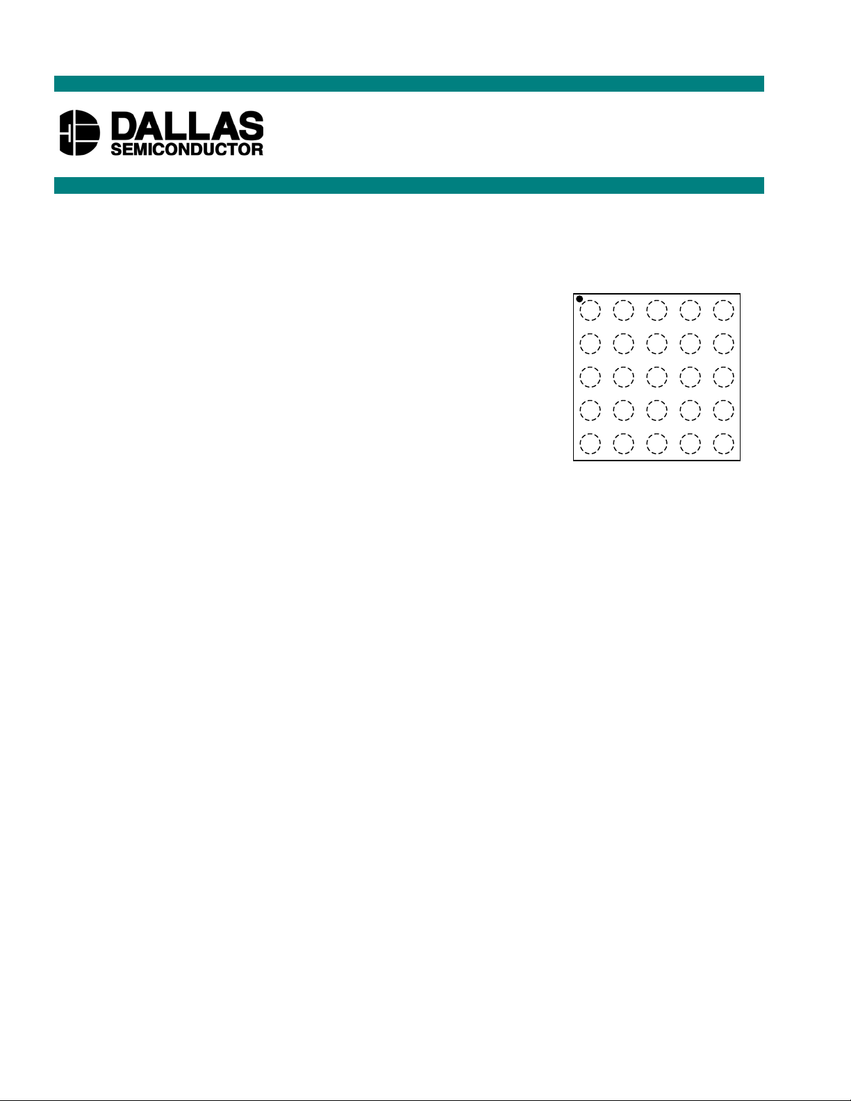
5 x 5 BGA (0.8mm pitch)
Top View
1 2 3 4 5
DS1852
ORDERING INFORMATION
DS1852B-000 25-BALL BGA
DESCRIPTION
The DS1852 transceiver monitor manages all system monitoring functions in a fiber optic data
transceiver module, in accordance with proposal SFF-8472. Its functions include 2-wire communications
with the host system, EEPROM memory for identification, tracking, and calibration, an ADC with four
muxing inputs, three fast comparators, and a temperature sensor to monitor an optical transceiver. The
DS1852 has programmable alarm and warning flags for all four analog-to-digital (A/D) conversion
values (three user analog inputs plus supply voltage) as well as the temperature. These conditions can be
used to determine critical parameters inside each module. The three fast comparators have temperaturecompensated programmability. The temperature dependencies of the trip points aid in assessing critical
conditions.
The DS1852 is offered for sale free of any royalty or licensing fees. However, users should be aware that implementation of the SFF-8472
proposed specifications may require the use of an invention covered by patent rights. Since these patents relate to the SFF-8472 specification
and not to the DS1852 itself, licensing questions should be directed to Finisar Corp.
1 of 25 040302
Page 2

DS1852
PIN DESCRIPTIONS
Name Ball Locations Description
VCC D2, D4, E3 Power-Supply Terminal. The DS1852 will support supply voltages
ranging from +2.7V to +5.5V.
GND B3, C2, C4, D3 Ground Terminal
SDA B5 2-Wire Serial Data. The serial data pin is for serial data transfer to and
from the DS1852. The pin is open drain and may be wire-OR’ed with
other open-drain or open-collector interfaces.
SCL A5 2-Wire Serial Clock. The serial clock input is used to clock data into
the DS1852 on rising edges and clock data out on falling edges.
B
A3 Analog Input Pin (Bias Value). Input to A/D.
in
Pin D1 Analog Input Pin (Lower Level). Input to A/D.
Rin A2 Analog Input Pin (Received Power). Input to A/D.
ASEL B2 Address Select Pin. If set to logic 0, the device address is A0h. If set to
logic 1, the value in Table 3, byte D0h determines the chip address
(factory default is A2h). For SFF-8472 compliance, this pin should be
connected high.
Din C5 Digital Input Pin (TX Disable). Digital input for mirroring in memory
map.
RSin B4 Digital Input Pin (Rate Select). Digital input for mirroring in memory
map.
E5 Digital Input Pin (TX Fault). Digital input for mirroring in memory
F
in
map.
L
A1 Digital Input Pin (LOS). Digital input for mirroring in memory map.
in
NC A4, B1, C1, D5, No Connect
E1, E2, E4, C3
2 of 25
Page 3
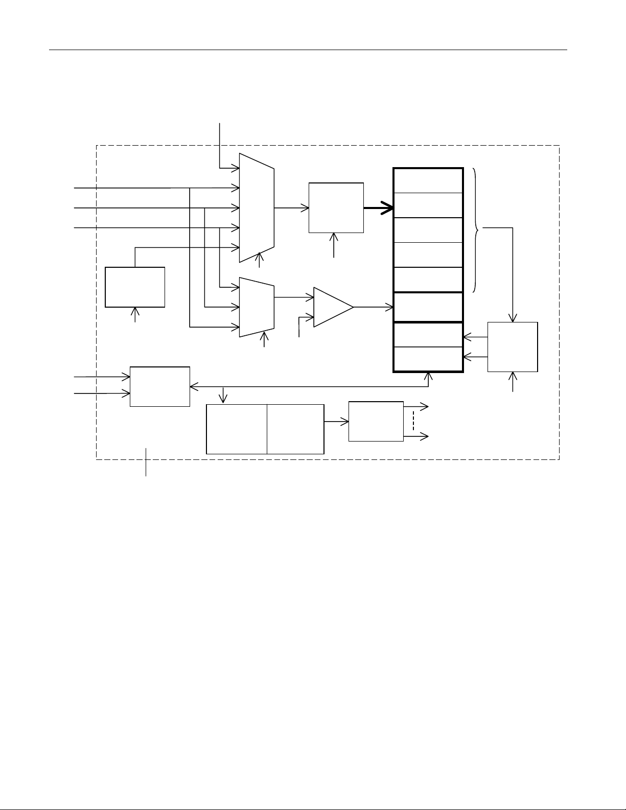
DS1852 BLOCK DIAGRAM Figure 1
V
CC
B
IN
P
R
IN
IN
5:1
MUX
ADC
DS1852
OUTPUT REGISTERS
V
B
SDA
SCL
TEMP
SENSOR
Control
2-WIRE
Interface
GND
Control
3:1
MUX
Control
EEPROM
CUSTOMER
EEPROM
Control
CONTROL
SETTINGS
Control
FAST
TRIP
CONTROL
LOGIC
P
R
FAST
ALARM
WARN
Control
Signals
ALARM
and
Control
3 of 25
Page 4

DS1852
DEVICE OPERATION
Security
To prevent accidental overwrites of key device data, a data lockout feature is incorporated. A 32-bit
password provides access to the “manufacturer” memory locations. These locations are in addition to the
unprotected “user” memory locations:
1) User—This is the default state after power-up; it allows read access to standard IEEE identity table
and standard monitoring and status functions.
2) Manufacturer Level 1—This allows access to customer data table and some selected setups (password
1).
3) Manufacturer Level 2—This allows access to all memory, settings, and features (password 2).
The level 1 password is located in Table 03h EEPROM (bytes D3h to D6h) and may be changed by
gaining access through the level 2 password.
The level 2 password is set in protected EEPROM and is programmed during factory test.
During power-up, the 32-bit password entry (addresses 7Bh to 7Eh) is set to all 1s. This is the value that
is compared to the level 1 password entry in Table 03h to grant level 1 access. Therefore, the level 1
password should not be set to all 1s or the user will gain level 1 access after each power-on.
By default, both passwords are factory preset to 00h.
To gain access to a security level, a 4-byte password is written into Table 00h, bytes 7Bh to 7Eh. If the
written data matches one of the passwords, that corresponding level of access is granted until the
password entry is changed or the power is cycled. Entering the level 2 password allows access to both
the level 1 data and the level 2 data. The 4-byte password is write-only.
4 of 25
Page 5
DS1852
ANALOG-TO-DIGITAL CONVERTER
The ADC reads a total of five inputs: VCC (internal), temperature (internal), and external inputs Bin, Pin,
and Rin. All conversions are updated every 13ms (nominal) or 20ms (max) in rotation. The conversions
are absolute and compared to an internal reference. While the 16-bit values are read, only the upper 12
are significant. The lower four bits are undefined.
The temperature and analog voltage inputs are calibrated by Dallas Semiconductor and read with the
following scale:
Temperature: High byte: -128°C to +127°C signed; low byte: 1/256°C. The lower four bits
should be ignored.
S2625242322212
2-12-22-32-42-52-62-72
0
-8
VCC: This reads as an unsigned 16-bit quantity at 100mV LSB, with a maximum range of
6.5535V, when using the factory default value. The lower four bits should be ignored.
Bin, P
: These read as an unsigned 16-bit quantity at 38.147mV LSB, with a maximum range
in, Rin
of 2.500V, when using factory default values. The lower four bits should be ignored.
215214213212211210292
272625242322212
8
0
Each analog input has a 16-bit scaling calibration in Table 03h EEPROM. This allows the analog
conversion values to be calibrated for full scale at any input voltage from 0.2V to 6.5535V. The ADC
conversion value will clamp rather than roll over. Each external analog channel has a maximum input
voltage of VCC independent of the calibration factor.
The upper four bits of scaling select the coarse range; the lower 12 bits are for fine adjustments. The
algorithm to trim the scale is described below.
The scaling factors for each input (VCC, VBin, VPin, and VRin) are 16 bits wide. They are located in
Table 03h at addresses C8h to CFh, respectively. The 16 bits are a combination of two trims. The lower
12 bits are binary weighted and give the high resolution trim for scaling the input to output relationship.
The upper four bits are a coarse-adjust of the lower 12 bits. In other words, the upper four bits scale the
LSB value of the binary weighted lower 12 bits.
As an illustration, assume a value of 1V is needed to read full scale. Force a voltage less than 1V
(975mV, for example) to keep clamping out of the way. The closer to max voltage the better, but not too
close.
1) Set the scale trim to 0FFFh (the upper four bits to all zeros and the lower 12 bits to all ones).
2) Use a SAR approach on the upper four bits, starting with 1000b, to find the smallest 4-bit trim
necessary to cause the voltage reading to be above the input (in this case, greater than or equal to
975mV). If they all clamp, that is okay. That means 0000b is the needed value for the upper four
5 of 25
Page 6

DS1852
bits. This step has now adjusted the LSB of the lower 12 bits so that the best possible trim is
acquired with the lower 12 bits.
If too high a value is used in the four bits, then the resolution of the 12 bits is too high and absolute
accuracy is sacrificed. If too low a value is used in the four bits, then the resolution of the 12 bits is too
small, so a maximum reading is not possible and a large gain error is present through the entire range.
Example code can be found near the end of this data sheet.
POWER-ON LOGIC
VCC is compared to an internal reference voltage, and if it is below VCC minimum, all internal logic and
outputs are held in their reset state. When VCC rises above VCC minimum, the system reset is released.
The DS1852 will not begin monitoring operations until VCC has risen above the analog minimum
voltage. However, communication on the 2-wire bus can occur at a V
minimum voltage. This allows access to the power-on logic bit located in Table 00h, address 6Eh, bit 0.
The analog minimum voltage is less than 2.7V but greater than the digital minimum voltage. Above the
analog minimum voltage, the DS1852 will begin to function in a predictable manner but will not satisfy
specifications until VCC is above 2.7V.
level lower than the analog
CC
TEMPERATURE-DEPENDENT FAST ALARM COMPARATORS
The DS1852 has a three-input muxing fast alarm comparator with a response time of less than 10µs for
each input. This provides a coarse but fast approximation of whether analog inputs Bin, P
and Rin are
in,
above their temperature-dependent value. Each comparator has an 8-bit max value set in Table 03h,
address D8h to E7h. The trip point range is adjustable from 10mV to 2.5V. Each LSB is approximately
10mV. The outputs of these comparators are readable in Table 00h (alarm bytes 1 and 0) and may be
overwritten if their corresponding fast alarm override bit is set in Table 03h EEPROM.
The Bin alarm can be set to eight unique temperature-dependent trip values, which allows the user to set
trip points for different temperature ranges. The Pin/Rin fast alarms act similarly, but can only be set to
four unique temperature-dependent values. For more information, refer to Table 03h.
HIGH-RESOLUTION ALARM COMPARATORS
There are 10 alarm comparators for the five analog channels. There is a 'high alarm' comparator whose
output is active if the analog signal is above its threshold and a 'low alarm' comparator whose output is
active if the analog signal is below its threshold. These comparators have a 2-byte set point in the same
format as the analog converter data in Table 03h. The outputs of these comparators are readable in Table
00h (70h) and may be overwritten if their corresponding alarm override bit is set in Table 03h
EEPROM.
WARNING COMPARATORS
The 10 warning comparators function the same way as the alarm comparators, but can be set to trip at
different levels. Typically, they would be set to trip prior to the alarm comparators. The set points are in
Table 03h and the outputs can be read from Table 00h.
6 of 25
Page 7

DS1852
DIGITAL INPUTS
The four digital inputs (Din, RSin, Fin, and Lin) can be read through the 2-wire bus. The logic levels at
these inputs are mirrored in the “logic states” byte (6Eh) in Table 00h.
2-WIRE OPERATION
Clock and Data Transitions
The SDA pin is normally pulled high with an external resistor or device. Data on the SDA pin may only
change during SCL low time periods. Data changes during SCL high periods will indicate a start or stop
conditions depending on the conditions discussed below. See Figure 2 for further details.
Start Condition
A high-to-low transition of SDA with SCL high is a start condition that must precede any other
command. See Figure 2 for further details.
Stop Condition
A low-to-high transition of SDA with SCL high is a stop condition. After a read sequence, the stop
command places the DS1852 into a low-power mode. See Figure 2 for further details.
Acknowledge Bit
All address bytes and data bytes are transmitted through a serial protocol. The DS1852 pulls SDA low
during the ninth clock pulse to acknowledge that it has received each word.
Standby Mode
The DS1852 features a low-power mode that is automatically enabled after power-on, after a stop
command, and after the completion of all internal operations.
2-Wire Interface Reset
After any interruption in protocol, power loss, or system reset, the following steps reset the DS1852:
1) Clock up to nine cycles.
2) Look for SDA high in each cycle while SCL is high.
3) Create a start condition while SDA is high.
Device Addressing
The DS1852 must receive an 8-bit device address word following a start condition to enable a specific
device for a read or write operation. The address word is clocked into the DS1852 MSB to LSB. The
address word defaults to A0h then the R/W (READ/WRITE) bit when ASEL is a logic zero. If the R/W
bit is high, a read operation is initiated. If R/W is low, a write operation is initiated. The device address
is changed to the internal chip address (Table 03h address D0h) when ASEL is logic one. The default
internal chip address from the factory is A2h.
7 of 25
Page 8

DS1852
Write Operations
After receiving a matching address byte with the R/W bit set low, the device goes into the write mode of
operation. The master must transmit an 8-bit EEPROM memory address to the device to define the
address where the data is to be written. After the byte has been received, the DS1852 will transmit a zero
for one clock cycle to acknowledge the receipt of the address. The master must then transmit an 8-bit
data word to be written into this address. The DS1852 will again transmit a zero for one clock cycle to
acknowledge the receipt of the data. At this point the master must terminate the write operation with a
stop condition for the write to be initiated. If a start condition is sent in place of the stop condition, the
write is aborted and the data received during that operation is discarded. If the stop condition is received,
the DS1852 enters an internally timed write process (tw) to the EEPROM memory. The DS1852 will not
send an acknowledge bit for any 2-wire communication during the EEPROM write process.
The DS1852 is capable of an 8-byte page write. A page is any 8-byte block of memory starting with an
address evenly divisible by eight and ending with the starting address plus seven. For example,
addresses 00h through 07h constitute one page. Other pages would be addresses 08h through 0Fh, 10h
through 17h, 18h through 1Fh, etc.
A page write is initiated the same way as a byte write, but the master does not send a stop condition after
the first byte. Instead, after the slave has received the data byte, the master can send up to seven more
bytes using the same nine-clock sequence. The master must terminate the write cycle with a stop
condition or the data clocked into the DS1852 will not be latched into permanent memory.
The address counter rolls on a page during a write. The counter does not count through the entire
address space as during a read. For example, if the starting address is 06h and four bytes are written, the
first byte goes into address 06h. The second goes into address 07h. The third goes into address 00h (not
08h). The fourth goes into address 01h. If more than nine or more bytes are written before a stop
condition is sent, the first bytes sent are overwritten. Only the last eight bytes of data are written to the
page.
Acknowledge Polling
Once the internally timed write has started and the DS1852 inputs are disabled, acknowledge polling can
be initiated. The process involves transmitting a start condition followed by the device address. The
R/W bit signifies the type of operation that is desired. The read or write sequence will only be allowed to
proceed if the internal write cycle has completed and the DS1852 responds with a zero.
Read Operations
After receiving a matching address byte with the R/W bit set high, the device goes into the read mode of
operation. There are three read operations: current address read, random read, and sequential address
read.
CURRENT ADDRESS READ
The DS1852 has an internal address register that contains the address used during the last read or write
operation, incremented by one. This data is maintained as long as VCC is valid. If the most recent address
was the last byte in memory, then the register resets to the first address. This address stays valid between
operations as long as power is available.
8 of 25
Page 9

DS1852
Once the device address is clocked in and acknowledged by the DS1852 with the R/W bit set to high,
the current address data word is clocked out. The master does not respond with a zero, but does generate
a stop condition afterwards.
RANDOM READ
A random read requires a dummy byte write sequence to load in the data word address. Once the device
and data address bytes are clocked in by the master, and acknowledged by the DS1852, the master must
generate another start condition. The master now initiates a current address read by sending the device
address with the R/W bit set high. The DS1852 will acknowledge the device address and serially clocks
out the data byte.
SEQUENTIAL ADDRESS READ
Sequential reads are initiated by either a current address read or a random address read. After the master
receives the first data byte, the master responds with an acknowledge. As long as the DS1852 receives
this acknowledge after a byte is read, the master may clock out additional data words from the DS1852.
After reaching address FFh, it resets to address 00h.
The sequential read operation is terminated when the master initiates a stop condition. The master does
not respond with a zero.
For a more detailed description of 2-wire theory of operation, see 2-WIRE SERIAL PORT OPERATION.
9 of 25
Page 10

DS1852
2-WIRE SERIAL PORT OPERATION
The 2-wire serial port interface supports a bidirectional data transmission protocol with device
addressing. A device that sends data on the bus is defined as a transmitter, and a device receiving data as
a receiver. The device that controls the message is called a “master.” The devices that are controlled by
the master are “slaves”. A master device that generates the serial clock (SCL), controls the bus access,
and generates the START and STOP conditions must control the bus. The DS1852 operates as a slave
on the 2-wire bus. Connections to the bus are made through the open-drain I/O lines SDA and SCL. The
following I/O terminals control the 2-wire serial port: SDA, SCL, and ASEL. Timing diagrams for the
2-wire serial port can be found in Figures 2 and 3. Timing information for the 2-wire serial port is
provided in the AC ELECTRICAL CHARACTERISTICS table for 2-wire serial communications.
The following bus protocol has been defined:
§ Data transfer may be initiated only when the bus is not busy.
§ During data transfer, the data line must remain stable whenever the clock line is HIGH. Changes in
the data line while the clock line is HIGH will be interpreted as control signals.
Accordingly, the following bus conditions have been defined:
Bus not busy: Both data and clock lines remain HIGH.
Start data transfer: A change in the state of the data line from HIGH to LOW while the clock is HIGH
defines a START condition.
Stop data transfer: A change in the state of the data line from LOW to HIGH while the clock line is
HIGH defines the STOP condition.
Data valid: The state of the data line represents valid data when, after a START condition, the data line
is stable for the duration of the HIGH period of the clock signal. The data on the line can be changed
during the LOW period of the clock signal. There is one clock pulse per bit of data. Figures 2 and 3
detail how data transfer is accomplished on the 2-wire bus. Depending upon the state of the R/W bit, two
types of data transfer are possible.
Each data transfer is initiated with a START condition and terminated with a STOP condition. The
number of data bytes transferred between START and STOP conditions is not limited and is determined
by the master device. The information is transferred byte-wise and each receiver acknowledges with a
ninth bit.
Within the bus specifications a regular mode (100kHz clock rate) and a fast mode (400kHz clock rate)
are defined. The DS1852 works in both modes.
Acknowledge: Each receiving device, when addressed, is obliged to generate an ‘acknowledge’ after
the byte has been received. The master device must generate an extra clock pulse, which is associated
with this acknowledge bit.
10 of 25
Page 11

DS1852
A device that acknowledges must pull down the SDA line during the acknowledge clock pulse in such a
way that the SDA line is a stable LOW during the HIGH period of the acknowledge-related clock pulse.
Of course, setup and hold times must be taken into account. A master must signal an end of data to the
slave by not generating an acknowledge bit on the last byte that has been clocked out of the slave. In this
case, the slave must leave the data line HIGH to enable the master to generate the STOP condition.
1) Data transfer from a master transmitter to a slave receiver. The first byte transmitted by the master is
the command/control byte. Next follows a number of data bytes. The slave returns an acknowledge
bit after each received byte.
2) Data transfer from a slave transmitter to a master receiver. The master transmits the first byte (the
command/control byte) to the slave. The slave then returns an acknowledge bit. Next follows a
number of data bytes transmitted by the slave to the master. The master returns an acknowledge bit
after all received bytes other than the last byte. At the end of the last received byte, a ‘not
acknowledge’ can be returned.
The master device generates all serial clock pulses and the START and STOP conditions. A transfer is
ended with a STOP condition or with a repeated START condition. Since a repeated START condition
is also the beginning of the next serial transfer, the bus will not be released.
The DS1852 may operate in the following two modes:
1) Slave receiver mode: Serial data and clock are received through SDA and SCL, respectively. After
each byte is received, an acknowledge bit is transmitted. START and STOP conditions are
recognized as the beginning and end of a serial transfer. Address recognition is performed by
hardware after reception of the slave (device) address and direction bit.
2) Slave transmitter mode: The first byte is received and handled as in the slave receiver mode.
However, in this mode the direction bit will indicate that the transfer direction is reversed. Serial
data is transmitted on SDA by the DS1852 while the serial clock is input on SCL. START and STOP
conditions are recognized as the beginning and end of a serial transfer.
Slave Address: Command/control byte is the first byte received following the START condition from
the master device. The command/control byte consists of a 4-bit control code. For the DS1852, this is set
as 1010 000 (when ASEL is ‘0’) binary for R/W operations. The last bit of the command/control byte
(R/W) defines the operation to be performed. When set to a 1 a read operation is selected, and when set
to a 0 a write operation is selected.
Following the START condition, the DS1852 monitors the SDA bus checking the device type identifier
being transmitted. Upon receiving the chip address control code, and the R/W bit, the slave device
outputs an acknowledge signal on the SDA line.
11 of 25
Page 12

2-WIRE DATA TRANSFER PROTOCOL Figure 2
DS1852
2-WIRE AC CHARACTERISTICS Figure 3
12 of 25
Page 13

DS1852
MEMORY MAP
Memory access to the DS1852 is through the 2-wire interface. See the 2-WIRE OPERATION section.
The memory within the DS1852 is organized into multiple tables. The lower 128 bytes of memory are
common to all tables, the upper 128 bytes are addressed according to the table select byte at 7Fh. Valid
values of the table address byte are 00h to 03h, to access Tables 00h through 03h.
00h
Tables 00h –
03h
Lower
128 bytes
R- All
W - Level 2*
7Fh
80h
Table 00h
Upper
128 Bytes
No Physical
Memory
FF FF FF
*For permission details of this memory block refer to following table.
Table 01h
Upper
128 Bytes
R/W - Level 1
FF
80h80h
Table 02h
Upper
128 Bytes
R/W - Level 2
80h
Table 03h
Upper
128 Bytes
R/W - Level 2
The following tables detail the memory contents. Where descriptions are underlined an expanded table
indicates the function of individual bits within the byte. The reserved memory locations should not be
used even though R/W access may be possible.
Not all memory is EEPROM; RAM cells are shaded within the tables, and denoted beneath.
13 of 25
Page 14

DS1852
Table 00h-FFh (Lower)
Address Byte 0 Byte 1 Byte 2 Byte 3 Byte 4 Byte 5 Byte 6 Byte 7
bits<7-0> bits<7-0> bits<7-0> bits<7-0> bits<7-0> bits<7-0> bits<7-0> bits<7-0>
00h
…
…
(Read Access – All, Write Access – Level 2)
IEEE Data EEPROM
58h
60h Temp MSB Temp LSB Vcc MSB Vcc LSB Bin MSB B
LSB Pin MSB Pin LSB
in
68h Rin MSB Rin LSB reserved reserved reserved reserved I/O states AD updated
70h Alarm flag3 alarm flag2 alarm flag1 alarm flag0 warn flag3 warn flag2 warn flag1 warn flag0
78h Reserved reserved reserved PWE Byte 3 PWE Byte 2 PWE Byte 1 PWE Byte 0 table select
Bytes 60h through 7Fh are RAM, see expanded table for access requirements.
Table 00h-FFh (Lower) Expanded
Byte Name Bit 7 Bit 6 Bit 5 Bit 4 Bit 3 Bit 2 Bit 1 Bit 0
I/O states (1) D
AD updated
(2)
T-updated V-updated B-updated P-updated R-updated reserved reserved reserved
in
reserved reserved RS
in
reserved F
in
L
in
power-on logic
alarm flag3 (3) T-ad hi T-ad lo V-ad hi V-ad lo B-ad hi B-ad lo P-ad hi P-ad lo
alarm flag2 (3) R-ad hi R-ad lo reserved reserved reserved reserved reserved reserved
alarm flag1 (3) reserved reserved reserved reserved B-ft hi reserved P-ft hi reserved
alarm flag0 (3) R-ft hi reserved reserved reserved reserved reserved reserved reserved
warn flag3 (3) T-ad hi T-ad lo V-ad hi V-ad lo B-ad hi B-ad lo P-ad hi P-ad lo
warn flag2 (3) R-ad hi R-ad lo reserved reserved reserved reserved reserved reserved
warn flag1 (3) reserved reserved reserved reserved reserved reserved reserved reserved
warn flag0 (3) reserved reserved reserved reserved reserved reserved reserved reserved
(1) Read Access – All, Write Access – None
(2) Read Access – All, Write Access – All (The DS1852 will also write to this byte)
(3) Read Access – All, Write Access – Level 2 + config bit (Table 03h, E8h)
14 of 25
Page 15

DS1852
Table 00h (Lower)
Memory Location
Name of Location Function
(Table 00h, Lower)
00h – 5Fh IEEE Data This memory block is used to store required GBIC data.
60h Temperature MSB This byte contains the MSB of the 15-bit 2’s complement
temperature output from the temperature sensor.
61h Temperature LSB This byte contains the LSB of the 15-bit 2’s complement
temperature output from the temperature sensor.
62h – 63h Vcc Value These bytes contain the MSB (62h) and the LSB (63h) of the
measured V
CC
.
64h – 65h Bin Value These bytes contain the MSB (64h) and the LSB (65h) of the
measured B
in.
66h – 67h Pin Value These bytes contain the MSB (66h) and the LSB (67h) of the
measured P
in.
68h – 69h Rin Value These bytes contain the MSB (68h) and the LSB (69h) of the
measured R
in.
6Eh IO States Bit 0 will be 0 when the analog monitoring is active.
6Fh A/D Updated Allows the user to verify if an update from the A/D has occurred to
the five values: temperature, V
, Bin, Pin and Rin. The user writes
CC
the byte to 00h. Once a conversion is complete for a given value, its
bit will change to ‘1’.
70h – 73h Alarm Flags These bits reflect the state of the alarms as a conversion updates.
High alarm bits are ‘1’ if converted value is greater than
corresponding high limit. Low alarm bits are ‘1’ if converted value
is less than corresponding low limit. Otherwise, bits are ‘0’.
74h – 77h Warning Flags These bits reflect the state of the warnings as a conversion updates.
High warning bits are ‘1’ if converted value is greater than
corresponding high limit. Low warning bits are ‘1’ if converted
value is less than corresponding low limit. Otherwise, bits are ‘0’.
7Bh – 7Eh Password Entry Bytes
PWE Byte 3 (7Bh) MSByte
PWE Byte 2 (7Ch)
The four bytes are used for password entry. The entered password
will determine the user’s R/W privileges. During power-up these
bits are set to all 1s.
PWE Byte 1 (7Dh)
PWE Byte 0 (7Eh) LSByte
7Fh Table Select Byte This byte determines which of the upper memory pages are
selected.
00h — No physical memory
01h — Manufacturer EEPROM
02h — Manufacturer EEPROM
03h — Device settings
15 of 25
Page 16

DS1852
Table 00h (Upper)
Address
80h
…
…
F8h
Address
80h
…
…
F0h
F8h reserved
Byte 0 Byte 1 Byte 2 Byte 3 Byte 4 Byte 5 Byte 6 Byte 7
bits<7-0> bits<7-0> bits<7-0> bits<7-0> bits<7-0> bits<7-0> bits<7-0> bits<7-0>
Reserved by IEEE
(no physical memory)
Table 01h (Upper)
Byte 0 Byte 1 Byte 2 Byte 3 Byte 4 Byte 5 Byte 6 Byte 7
bits<7-0> bits<7-0> bits<7-0> bits<7-0> bits<7-0> bits<7-0> bits<7-0> bits<7-0>
Manufacturer EEPROM
(Read Access – Level 1, Write Access – Level 1)
Address FFh is RAM
Address
80h
…
…
F8h
Byte 0 Byte 1 Byte 2 Byte 3 Byte 4 Byte 5 Byte 6 Byte 7
bits<7-0> bits<7-0> bits<7-0> bits<7-0> bits<7-0> bits<7-0> bits<7-0> bits<7-0>
Table 02h (Upper)
Manufacturer EEPROM
(Read Access – Level 2, Write Access – Level 2)
16 of 25
Page 17

DS1852
Table 03h (Upper)
Address Byte 0 Byte 1 Byte 2 Byte 3 Byte 4 Byte 5 Byte 6 Byte 7
bits<7-0> bits<7-0> bits<7-0> bits<7-0> bits<7-0> bits<7-0> bits<7-0> bits<7-0>
HI ALARM LO ALARM HI WARN LO WARN
80h T alarm MSB T alarm LSB T alarm MSB T alarm LSB T warn MSB T warn LSB T warn MSB T warn LSB
88h V alarm MSB V alarm LSB V alarm MSB V alarm LSB V warn MSB V warn LSB V warn MSB V warn LSB
90h B alarm MSB B alarm LSB B alarm MSB B alarm LSB B warn MSB B warn LSB B warn MSB B warn LSB
98h P alarm MSB P alarm LSB P alarm MSB P alarm LSB P warn MSB P warn LSB P warn MSB P warn LSB
A0h R alarm MSB R alarm LSB R alarm MSB R alarm LSB R warn MSB R warn LSB R warn MSB R warn LSB
A8h reserved reserved reserved reserved reserved reserved reserved reserved
B0h reserved reserved reserved reserved reserved reserved reserved reserved
B8h reserved reserved reserved reserved reserved reserved reserved reserved
C0h reserved reserved reserved reserved reserved reserved reserved reserved
C8h
V-ad scale MSB V-ad scale LSB B-ad scale MSB B-ad scale LSB P-ad scale MSB P-ad scale LSB R-ad scale MSB R-ad scale LSB
D0h chip address reserved reserved PW1 Byte 3 PW1 Byte 2 PW1 Byte 1 PW1 Byte 0 reserved
D8h B Fast trip0 B Fast trip1 B Fast trip2 B Fast trip3 B Fast trip4 B Fast trip5 B Fast trip6 B Fast trip7
E0h P Fast trip0 P Fast trip1 P Fast trip2 P Fast trip3 R Fast trip0 R Fast trip1 R Fast trip2 R Fast trip3
E8h config/o-ride reserved reserved reserved reserved reserved reserved reserved
F0h reserved reserved reserved reserved reserved reserved reserved reserved
F8h reserved reserved reserved reserved reserved reserved reserved reserved
Address E8h is RAM.
Read Access – Level 2, Write Access – Level 2
Fast-Trip Temperature Relationships
Fast Trip
Byte 0 Byte 1 Byte 2 Byte 3 Byte 4 Byte 5 Byte 6 Byte 7
bits<7-0> bits<7-0> bits<7-0> bits<7-0> bits<7-0> bits<7-0> bits<7-0> bits<7-0>
* B-in
* P-in
* R-in
< –8
< 8
< 8
[-8 to 8) [8 to 24) [24 to 40) [40 to 56) [56 to 72) [72 to 88)
[8 to 40) [40 to 72)
[8 to 40) [40 to 72)
³ 72
³ 72
* There is one degree of hysteresis at transitions only (e.g., for B-in, if temp increases to +8.0°C then byte 2 is active. It will
remain active until temp reaches +24.0°C or falls below +7.0°C.).
Table 03h (Expanded)
Byte Name
Chip address
X-ad scale
MSB*
X-ad scale
LSB*
config/O-ride
Bit 7 Bit 6 Bit 5 Bit 4 Bit 3 Bit 2 Bit 1 Bit 0
7
b
15
2
7
2
reserved reserved manual AD
6
b
14
2
6
2
5
b
13
2
5
2
4
b
12
2
4
2
3
b
11
2
3
2
2
b
10
2
2
2
1
b
9
2
1
2
EE Bar SW-POR A/D Enable Manual fast
alarm
alarm
³ 88
X
8
2
0
2
reserved
* V-, B-, P- or R- as appropriate
17 of 25
Page 18

DS1852
Table 03h
Memory Location
Name of Location Function of Location
(Table 3)
80h – 81h
88h – 89h
90h – 91h
98h – 99h
A0h – A1h
82h – 83h
8Ah – 8Bh
92h – 93h
9Ah – 9Bh
A2h – A3h
84h – 85h
8Ch – 8Dh
94h – 95h
9Ch – 9Dh
A4h – A5h
86h – 87h
8Eh – 8Fh
96h – 97h
9Eh – 9Fh
A6h – A7h
Temperature High Alarm
V
High Alarm
CC
B
High Alarm
in
P
High Alarm
in
R
High Alarm
in
Temperature Low Alarm
V
Low Alarm
CC
Low Alarm
B
in
P
Low Alarm
in
R
Low Alarm
in
Temp High Warning
V
High Warning
CC
B
High Warning
in
P
High Warning
in
High Warning
R
in
Temperature Low Warning
V
Low Warning
CC
B
Low Warning
in
P
Low Warning
in
R
Low Warning
in
The value written to this location serves as the high alarm limit. Data
format is the same as the corresponding value (temperature, V
P
, Rin).
in
CC
, Bin,
The value written to this location serves as the low alarm limit. Data
format is the same as the corresponding value (temperature, V
, Rin).
P
in
CC
, Bin,
The value written to this location serves as the high warning limit.
Data format is the same as the corresponding value (temperature,
V
, Bin, Pin, Rin).
CC
The value written to this location serves as the low warning limit.
Data format is the same as the corresponding value (temperature,
V
, Bin, Pin, Rin).
CC
B2h, Bah, C5h – C7h Logic State Control These should be left at the factory default values as shown in the
table to allow reading of the digital inputs from address 6Eh in Table
00h.
C8h – C9h
CAh – CBh
CCh – CDh
CEh - CFh
V
– A/D Scale
CC
B
– A/D Scale
in
P
– A/D Scale
in
R
– A/D Scale
in
16 bits of gain adjustment for corresponding A/D conversion values.
D0h Chip Address This is the chip address used when pin ASEL is high (A2h default).
D3h – D6h PW1 Byte 3 (D3h) MSB
PW1 Byte 2 (D4h)
The four bytes are used for password 1 entry. The password entered
here will allow Level 1 access. Factory default is 00h.
PW1 Byte 1 (D5h)
PW1 Byte 0 (D6h) LSB
D8h – DFh Bin Fast Trip These bytes define the fast-trip comparison over temperature.
E0h – E3h Pin Fast Trip These bytes define the fast-trip comparison over temperature.
E4h – E7h Rin Fast Trip These bytes define the fast-trip comparison over temperature.
E8h Configuration Override
Location of the bits is defined in Table 03h expanded.
Byte
18 of 25
Page 19

DS1852
ABSOLUTE MAXIMUM RATINGS*
Voltage on Any Pin Relative to Ground -0.3V to +6.0V
Operating Temperature Range -40°C to +125°C
Programming Temperature Range 0°C to +70°C
Storage Temperature Range -55°C to +125°C
Soldering Temperature See J-STD-020A specification
*This is a stress rating only and functional operation of the device at these or any other conditions
above those indicated in the operation sections of this specification is not implied. Exposure to
absolute maximum rating conditions for extended periods of time may affect reliability.
RECOMMENDED DC OPERATING CONDITIONS (-40°C to +100°C)
PARAMETER SYMBOL MIN TYP MAX UNITS NOTES
Supply Voltage V
CC
+2.7 +5.5 V 1
DC ELECTRICAL CHARACTERISTICS (-40°C to +100°C; VCC = 2.7V to 5.5V)
PARAMETER SYMBOL CONDITIONS MIN TYP MAX UNITS NOTES
Supply Current I
Digital Power-On
RESET
Analog Power-On
RESET
Input Leakage (SDA,
SCL)
Input Logic 1 (SDA,
SCL, ASEL)
Input Logic 0 (SDA,
SCL, ASEL)
Input Logic 1 (RSin,
Din, Fin, Lin)
Input Logic 0 (RSin,
Din, Fin, Lin)
V
V
V
V
V
V
I
CC
pod
poa
IL
IH
IL
IH
IL
2.0 2.5 V
-1 +1
0.7V
CC
GND -
0.3
1.5
GND -
0.3
1.0 mA 4
2.0 V
mA
VCC +
0.3
0.3
V
CC
VCC +
0.3
V
V
V
0.9 V
12
Current (SDA)
I/O Capacitance C
Input Resistance (RSin,
Din, Fin, Lin)
Input Resistance
(ASEL)
I
I
R
R
OL1
OL2
I/O
ipu
ipd
0.4V 3 mALow Level Output
0.6V 6 mA
10 pF
to V
CC
25 40 55
to GND 25 40 55
19 of 25
kW
kW
Page 20

DS1852
A/D CONVERTERS (-40°C to +100°C; VCC = 2.7V to 5.5V)
PARAMETER SYMBOL CONDITIONS MIN MAX UNITS NOTES
Thermometer Error T
Conversion Time t
ERR
CONVT
Voltage A/D input VAD
Voltage A/D Offset VAD
Absolute Voltage A/D
Error
Differential Voltage A/D
Nonlinearity
VAD
VAD
in
off
err
DNL
-40°C to +100°C
± 3.0 °C
12-bit conversion 10 20 ms
+
V
0.0
CC
0.3
± 0.25
± 0.5
± 0.25
V
% FSR
% FSR
% FSR
3
COMPARATORS (-40°C to +100°C; VCC = 2.7V to 5.5V)
PARAMETER SYMBOL CONDITIONS MIN MAX UNITS NOTES
Sample Time t
Fast-Trip Input Range FT
samp
range
810µs 2
0
VCC +
0.3
V
Fast-Trip Absolute Error FT
Fast-Trip Nonlinearity FT
err
DNL
±1.0
±2.0
% FSR
LSB
20 of 25
Page 21

DS1852
AC ELECTRICAL CHARACTERISTICS (-40°C to +100°C, V
= 2.7V to 5.5V)
CC
PARAMETER SYMBOL CONDITIONS MIN TYP MAX UNITS NOTES
SCL Clock
Frequency
Bus Free Time
Between STOP and
f
SCL
t
BUF
Fast Mode
Standard Mode
Fast Mode
Standard Mode
0
0
1.3
4.7
400
100
kHz 7
µs 7
START Condition
Hold Time
(Repeated)
t
HD:STA
Fast Mode
Standard Mode
0.6
4.0
µs 7, 8
START Condition
Low Period of SCL
Clock
High Period of SCL
Clock
Data Hold Time t
Data Setup Time t
Start Setup Time t
Rise Time of Both
SDA and SCL
t
LOW
t
HIGH
HD:DAT
SU:DAT
SU:STA
t
R
Fast Mode
Standard Mode
Fast Mode
Standard Mode
Fast Mode
Standard Mode
Fast Mode
Standard Mode
Fast Mode
Standard Mode
Fast Mode
Standard Mode
1.3
4.7
0.6
4.0
0
0
100
250
0.6
4.7
20+0.1C
µs 7
µs 7
0.9 µs 7, 9, 10
ns 7
µs 7
300
B
1000
ns 11
Signals
Fall Time of Both
SDA and SCL
t
F
Fast Mode
Standard Mode
20+0.1C
300
B
300
ns 11
Signals
Setup Time for STOP
Condition
Capacitive Load for
t
SU:STO
C
B
Fast Mode
Standard Mode
0.6
4.0
µs
400 pF 11
Each Bus Line
Startup Time t
ST
2ms 5
VCC Power-Up Rate 1 V/s
EEPROM Write
t
W
10 20 ms 6
Time
NONVOLATILE MEMORY CHARACTERISTICS
PARAMETER SYMBOL CONDITIONS MIN TYP MAX UNITS NOTES
Writes +85°C 50,000
21 of 25
Page 22

DS1852
NOTES
1) All voltages are referenced to ground.
2) This is the time for one comparison. The complete cycle is this value multiplied by 3.
3) Absolute voltage error for Bin, Pin, and Rin are valid from 0% to 98%.
4) ASEL = GND, SDA = SCL = Din = Fin = Lin = RSin = VCC.
5) The time to begin monitoring operations after VCC has risen above the analog minimum voltage.
6) After STOP command has been received. No acknowledges will be issued during this interval.
7) A fast mode device can be used in a standard mode system, but the requirement t
then be met. This will automatically be the case if the device does not stretch the low period of the
SCL signal. If such a device does stretch the low period of the SCL signal, it must output the next
data bit to the SDA line t
RMAX
+ t
= 1000 + 250 = 1250ns before the SCL line is released.
SU:DAT
8) After this period, the first clock pulse is generated.
9) The maximum t
HD:DAT
has only to be met if the device does not stretch the low period (t
SCL signal.
10) A device must internally provide a hold time of at least 300ns for the SDA signal (see the V
the SCL signal) in order to bridge the undefined region of the falling edge of SCL.
11) CB— total capacitance of one bus line in picofarads, timing referenced to 0.9VCC and 0.1VCC.
12) Input levels equal either VCC or GND.
> 250ns must
SU:DAT
LOW
) of the
IH MIN
of
22 of 25
Page 23

DS1852
SCALING THE ADC
procedure writeTrimValue(trim :integer); (* write trim to part *)
procedure forceReference(Vin: real); (* applies reference voltage to input pin*)
procedure waitForNewConversion(); (* writes update byte to zero and waits for update
of new conversion with present trim *)
function readValue():integer; (* reads converted digital answer *)
procedure ProgramTrim(trim :integer);(*enables EE for table3 & programs trim*)
Procedure calVad(maxInput :real)
var
Bit :integer; (* counter - represents bininary bit 15-0*)
trim :integer; (* present trim values *)
lsb :real; (* the lsb value of the voltage reading *)
Vin :real; (* the reference input voltage *)
Dec_in :integer; (* decimal representation of voltage input *)
Dec_out :integer; (* voltage reading in decimal *)
delta :integer; (* present error of voltage reading *)
bestDelta :integer; (* the error closest to zero *)
bestTrim :integer; (* the trim that gave the best delta *)
Begin
bestDelta := 1000000;
bestTrim := 0;
trim := 4095; (* 0FFFh *)
lsb := maxInput / 65535;
Dec_in := 63888; (* input is ~97.5% of full scale *)
Vin := lsb * Dec_in;
forceReference(Vin);
(*Use SAR approach to trim course adjust on VAD scale bits 15-12*)
for Bit := 15 downto 11 do (* must go 1 bit too far so that zero is
possible solution *)
begin
if (Bit > 11) then
begin
trim := trim + lshft(1,Bit);
end;
writeTrimValue(trim);
waitForNewConversion;
Dec_out := readVoltage;
delta := Dec_out - Dec_in;
if ( delta >= 0 ) then
23 of 25
Page 24

begin
bestTrim := trim;
if (Bit > 11) then
Begin
trim := trim - lshft(1,trimBit);
end;
end;
end;
(* The upper 4 bits of bestTrim contains the answer for the course adjustment.*)
(* It is the smallest value that allows full scale trim with the lower 12 bits*)
(* zero out the lower 12 bits of bestTrim *)
trim := land(bestTrim,61440(*F000h*)); (*land() is logical AND function*)
(*Use SAR approach to trim resolution on VAD scale bits 11-0*)
for Bit := 11 downto -1 do (* must go 1 bit too far so that zero is
possible solution *)
begin
if (Bit > 0) then
begin
trim := trim + lshft(1,Bit);
end;
DS1852
writeTrimValue(trim);
waitForNewConversion;
Dec_out := readVoltage;
delta := Dec_out - Dec_in;
if ( abs(delta) <= abs(bestDelta) ) then
begin
bestTrim := trim;
bestDelta := delta;
end;
if ( delta > 0 ) then
begin
if (Bit > 0) then
Begin
trim := trim - lshft(1,trimBit);
end;
end;
end;
(* bestTrim now contains the trim that gives the lowest delta*)
ProgramTrim(bestTrim);
end;
24 of 25
Page 25

MECHANICAL DRAWING
DS1852
25 of 25
 Loading...