

Page 1
General Description
The DS1843 is a sample-and-hold circuit useful for capturing fast signals where board space is constrained. It
includes a differential, high-speed switched capacitor
input sample stage, offset nulling circuitry, and an output buffer. The DS1843 is optimized for use in optical
line transmission (OLT) systems for burst-mode RSSI
measurement in conjunction with an external sense
resistor.
Applications
Gigabit Passive Optical Network (GPON) OLT
Gigabit Ethernet Passive Optical Network (GEPON) OLT
GPON Optical Network Unit
Sample and Hold
Features
♦ Fast Sample Time < 300ns
♦ Hold Time > 100µs
♦ Low Input Offset
♦ Buffered Output
♦ Small, 8-Pin µDFN (2mm x 2mm) Pb-Free Package
DS1843
Fast Sample-and-Hold Circuit
________________________________________________________________
Maxim Integrated Products
1
Ordering Information
V
OUTN
MAIN MEMORY
EEPROM/SRAM
A/D CONFIG/RESULTS,
SYSTEM STATUS BITS,
ALARMS/WARNINGS,
LOOKUP TABLES,
USER MEMORY
CONTROLLER
V
INP
V
CC
V
INN
SEN
GND
V
OUTP
V
CC
DEN
SDA
SCL
MON1
BIAS
DAC
12-BIT
ADC
MOD
DAC
BMD
SEN
STROBE
STROBE
MON4
MON3P
MON3N
ANALOG MUX
3.3V
3.3V
TEMP
SENSOR
I
2
C
INTERFACE
DS1843
DS1842/
MAX4007
R
IN
C
S
C
S
C
IN
C
IN
CONTROL
LOGIC
Typical Operating Circuit
19-4539; Rev 0; 5/09
For pricing, delivery, and ordering information, please contact Maxim Direct at 1-888-629-4642,
or visit Maxim’s website at www.maxim-ic.com.
+
Denotes a lead(Pb)-free/RoHS-compliant package.
TRL = Tape and reel.
PART TEMP RANGE PIN-PACKAGE
DS1843D+ -40°C to +85°C 8 μDFN
DS1843D+TRL -40°C to +85°C 8 μDFN
Pin Configuration appears at end of data sheet.
Page 2
DS1843
Fast Sample-and-Hold Circuit
2 _______________________________________________________________________________________
ABSOLUTE MAXIMUM RATINGS
RECOMMENDED OPERATING CONDITIONS
(TA= -40°C to +85°C, unless otherwise noted.)
Stresses beyond those listed under “Absolute Maximum Ratings” may cause permanent damage to the device. These are stress ratings only, and functional
operation of the device at these or any other conditions beyond those indicated in the operational sections of the specifications is not implied. Exposure to
absolute maximum rating conditions for extended periods may affect device reliability.
Voltage Range on VCC.............................................-0.5V to +6V
Voltage Range on V
OUTP
, V
OUTN
,
V
INP
, V
INN
, SEN, DEN ............................-0.5V to (VCC+ 0.5V)*
Operating Temperature Range ...........................-40°C to +85°C
Storage Temperature Range .............................-55°C to +125°C
Soldering Temperature ..............................................Refer to the
IPC/JEDEC J-STD-020 Specification.
DC ELECTRICAL CHARACTERISTICS
(V
CC
= +2.97V to +5.5V, TA= -40°C to +85°C, unless otherwise noted.)
*
Subject to not exceeding +6V.
Supply Voltage V
PARAMETER SYMBOL CONDITIONS MIN TYP MAX UNITS
CC
(Note 1) +2.97 +5.5 V
Supply Current ICC (Note 1) 5.7 9 mA
Input Capacitance C
Sample Capacitance C
Logic-Input Low V
Logic-Input High V
Input Leakage I
Input Voltage V
Output Voltage V
Output Impedance R
Output Capacitiv e Load C
Total Input Referenced Voltage
Offset: D ifferential
Total Input Referenced Voltage
Offset: S ingle-Ended
PARAMETER S YMBOL CONDITIONS MIN TYP MAX UNITS
All pins (Note 2) 7 pF
IN
V
S
IL
IH
IN
IN
OUT
OUTMAX
OUT
V
OS-DIFF
V
OS-SE
and V
INN
INP
SEN and DEN inputs
SEN and DEN inputs
V
or V
INN
INP,
VIN = V
V
OUT
= V
INP
- V
OUTP
each output pin
(Note 2) 1 1.3 k
Capacitance for stable operation 50 pF
V
= 2.9V, 1μs sample time, VIN = 6mV 3.6 6.1 mV
CC
Voltco (V
V
Voltco (V
CC
= 2.9V, 1μs sample time, VIN = 6mV 3.4 8 mV
CC
CC
(Note 2) 5 pF
0.3 x
V
CC
0.7 x
V
CC
V
SEN = 0 1 μA
0 1.0 V
INN
- V
; 100k load on
OUTN
0 1.0 V
= 2.9V to 5.5V) 1 mV/V
= 2.9V to 5.5V) 1 mV/V
V
Page 3
DS1843
Fast Sample-and-Hold Circuit
_______________________________________________________________________________________ 3
Note 1: All voltages are referenced to ground. Currents entering the IC are specified positive and currents exiting the IC are negative.
Note 2: Guaranteed by design.
Note 3: V
OUT
at the end of the 10μs hold time is within specified % of VINduring the sample window; a 2.5kΩ resistor connected in
series to both V
INP
and V
INN(VINP
- V
INN
= 1V). External capacitance to ground for both V
INP
and V
INN
is approximately 10pF.
Note 4: The sampling capacitor must be removed from the input signal before the input signal changes. Therefore, the SEN pin
must be low for a short period of time, t
DEL
, before the input changes.
Note 5: V
OUT
at the end of the hold time is within 1% of VINduring the sample window (V
INP
- V
INN
= 1V).
Note 6: Voltage step applied across V
OUTP
to V
OUTN
through a 5pF capacitor connected to each pin. This models the load presented
by an ADC while it is sampling the DS1843’s output. See the
Output Buffer
section. Settled within 1% of initial voltage.
AC ELECTRICAL CHARACTERISTICS
(VCC= +2.97V to +5.5V, TA= -40°C to +85°C, unless otherwise noted.) (See the
Timing Diagram
.)
Timing Diagram
PARAMETER SYMBOL CONDITIONS MIN TYP MAX UNITS
V
is with in 1% 300
Sample Time Minimum (Note 3) t
Delay Time Minimum t
Output T ime t
Hold Time t
Output Step Recovery Time
(Note 6)
S
DEL
OUT
HOLD
t
REC
OUT
V
is with in 35% 260
OUT
(Note 4) 10 ns
Dela y from SEN falling edge until va lid
output at V
OUT to 1% accuracy
(Note 5) t
1V step, DEN = high 2
3V step, DEN = high or low 3.5
2 μs
100 μs
OUT
ns
μs
V
- V
INP
INN
t
S
SEN
V
- V
OUTP
OUTN
EXTERNAL
ADC DATA
t
= EXTERNAL ADC SAMPLING TIME.
ADC:ST
= EXTERNAL ADC CONVERSION TIME.
t
ADC:CT
DEN IS CONNECTED TO V
NOTE: THIS TIMING DIAGRAM IS APPLICABLE FOR SINGLE-ENDED AND DIFFERENTIAL OUTPUT CONFIGURATIONS.
FOR DIFFERENTIAL OUTPUT.
CC
t
DEL
VOLTAGE INVALID
t
OUT
t
REC
t
ADC:ST
t
ADC:CT
t
HOLD
DATA VALID
Page 4

DS1843
Fast Sample-and-Hold Circuit
4 _______________________________________________________________________________________
Typical Operating Characteristics
(TA = +25°C, unless otherwise noted.)
5.9
5.8
5.7
(mA)
5.6
CC
I
5.5
5.4
5.3
2.5 5.5
OUTPUT HOLD TIME vs. TEMPERATURE
1000
100
10
OUTPUT HOLD TIME (SECONDS)
ICC vs. V
DEN = GND
DEN = V
DEN = V
VCC (V)
CC
CC
DS1843 toc01
CC
5.04.54.03.53.0
(mA)
CC
I
6.5
6.3
6.1
5.9
5.7
5.5
5.3
ICC vs. TEMPERATURE
DEN = V
CC
VCC = 5V
VCC = 3.3V
-40 85
TEMPERATURE (°C)
603510-15
DS1843 toc02
(mA)
CC
I
6.5
6.3
6.1
5.9
5.7
5.5
5.3
ICC vs. TEMPERATURE
DEN = GND
VCC = 5V
VCC = 3.3V
-40 85
TEMPERATURE (°C)
603510-15
DS1843 toc03
DIFFERENTIAL OUTPUT DURING SAMPLING
OUTPUT HOLD TIME vs. TEMPERATURE
1000
DS1843 toc04
100
10
OUTPUT HOLD TIME (SECONDS)
DEN = GND
100mV/div
DS1843 toc05
1.5V/div
5mV/div
V
V
OUTP
OUTP
- V
= 6mV)
(V
INP
V
OUTN
V
SEN
OUTN
DS1843 toc06
1
-40 85
TEMPERATURE (°C)
SINGLE-ENDED OUTPUT DURING SAMPLING
= 6mV)
(V
INP
V
SEN
1.5V/div
100mV/div
2mV/div
V
OUTP
V
OUTP
ZOOMED
500ns/div
ZOOM
20ns/div
603510-15
DS1843 toc07
1
-40 85
TEMPERATURE (°C)
DIFFERENTIAL OUTPUT, TRANSIENT
- V
CC
V
OUTN
OUTN
100μs/div
STEP (V
100mV/div
V
= 3.3V
CC
1V/div
= 3.0V
V
CC
5mV/div
WITH 10% V
V
OUTP
V
SEN
V
OUTP
INP
603510-15
= 6mV)
DS1843 toc08
2.0V/div
V
= 3.3V
CC
= 3.0V
V
CC
100mV/div
SINGLE-ENDED OUTPUT, TRANSIENT
WITH 10% V
V
SEN
V
OUTP
500ns/div
STEP (V
CC
100μs/div
INP
= 6mV)
DS1843 toc09
Page 5

DS1843
Fast Sample-and-Hold Circuit
_______________________________________________________________________________________
5
Typical Operating Characteristics (continued)
(TA = +25°C, unless otherwise noted.)
DIFFERENTIAL OUTPUT, TRANSIENT
2V/div
= 3.3V
V
CC
= 3.0V
V
CC
1V/div
200mV/div
WITH 10% V
V
SEN
V
OUTP
V
V
- V
OUTP
OUTN
OUTN
STEP (V
CC
100μs/div
INP
= 1V)
SINGLE-ENDED STEP RECOVERY,
1V OUTPUT STEP (V
V
(200mV/div)
OUTP
INP
= 1V)
DS1843 toc10
DS1843 toc13
SINGLE-ENDED OUTPUT, TRANSIENT
WITH 10% V
V
SEN
2V/div
V
= 3.3V
CC
= 3V
V
CC
1V/div
V
OUTP
STEP (V
CC
100μs/div
SINGLE-ENDED OUTPUT, STEP RECOVERY,
1V OUTPUT STEP (V
= 1V, ZOOMED IN)
INP
INP
= 1V)
DS1843 toc11
DS1843 toc14
DIFFERENTIAL OUTPUT STEP RECOVERY,
1V OUTPUT STEP (V
V
(200mV/div)
200mV/div
10mV/div
V
OUTP
- V
OUTP
V
SEN
OUTN
(1V/div)
V
50μs/div
DIFFERENTIAL OUTPUT STEP RECOVERY,
1V OUTPUT STEP (V
V
(200mV/div)
OUTP
V
(1V/div)
SEN
OUTPUT STEP (200mV/div)
INP
OUTN
INP
= 6mV)
DS1843 toc12
(200mV/div)
= 1V)
DS1843 toc15
V
SEN
(1V/div)
V
OUTP
STEP (200mV/div)
50μs/div
500mV/div
500mV/div
50ns/div
DIFFERENTIAL OUTPUT STEP RECOVERY,
1V OUTPUT STEP (V
200mV/div
V
OUTN
(200mV/div)
V
OUTP
INP
50ns/div
V
OUTP
= 1V, ZOOMED IN)
V
- V
OUTP
(200mV/div)
DS1843 toc16
OUTN
200mV/div
V
OUTP
V
OUTN
- V
(200mV/div)
OUTN
50μs/div
Page 6

DS1843
Fast Sample-and-Hold Circuit
6 _______________________________________________________________________________________
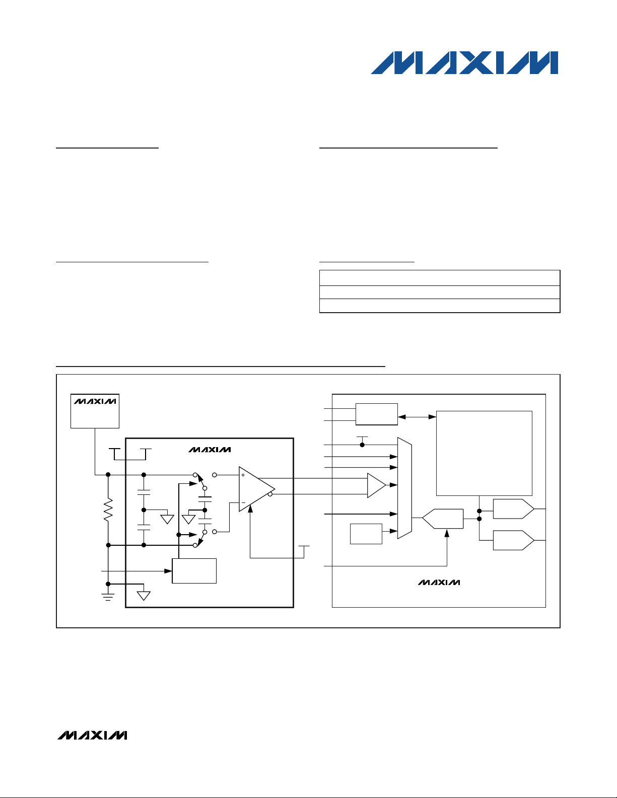
Detailed Description
The DS1843 consists of a fully differential sampling
capacitor, switches, and a differential output buffer. It is
designed to operate in fiber optic burst-mode systems;
however, it can be used in other applications requiring
a fast sample-and-hold circuit. The output can be configured for single-ended operations.
Input Sampling Capacitor
The input voltage is sampled using a 5pF capacitor on
the positive input and another on the negative input.
The capacitors are connected to the input when SEN is
high. In addition to the sampling capacitors, the inputs
also have parasitic capacitance (CIN). These capacitors must fully charge before SEN is switched to low in
order to ensure accurate sampling. An RC time constant is created by the resistance of the voltage source
connected to the DS1843’s input and the capacitances
on this node. See the
Applications Information
section
for details.
Output Buffer
After sampling is complete, the sampling capacitor is
switched to the output buffer. This buffer requires a
small amount of time to settle, t
OUT
. When an ADC is
used to measure the DS1843’s output, a step occurs at
the ADC’s input caused by the ADC’s internal sampling
capacitor. The DS1843’s recovery time, t
REC
, is dependent on the size of the ADC’s sampling capacitor and
the voltage applied across the ADC. To maximize
accuracy, the ADC’s sampling speed (ADC clock frequency) should be reduced until the ADC’s conversion
window (t
ADC:ST
, as shown in the
Timing Diagram
) is
larger than the DS1843’s recovery time. Refer to the
ADC’s documentation for t
ADC:ST
.
Sampling Time and Output Error
As the sampling time (tS) is decreased, the output error
increases. The output error is largely dependent on the
settling time of the sampling capacitor and, to a lesser
degree, the output buffer’s gain error and offset voltage. Settling time can be reduced by driving the
DS1843 with a lower impedance. In a typical fiber optic
application, a current is applied across a 5kΩ resistor.
By using a stronger current source, the resistance and
the settling time can be reduced (see the
Applications
Information
section for details).
Pin Description
Block Diagram
PIN NAME FUNCTION
1 VCC Power-Supply Input
2 V
3 V
4 DEN Different ia l Output Enable. Connect to VCC for differentia l output or GND for single-ended output.
5 GND Ground Termina l
6 V
7 V
8 SEN Sample Enable. Enables input sampl ing. This input is pulsed.
Positive Voltage Input. Input to sample circuit.
INP
Negative Voltage Input. Input to sample circuit.
INN
OUTN
OUTP
Sampled Voltage Negative Output. Buffered output of the hold capacitor. Keep unconnected or
connect to GND for single-ended output mode.
Sampled Voltage Pos itive Output and Single-Ended Output. Buffered output of the hold capacitor.
V
V
V
SEN
GND
CC
INP
INN
C
IN
C
IN
DS1843
CONTROL
LOGIC
V
OUTN
V
C
S
C
S
OUTP
DEN
Page 7

DS1843
Fast Sample-and-Hold Circuit
_______________________________________________________________________________________ 7
Applications Information
Power-Supply Decoupling
To achieve the best results when using the DS1843,
decouple the power-supply pin, VCC, with a 0.01μF or
0.1μF capacitor. Use a high-quality X7R or equivalent
ceramic surface-mount capacitor.
DS1843 Estimated Settling Time
The settling time is dependent on the gain ratio of the
current mirror used at the input of the DS1843. For
example, the MAX4007 includes a 10:1 ratio current
mirror. This requires a 5kΩ resistor to create a 1V fullscale output with 2mA current input to the MAX4007.
This resistor can be decreased to 2.5kΩ by using the
DS1842, which has a 5:1 ratio current mirror.
Variable Definitions:
RIN: Input resistor. The current mirror creates a voltage
across this resistor.
RSW: Resistance of series switch that connects internal
circuitry to input pins after t
IST
time.
CIN: 7pF parasitic (ESD) capacitor.
C
PAR
: External parasitic capacitance. A current mirror's
output and typical trace capacitance are less than
10pF.
C
S
: 5pF sample capacitor.
t
IST
: Internal settling time based on tSfrom the AC electrical specification. The minimum tSincludes one time
constant. t
IST
removes this time constant.
tRC: RC settling time of the input.
Figure 1 shows the simplified diagram of input impedances for settling time calculations. Sample time is
divided into two parts:
1) t
IST
: Internal settling time (max 250ns). During this
time, voltage VIN(V
INP
- V
INN
) rises with a time con-
stant of:
R
IN
x (CIN+ C
PAR
)
2) tRC: During this period two things happen:
a. Input VINkeeps increasing from its value at t
IST
to its final value with a new time constant of:
b. RSWand CStrack this VIN(input) with a time constant of RSWx CS, which is 12.5ns (worst case).
Example:
Approximate accuracy calculations can be done for an
input voltage based on the above impedance values.
These calculations can be divided into three parts.
1) Accuracy of input at t
IST
(250ns):
where t1= t
IST
= 250ns.
At t
IST
the internal circuit tags input impedance.
This causes charge redistribution to occur, which
causes a dip in the input voltage. The worst-case
value of the input voltage at t
IST
is:
Figure 1. Input Impedances for Settling Time Calculations Diagram
CURRENT
MIRROR OUTPUT
V
INP
C
PAR
R
IN
V
INN
DS1843
INPUT MODEL
R
SW
C
IN
C
R
IN
SW
C
S
C
S
⎧
RCC R C
×+
⎨
⎩
()
()
IN IN PAR SW S
2
+×
()
2
⎫
⎬
⎭
Accuracy e
=−
⎡
RCC
IN IN PAR
⎣
1
t
−
1
×+
()
⎤
⎦
V
IN t
@
⎡
=−
11
⎢
IST
⎢
⎣
C
S
CC C
++
()
IN PAR S
⎡
⎤
⎢
⎥⎥×−
⎢
⎢
⎦
⎢
⎣
−
t
IST
⎡
RRCC
×+
()
IN IN PAR
⎣
e
⎤
⎥
⎤
⎦
×
V
⎥
IN
⎥
⎥
⎦
Page 8

2) Accuracy of internal circuitry between tS- t
IST
:
where t2= (tS- t
IST
) and (RSWx CS) ~ = 12ns.
3) Total accuracy of input at sampling time, tS:
μ
×
Pin Configuration
PACKAGE TYPE PACKAGE CODE DOCUMENT NO.
8 μDFN L822+1
21-0164
Package Information
For the latest package outline information and land patterns, go to www.maxim-ic.com/packages.
Maxim cannot assume responsibility for use of any circuitry other than circuitry entirely embodied in a Maxim product. No circuit patent licenses are
implied. Maxim reserves the right to change the circuitry and specifications without notice at any time.
8
_____________________Maxim Integrated Products, 120 San Gabriel Drive, Sunnyvale, CA 94086 408-737-7600
© 2009 Maxim Integrated Products Maxim is a registered trademark of Maxim Integrated Products, Inc.
Fast Sample-and-Hold Circuit
DS1843
Accuracy e
=−
1
t
−
2
RC
×
()
SW S
TOP VIEW
V
CC
Accuracy V e
where newRC R C C R C
⎡
⎢
=−−
11 1
()
IN t
@
⎢
⎣
=×+
IST
⎧
⎨
⎩
()
()
IN IN PAR SW S
×
−
newRC
t
⎤
2
⎥
×
⎥
⎦
2
⎡
⎢
⎢
⎢
⎣
+×
−
t
⎤
2
⎥
×
RC
()
SW S
−−
e
()
⎥
⎥
⎦
2
⎫
⎬⎬
⎭
V
INP
V
INN
DEN GND
+
1
2
DS1843
3
4
DFN
2mm)
(2mm
8
SEN
V
7
OUTP
V
6
OUTN
5
 Loading...