

Page 1
General Description
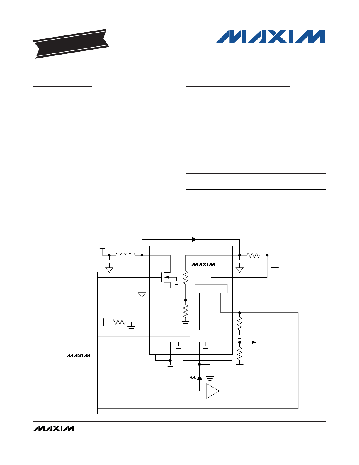
The DS1842A integrates the discrete high-voltage
components necessary for avalanche photodiode
(APD) bias and monitor applications. A switch FET and
precision voltage-divider network are used in conjunction with an external DC-DC controller to create a boost
DC-DC converter. A current clamp limits current
through the APD and also features an external shutdown. The precision voltage-divider network is provided for precise control of the APD bias voltage. The
device also includes a dual current mirror to monitor
the APD current.
Applications
APD Biasing
GPON ONU and OLT
Features
♦ 76V Maximum Boost Voltage
♦ Switch FET
♦ Current Monitor with a Wide 1µA to 2mA Range,
Fast 50ns Time Constant, and 10:1 and 5:1 Ratio
♦ 2mA Current Clamp with External Shutdown
♦ Precision Voltage Feedback
♦ Multiple External Filtering Options
♦ 3mm x 3mm, 14-Pin TDFN Package with Exposed Pad
DS1842A
76V, APD, Bias Output Stage with
Current Monitoring
________________________________________________________________
Maxim Integrated Products
1
Ordering Information
19-4994; Rev 0; 10/09
For pricing, delivery, and ordering information, please contact Maxim Direct at 1-888-629-4642,
or visit Maxim’s website at www.maxim-ic.com.
EVALUATION KIT
AVAILABLE
PART TEMP RANGE PIN-PACKAGE
DS1842AN + -40°C to +85°C 14 TDFN-EP*
DS1842AN +T& R -40°C to +85°C 14 TDFN-EP*
+
Denotes a lead(Pb)-free/RoHS-compliant package.
T&R = Tape and reel.
*
EP = Exposed pad.
DS1875
DS1842A
SW
FB
D2
COMP
MON3
LX
GATE
PGND
FBOUT
R
1
R
2
MIRIN
FBIN
MIR1
CLAMP
NOTE: SEE THE LAYOUT CONSIDERATIONS SECTION.
MIROUTGNDEP
3.3V
CURRENT MIRROR
CURRENT
LIMIT
MIR2
C
BULK
C
COMP
R
COMP
EXTERNAL MONITOR
TIA
APD
ROSA
Typical Application Circuit
Page 2

DS1842A
76V, APD, Bias Output Stage with
Current Monitoring
2 _______________________________________________________________________________________
ABSOLUTE MAXIMUM RATINGS
ELECTRICAL CHARACTERISTICS
(TA= -40°C to +85°C, unless otherwise noted.)
Stresses beyond those listed under “Absolute Maximum Ratings” may cause permanent damage to the device. These are stress ratings only, and functional
operation of the device at these or any other conditions beyond those indicated in the operational sections of the specifications is not implied. Exposure to
absolute maximum rating conditions for extended periods may affect device reliability.
Note 1: Rising MIROUT transition from 10µA to 1mA; V
MIRIN
= 40V, 2.5kΩ load.
Note 2: Not production tested. Guaranteed by design.
Voltage Range on GATE and CLAMP
Relative to GND...................................................-0.3V to +12V
Voltage Range on MIRIN, MIROUT, FBIN
MIR1, and MIR2 Relative to GND........................-0.3V to +80V
Voltage Range on FBOUT Relative to GND ..........-0.3V to +6.0V
Voltage Range on LX Relative to GND...................-0.3V to +85V
Operating Junction Temperature Range...........-40°C to +150°C
Storage Temperature Range .............................-55°C to +135°C
Soldering Temperature ..........................Refer to the IPC JEDEC
J-STD-020 Specification.
Switching Frequenc y f
FET Capacitance
FET Gate Res is tance R
FET On-Res is tance R
GATE Voltage V
Switching Current I
LX Voltage V
LX Leakage I
CLAMP Voltage V
CLAMP Threshold V
Maximum MIROUT Current I
MIR1 to MIROUT Ratio K
MIR2 to MIROUT Ratio K
MIR1, MIR2 Rise Time
(20%/80%)
Shutdown Temperature T
Hysteresis Temperature T
Leakage on GATE and CLAMP IIL -1 +1 μA
Resistor-Divider Ratio (R1/R2) KR TA = +25°C, V
Resistor-Di vider Tempco ±50 ppm/°C
Resistor-Divider End-to-End
Resistance
PARAMETER S YMBOL CONDITIONS MIN TYP MAX UNITS
SW
C
GATE VGS
C
DSON
GS
LX
LX
IL(LX)
CLAMP
CLT
MIROUT
MIR1
MIR2
t
RC
SHDN
HYS
R
RES
0 1.2 MHz
= 0V, V
fSW= 1MHz 90
LX
22
G
V
= 3V, ID= 170mA 1 2
GS
V
= 10V, ID= 170mA 0.75 1.4
GS
0 11 V
Duty cycle = 10%, fSW= 100kHz 680 mA
80 V
V
0 11 V
1.25 1.8 2.35 V
(Note 2) 5 °C
TA = +25°C, V
= 0V, V
GATE
CLAMP = low 1.8 2.75 3.85 mA
CLAMP = high 10 μA
15V < V
MIRIN
15V < V
MIRIN
(Note 1) 30 ns
(Note 2) +150 °C
= 25V 40
DS
= 76V -1 +1 μA
LX
< 76V, I
< 76V, I
= 76V 59.5 60.25
FBIN
= 76V 308 385 481 k
FBIN
> 1μA 0.096 0.100 0.104 A/A
MIROUT
> 1μA 0.192 0.200 0.208 A/A
MIROUT
pF
Page 3
DS1842A
76V, APD, Bias Output Stage with
Current Monitoring
_______________________________________________________________________________________
3
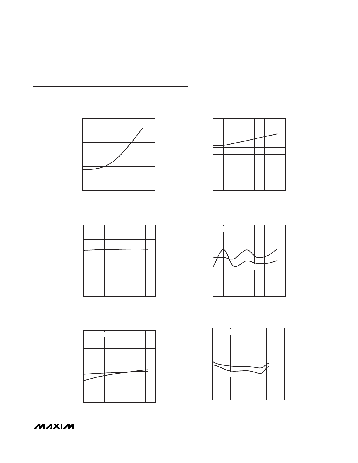
Typical Operating Characteristics
(TA = +25°C, unless otherwise noted.)
MIRIN CURRENT vs. MIROUT CURRENT
(V
10,000
1000
100
MIRIN CURRENT (μA)
10
1 10,000
MIRIN
MIROUT CURRENT (μA)
MIRIN CURRENT vs. TEMPERATURE
= 40V, I
(V
MIRIN
5
4
3
2
MIRIN CURRENT (mA)
1
= 40V)
MIROUT
100010010
= 2mA)
DS1842A toc01
DS1842A toc03
MIRIN CURRENT vs. TEMPERATURE
= 40V, I
(V
100
MIRIN CURRENT (μA)
MIRIN
90
80
70
60
50
40
30
20
10
0
-40 100
TEMPERATURE (°C)
MIR ERROR vs. TEMPERATURE
(I
2
1
0
ERROR (%)
-1
V
MIRIN
MIROUT
= 40V
MIR2
MIROUT
= 1μA)
MIR1
= 250nA)
DS1842A toc02
806020 400-20
DS1842A toc04
0
-40 100
TEMPERATURE (°C)
MIR ERROR vs. TEMPERATURE
= 1mA)
(I
2
V
MIRIN
1
0
ERROR (%)
-1
-2
-40 100
MIROUT
= 40V
MIR2
MIR1
TEMPERATURE (°C)
806040200-20
DS1842A toc05
806040200-20
-2
-40 100
TEMPERATURE (°C)
MIR ERROR vs. MIROUT CURRENT
2
V
= 40V
MIRIN
1
0
ERROR (%)
-1
-2
1 10,000
MIR2
MIR1
MIROUT CURRENT (μA)
806040200-20
DS1842A toc06
100010010
Page 4
DS1842A
76V, APD, Bias Output Stage with
Current Monitoring
4 _______________________________________________________________________________________
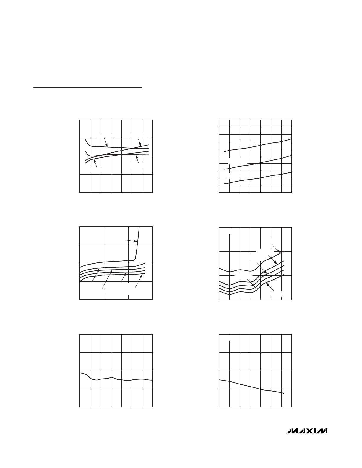
Typical Operating Characteristics (continued)
(TA = +25°C, unless otherwise noted.)
ERROR (%)
-1
-2
2.0
1.5
(Ω)
1.0
DSON
R
0.5
MIR ERROR
vs. MIRIN VOLTAGE
2
I
= 1μA
I
MIR1
MIR2
= 1mA
MIRIN VOLTAGE (V)
1
0
10 80
I
MIR2
I
MIR1
= 1mA
= 1μA
706050403020
FET ON-RESISTANCE
vs. DRAIN CURRENT
VGS = 2.5V
VGS = 3.0V
VGS = 3.6V
0
1 1000
VGS = 5V
VGS = 10V
10010
IDS (mA)
DS1842A toc07
DS1842A toc09
MIROUT CLAMP CURRENT
vs. MIRIN VOLTAGE
3.5
3.4
3.3
3.2
3.1
(mA)
3.0
MIROUT
I
2.9
2.8
2.7
2.6
2.5
10 80
TA = -40°C
TA = +25°C
TA = +85°C
MIRIN VOLTAGE (V)
FET ON-RESISTANCE
vs. TEMPERATURE
2.0
ID = 170mA
VGS = 2.5V
1.5
(Ω)
DSON
R
1.0
0.5
-40 100
VGS = 5.0V
VGS = 3.0V
VGS = 3.6V
VGS = 10V
TEMPERATURE (°C)
DS1842A toc08
706040 503020
DS1842A toc10
806040200-20
RESISTOR-DIVIDER RATIO
vs. FBIN VOLTAGE
60.1
60.0
)
R
59.9
RATIO (K
59.8
59.7
10 80
FBIN VOLTAGE (V)
60.00
DS1842A toc11
706050403020
59.95
)
R
59.90
RATIO (K
59.85
59.80
RESISTOR-DIVIDER RATIO
vs. TEMPERATURE
V
= 40V
FBIN
-40 100
TEMPERATURE (°C)
DS1842A toc12
806040200-20
Page 5
DS1842A
76V, APD, Bias Output Stage with
Current Monitoring
_______________________________________________________________________________________ 5
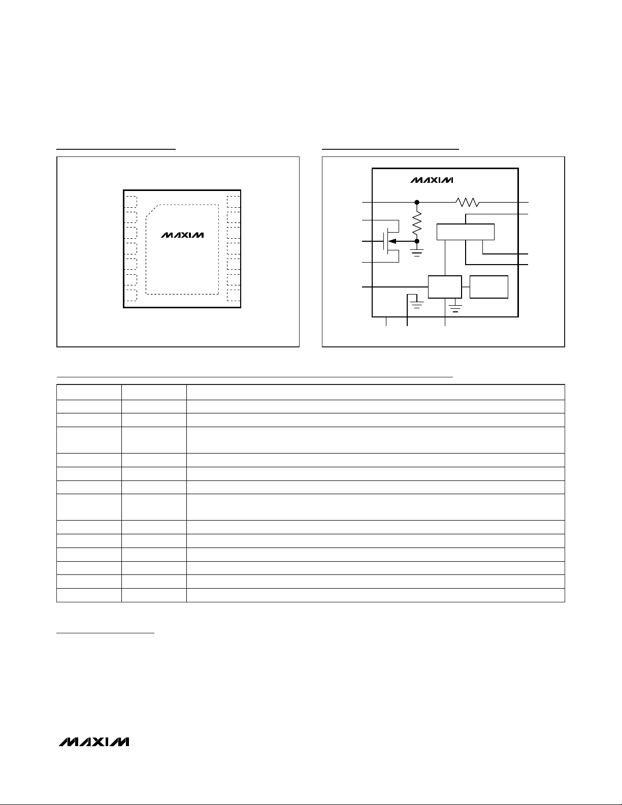
Pin Description
Block Diagram
TDFN
TOP VIEW
2
4
5
13
11
10
MIRIN
N.C.
N.C.
MIR2
FBOUT
CLAMP
1
14
MIROUTMIR1
3
12
FBINGND
6
9
N.C.GATE
7
8
LXPGND
DS1842A
*EP
*EXPOSED PAD.
+
DS1842A
LX
GATE
PGND
MIRIN
MIR1
CLAMP
MIROUT
CURRENT MIRROR
CURRENT
LIMIT
FBIN
MIR2
THERMAL
SHUTDOWN
FBOUT
R
1
R
2
GNDEP
Pin Configuration
Detailed Description
The DS1842A contains discrete high-voltage components required to create an APD bias voltage and to
monitor the APD bias current. The device’s mirror outputs are a current that is a precise ratio of the output
current across a large dynamic range. The mirror
response time is fast enough to comply with GPON Rx
burst-mode monitoring requirements. The device has a
built-in current-limiting feature to protect APDs. The
APD current can also be shut down by CLAMP or thermal shutdown. The internal FET and resistor-divider are
used in conjunction with a DC-DC boost controller to
precisely create the APD bias voltage.
Current Mirror
The DS1842A has two current mirror outputs. One is a
10:1 mirror connected at MIR1, and the other is a 5:1
mirror connected to MIR2.
PIN NAME FUNCTION
1 MIR1 Current Mirror Monitor Output, 10:1 Rat io
2 MIR2 Current Mirror Monitor Output, 5:1 Ratio
3 GND
4 FBOUT Feedback Output. Resistor-divider output.
5 CLAMP Clamp Input. Disables the current mirror output (MIROUT).
6 GATE FET Gate Connection
7 PGND
8 LX FET Drain Connection. Connect to switching inductor.
9, 10, 11 N.C. No Connection
12 FBIN Feedback Input. Res istor-divider input.
13 MIRIN Current Mirror Input
14 MIROUT Current Mirror Output. Connect to APD bia s pin.
— EP Exposed Pad. Connect direct ly to the same ground plane as GND.
Ground Connection for Device. Connect d irectly to ground plane. Connect GND to PGND at a
single point. See the Layout Considerations section for more information.
Source of Switch FET. A lso connect to boost converter’s input and output capacitors. Connect
PGND to GND at a single point. See the Layout Considerations section for more information.
Page 6
The mirror output is typically connected to an ADC
using a resistor to convert the mirrored current into a
voltage. The resistor to ground should be selected such
that the maximum full-scale voltage of the ADC is
reached when the maximum mirrored current is
reached. For example, if the maximum monitored current through the APD is 2mA with a 1V ADC full scale,
and the 10:1 mirror is used, then the correct resistor is
approximately 5kΩ. If both MIR1 and MIR2 are connected together, the correct resistor is 1.6kΩ.
The mirror response time is dominated by the amount of
capacitance placed on the output. For burst-mode Rx
systems where the fastest response times are required
(approximately a 50ns time constant), a 3.3pF capacitor
and external op amp should be used to buffer the signal
sent to the ADC. For continuous mode applications, a
10nF capacitor is all that is required on the output.
Current Clamp
The DS1842A has a current clamping circuit to protect
the APD by limiting the amount of current from MIROUT.
There are three methods of current clamping available:
1) Internally Defined Current Limit
The device’s current clamp circuit automatically
clamps the current when it exceeds the maximum
MIROUT current.
2) External Shutdown Signal
The CLAMP pin can completely shut down the current
from MIROUT. The CLAMP pin is active high.
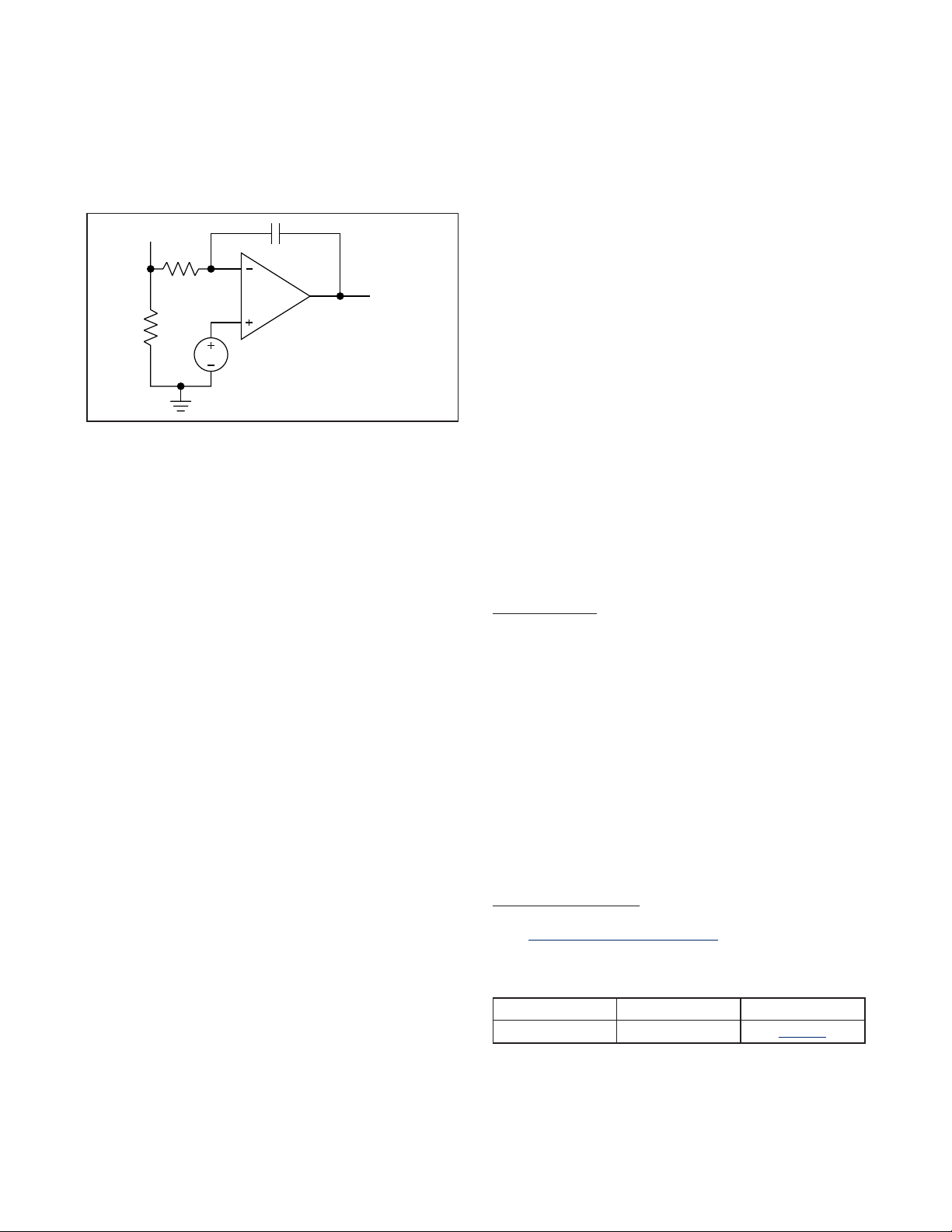
3) Precise Level Set by External Feedback Circuit
A feedback circuit is used to control the level applied to
the CLAMP pin. Figure 1 shows an example feedback
circuit.
Thermal Shutdown
As a safety feature, the DS1842A has a thermal-shutdown circuit that turns off the MIROUT and MIRIN currents when the internal die temperature exceeds
T
SHDN
. These currents resume after the device has
cooled.
Switch FET
The DS1842A switching FET is designed to complement the DS1875 controller’s built-in DC-DC boost controller. APD biasing of 16V to 76V can be achieved
using the DS1842A.
Precision Voltage-Divider
The DS1842A includes a resistor-divider to use as the
feedback network for the boost converter. The
DS1842A resistor-divider ratio, K
R(R1/R2
), is tightly
controlled, allowing the boost converter output to be set
with very high precision. KRcan pair with the DS1875’s
internal DC-DC boost controller. KRcan also be easily
modified by adding external series/parallel resistors;
however, the temperature coefficient of the external
resistors must be considered.
Applications Information
Layout Considerations
Proper PCB layout helps reduce switching noise in the
system. PGND is the connection of the switching FET
and thus carries high current pulses. PGND should also
be connected to the boost converter’s input capacitor
and output bulk capacitor. Ensure that the PGND trace
is low impedance and able to carry the high current
from the FET. To keep the switching noise on PGND
isolated from GND, a star ground configuration should
be used. PGND and GND should only be connected
together at one point on the PCB. This point can be
either the ground side of the output bulk capacitor or
the common ground point of the PCB. Keeping all PCB
traces as short as possible reduces radiated noise,
stray capacitance, and trace resistance.
Package Information
For the latest package outline information and land patterns,
go to www.maxim-ic.com/packages
. Note that a “+”, “#”, or
“-” in the package code indicates RoHS status only. Package
drawings may show a different suffix character, but the drawing
pertains to the package regardless of RoHS status.
DS1842A
76V, APD, Bias Output Stage with
Current Monitoring
Maxim cannot assume responsibility for use of any circuitry other than circuitry entirely embodied in a Maxim product. No circuit patent licenses are
implied. Maxim reserves the right to change the circuitry and specifications without notice at any time.
6
_____________________Maxim Integrated Products, 120 San Gabriel Drive, Sunnyvale, CA 94086 408-737-7600
© 2009 Maxim Integrated Products Maxim is a registered trademark of Maxim Integrated Products, Inc.
CLAMP
MIR1
REF
Figure 1. Current Clamp from Current Feedback
PACKAGE TYPE PACKAGE CODE DOCUMENT NO.
14 TDFN-EP T1433+2
21-0137
 Loading...