

Page 1
ma
r
(
)
(
)
2
4
8
5
G
PRELIMINARY
DS1821
Programmable Digital Thermostat and
Thermomete
FEATURES
Requires no external components
Unique 1-Wire
port pin for communication
Operates over a -55°C to +125°C (67°F to
+257°F) temperature range
Functions as a standalone thermostat with
user-definable trip-points
Provides 8-bit (1°C resolution) centigrade
temperature measurements
Accuracy is ±1°C over 0°C to +85°C range
Converts temperature to a digital word in 1
second (max)
Available in 3-pin PR35 and 8-pin SOIC
packages
Applications include thermostatic controls,
industrial systems, consumer products,
thermometers, or any thermally sensitive
system
®
interface requires only one
PIN ASSIGNMENT
DALLAS
DS1821
1
23
DD
DQ
V
GND
1
23
BOTTOM VIEW
DQ
ND
NC
NC
1
DS1821S
3
8-pin 208-mil SOIC
DS1821S
V
DD
7
NC
6
NC
NC
PR35
(DS1821)
PIN DESCRIPTION
GND - Ground
DQ - Data In/Out and Thermostat Output
V
DD
- Power Supply Voltage
NC - No Connect
DESCRIPTION
The DS1821 can function as a standalone thermostat with user-programmable trip-points or as 8-bit
temperature sensor with a 1-wire digital interface. The thermostat trip-points are stored in nonvolatile
memory, so DS1821 units can be programmed prior to system insertion for true standalone operation.
The DS1821 has an operating temperature range of –55°C to +125°C and is accurate to ±1°C over a range
of 0°C to +85°C. Communication with the DS1821 is accomplished through the open-drain DQ pin; this
pin also serves as the thermostat output.
1 of 17 040601
Page 2
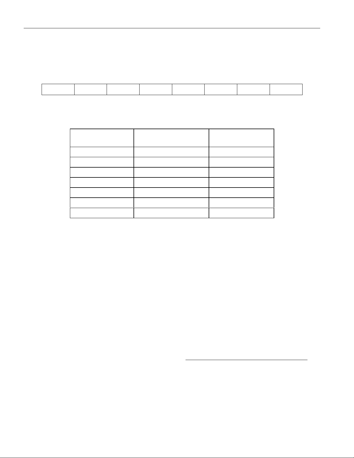
DETAILED PIN DESCRIPTIONS Table 1
GIS
A
V
PR35 8-PIN
SOIC*
SYMBOL DESCRIPTION
DS1821
1 2 GND
Ground pin.
21 DQOpen drain data input/output pin – 1-wire operation; Open drain
thermostat output pin –thermostat operation.
38 V
DD
Power supply pin.
*All pins not specified in this table are “No Connect” pins.
OVERVIEW
Figure 1 shows a block diagram of the DS1821 and pin descriptions are given in Table 1. The DS1821
can operate as a standalone thermostat with user-programmable trip-points or as 8-bit temperature sensor
with a 1-wire digital interface. The open-drain DQ pin functions as the thermostat output for thermostat
operation and as the data I/O pin for 1-wire communications. The 1-wire interface provides user access to
the nonvolatile (EEPROM) thermostat trip-point registers (TH and TL), the status/configuration register,
and the temperature register.
When configured as standalone thermostat, temperature conversions start immediately at power-up. In
this mode, the DQ pin becomes active when the temperature of the DS1821 exceeds the limit
programmed into the TH register, and remains active until the temperature drops below the limit
programmed into the TL register.
The DS1821 uses Dallas’ exclusive 1-wire bus protocol that implements bus communication with one
control signal. This system is explained in detail in the 1-WIRE BUS SYSTEM section of this datasheet.
DS1821 BLOCK DIAGRAM Figure 1
CONFIGURATION REGISTER
ND CONTROL LOGIC
TEMPERATURE SENSOR
TH REGISTER
TL RE
TER
DIGITAL
COMPARATOR/
LOGIC
4.7K
V
DD
DQ
DD
GND
DS1821
1-WIRE
INTERFACE
AND
I/O CONTROL
POWER
SUPPLY
SENSE
TEMPERATURE SENSOR FUNCTIONALITY
The core functionality of the DS1821 is its proprietary direct-to-digital temperature sensor, which
provides 8-bit (1°C increment) centigrade temperature readings over the range of -55°C to +125°C.
A block diagram of the temperature measurement circuitry is shown in Figure 2. This circuit measures
the temperature by counting the number of clock cycles generated by an oscillator with a low temperature
coefficient (temp-co) during a gate period determined by a high temp-co oscillator. The low temp-co
Page 2 of 17
Page 3
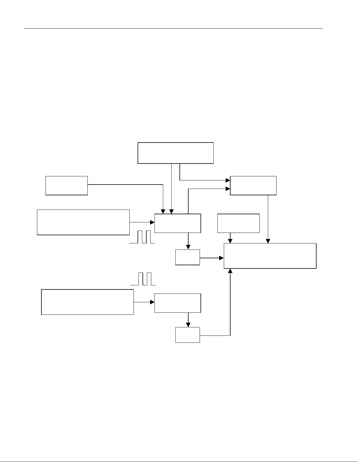
DS1821
counter is preset with a base count that corresponds to –55°C. If the counter reaches 0 before the gate
period is over, the temperature register, which is preset to –55°C, is incremented by one degree, and the
counter is again preset with a starting value determined by the slope accumulator circuitry. The preset
counter value is unique for every temperature increment and compensates for the parabolic behavior of
the oscillators over temperature.
At this time, the counter is clocked again until it reaches 0. If the gate period is not over when the counter
reaches 0, the temperature register is incremented again. This process of presetting the counter, counting
down to zero, and incrementing the temperature register is repeated until the counter takes less time to
reach zero than the duration of the gate period of the high temp-co oscillator. When this iterative process
is complete, the value in the temperature register will indicate the centigrade temperature of the device.
TEMPERATURE MEASURING CIRCUITRY Figure 2
SLOPE ACCUMULATOR
PRESET COMPARE
LOW TEMPERATURE
COEFFICIENT OSCILLATOR
HIGH TEMPERATURE
COEFFICIENT OSCILLATOR
COUNTER PRESET
INC
=0
COUNTER
STOP
=0
TEMPERATURE REGISTER
SET/CLEAR
LSB
OPERATING MODES
The DS1821 has two operating modes: 1-wire mode and thermostat mode. The power-up operating mode
is determined by the user-programmable T/R¯ bit in the status/configuration register: if T/R¯ = 0 the device
powers-up in 1-wire mode, and if T/R¯ = 1 the device powers-up in thermostat mode. The T/R¯ bit is
stored in nonvolatile memory (EEPROM), so it will retain its value when the device is powered down.
1-WIRE MODE
The DS1821 arrives from the factory in 1-wire mode (T/R¯ = 0). In this mode, the DQ pin of the DS1821
is configured as a 1-wire port for communication with a microprocessor using the protocols described in
Page 3 of 17
Page 4

DS1821
the 1-WIRE BUS SYSTEM section of this datasheet. These communications can include reading and
writing the high and low thermostat trip-point registers (TH and TL) and the configuration register, and
reading the temperature, counter, and slope accumulator registers. Also in this mode, the microprocessor
can initiate and stop temperature measurements as described in the OPERATION – MEASURING
TEMPERATURE section of this datasheet.
The T
and T
H
registers and certain bits (THF, TLF, T/R¯, POL and 1SHOT) in the status/configuration
L
register are stored in nonvolatile EEPROM memory, so they will retain data when the device is powered
down. This allows these registers to be pre-programmed when the DS1821 is to be used as a standalone
thermostat. Writes to these nonvolatile registers can take up to 10ms. To avoid data corruption, no
writes to nonvolatile memory should be initiated while a write to nonvolatile memory is in progress.
Nonvolatile write status can be monitored by reading the NVB bit in the status/configuration register:
NVB = 0 – a write to EEPROM memory is in progress, NVB = 0 – nonvolatile memory is idle.
THERMOSTAT MODE
In thermostat mode (T/R¯ = 1), the DS1821 can operate as a standalone thermostat that triggers according
to the TH and TL trip-points programmed while the device was in 1-wire mode. In thermostat mode the
DS1821 powers-up performing continuous temperature conversions, and the DQ pin acts as the
thermostat output. Detailed operation of the thermostat output is provided in the OPERATION –
STANDALONE THERMOSTAT section of this datasheet.
Communications can be re-establish with the DS1821 while it is in thermostat mode by pulling VDD to 0V
while the DQ line is held high, and then toggling the DQ line low 16 times as shown in Figure 12. This
temporarily places the DS1821 in 1-wire mode, allowing microprocessor communication with the
DS1821 via the DQ pin. At this time any I/O function can be performed, such as reading/writing the TH,
TL or configuration registers or reading the temperature register. To return to thermostat mode, the same
procedure can be performed (pulling VDD to 0V while the DQ line is held high, and then clocking the DQ
line 16 times) or the power can be cycled. Note that temporarily putting the DS1821 into 1-wire mode
does not change the power-up mode of the device; this can only be changed by rewriting the T/R¯ bit in
the status/configuration register. Also note that holding both V
approximately 10 seconds will cause the DS1821 to be powered down.
and DQ low for more than
DD
OPERATION – MEASURING TEMPERATURE
DS1821 output temperature data is calibrated in degrees centigrade and is stored in two’s complement
format in the 1-byte (8-bit) temperature register (see Figure 3), which the user can access when the
DS1821 is in 1-wire mode (T/R¯ = 0 in the status/configuration register). The sign bit (S) indicates if the
temperature is positive or negative; for positive numbers S = 0 and for negative numbers S = 1. Table 2
gives examples of digital output data and the corresponding temperature reading. For Fahrenheit
measurements, a lookup table or conversion routine must be used.
The DS1821 can be configured by the user to take continuous temperature measurements (continuous
conversion mode) or single measurements (one-shot mode). The desired configuration can be achieved
by setting the nonvolatile1SHOT bit in the status/configuration register: 1SHOT = 0 – continuous
conversion mode, 1SHOT = 1 – one-shot mode. Note that the 1SHOT setting only controls the operation
of the device in 1-wire mode; in thermostat mode, continuous temperature conversions are started
automatically at power-up.
In continuous conversion mode, the Start Convert T [EEh] command initiates continuous temperature
conversions, which can be stopped using the Stop Convert T [22h] command. In one-shot mode the Start
Convert T [EEh] command initiates a single temperature conversion after which the DS1821 returns to a
low-power standby state. In this mode, the microprocessor can monitor the DONE bit in the
Page 4 of 17
Page 5
DS1821
configuration register to determine when the conversion status: DONE = 0 ― conversion in progress,
DONE = 1 ― conversion complete. The DONE bit does not provide conversion status in continuous
conversion mode since measurements are constantly in progress (i.e., DONE will always be 0).
TEMPERATURE, TH and TL REGISTER FORMAT Figure 3
bit 7 bit 6 bit 5 bit 4 bit 3 bit 2 bit 1 bit 0
S262
5
4
2
3
2
2
2
1
2
0
2
TEMPERATURE/DATA RELATIONSHIP Table 2
TEMPERATURE DIGITAL OUTPUT
(Binary)
DIGITAL OUTPUT
(Hex)
+125°C* 0111 1101 7Dh
+85°C 0101 0101 55h
+25°C 0001 1001 19h
0°C 0000 0000 00h
-1°C 1111 1111 FFh
-25°C 1110 0111 E7h
-55°C 1100 1001 C9h
HIGH-RESOLUTION TEMPERATURE READINGS
The user can calculate temperature values with higher than 8-bit resolution using the data remaining in
the counter and slope accumulator when the temperature conversion is complete. To do this the user must
first read the temperature from the 8-bit temperature register. This value is called TEMP_READ in the
high-resolution equation (see Eq. 1). The 9-bit counter value must then be obtained by issuing the Read
Counter [A0h] command. This value is the count remaining in the counter at the end of the gate period
and is called COUNT_REMAIN in Eq. 1. Next the Load Counter [41h] command must be issued, which
loads the 9-bit slope accumulator value into the counter register. The slope accumulator value (called
COUNT_PER_C in Eq. 1) can then be read from the counter by again issuing the Read Counter [A0h]
command. The slope accumulator value is called “COUNT_PER_C” because it represents the number of
counts needed for an accurate measurement at a given temperature (i.e., the counts per degree C). The
high-resolution temperature can then be calculated using Eq. 1:
Eq. 1) TEMPERATURE = TEMP_READ − 0.5 +
REMAINCOUNTCPERCOUNT
CPERCOUNT
__
)___( −
Additional information about high-resolution temperature calculations can be found in Application Note
105: “High Resolution Temperature Measurement with Dallas Direct-to-Digital Temperature Sensors”.
Page 5 of 17
Page 6
DS1821
(DQ
)
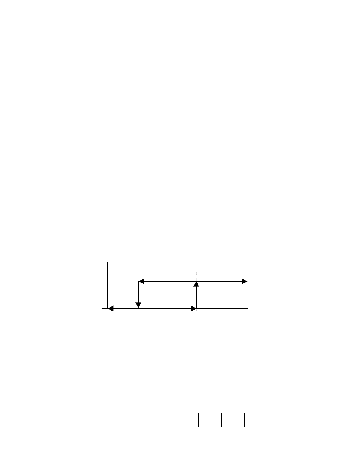
OPERATION – THERMOSTAT
When the DS1821 is in thermostat mode (T/R¯ = 1 in the status/configuration register), temperature
conversions are performed continuously beginning at power-up (regardless of the value of the 1SHOT
bit), and the DQ pin serves as the thermostat output. The DQ output will become active when the
temperature of the DS1821 exceeds the user-defined limit in the TH register, and will remain active until
the temperature drops below the user-defined limit in the TL register as illustrated in Figure 4. Thus, the
user can select TH and TL to provide the desired amount of thermostat output hysteresis.
The user-defined 8-bit centigrade trip-point values (TH and TL) must be stored in two’s complement
format as shown in Figure 3. The sign bit (S) indicates if the temperature is positive or negative; for
positive numbers S = 0 and for negative numbers S = 1. The non-volatile T
programmed when the DS1821 is in 1-wire mode as explained in the OPERATING MODES section of
this datasheet. The DS1821 can be temporarily switched from thermostat mode to 1-wire mode to change
the T
and TL values as also explained in the OPERATING MODES section.
H
The polarity (i.e., the active state) of the DQ output is user-selectable with the nonvolatile POL bit in the
status/configuration register. DQ is active-high when POL = 1, and DQ is active-low when POL = 0.
Two bits in the status/configuration register, THF and TLF, provide additional thermostatic information.
The value of these bits is normally 0. The THF (temperature high flag) bit will be set to 1 if the measured
temperature is ever greater than the value in the TH register and will remain a 1 until the user rewrites the
bit with a 0. The THL (temperature low flag) bit will be set to 1 if the temperature is ever lower than the
value in the TL register and will remain a 1 until the user rewrites the bit with a 0. These bits provide a
record of the device temperature relative to the thermostat trip-points over a period of time. They are
stored in nonvolatile memory, so the data stored in THF and TLF can be analyzed after any number of
power cycles. The THF and THL bits function in both 1-wire and thermostat mode.
and TL registers must be
H
DQ OPERATION IN THERMOSTATE MODE Figure 4
Operating Mode = Thermostat
DQ
POL=1
T
L
is active high
T
H
Temp (°C)
STATUS/CONFIGURATION REGISTER
The status/configuration register provides information to the user about conversion status, EEPROM
activity and thermostat activity. It also allows the user to program various DS1821 options such as
power-up operating mode, thermostat output polarity and conversion mode. The status/configuration
register is arranged as shown in Figure 5 and detailed descriptions of each bit are provided in Table 3.
Note that the THF, THL T/R¯, POL and 1SHOT bits are stored in nonvolatile memory (EEPROM).
CONFIGURATION REGISTER Figure 5
bit 7 bit 6 bit 5 bit 4 bit 3 bit 2 bit 1 bit 0
DONE 1 NVB THF* THL*
*Stored in EEPROM
Page 6 of 17
T/R¯*
POL* 1SHOT*
Page 7

CONFIGURATION REGISTER BIT DESCRIPTIONS Table 3
L
Bit Name
(User Access)
DONE — Temperature Conversion Done
(Read Only)
NVB — Non-volatile Memory Busy
(Read Only)
THF* — Temperature High Flag
(Read/Write)
TLF* — Temperature Low Flag
(Read/Write)
T/R¯* — Power-up Operating Mode
(Read/Write)
POL* — Thermostat Output (DQ) Polarity
(Read/Write)
1SHOT* — Conversion Mode
(Read/Write)
*Stored in EEPROM
DONE = 0 — Temperature conversion is in progress.
DONE = 1 — Temperature conversion is complete.
NVB = 0 — Nonvolatile memory is not busy.
NVB = 1 — A write to EEPROM memory is in progress
THF = 0 — The measured temperature has not exceeded the
value stored in the T
THF = 1 — At some point in time the measured temperature has
been higher than the value stored in the T
remain a 1 until it is over-written with a 0 by the user.
TLF = 0 — The measured temperature has not been lower than
the value stored in the T
TLF = 1 — At some point in time the measured temperature has
been lower than the value stored in the T
remain a 1 until it is over-written with a 0 by the user.
T/R¯ = 0 — DS1821 powers up in 1- wire mode.
T/R¯ = 1 — DS1821 powers up in thermostat mode.
POL = 0 — Thermostat output (DQ) is active low.
POL = 1 — Thermostat output (DQ) is active high.
1SHOT = 0 — Continuous conversion mode. The Start Convert
T [EEh] command initiates continuous temperature conversions,
which can be stopped with the Stop Convert T [22h] command.
1SHOT = 1 — One-shot mode. The Start Convert T [EEh]
command initiates a single temperature conversion after which
the DS1821 returns to a low-power standby state.
Functional Description
register.
H
register.
L
DS1821
register. THF will
H
register. TLF will
Page 7 of 17
Page 8

DS1821
A
1-WIRE BUS SYSTEM
The 1-wire bus system uses a single bus master (i.e., a microprocessor) to control slave devices. The
DS1821 functions as a slave device when it is used in 1-wire mode; however, since the DS1821 is not
addressable or multi-droppable, a single 1-wire-mode DS1821 must be the only slave device on the bus.
All data and commands are transmitted least significant bit first over the 1-wire bus.
The following discussion of the 1-wire bus system is broken down into three topics: hardware
configuration, transaction sequence, and 1-wire signaling (signal types and timing).
HARDWARE CONFIGURATION
The 1-wire bus has by definition only a single data line. Each device (in this case, the master and one
DS1821) interfaces to the data line via an open drain or 3–state port. This allows each device to “release”
the data line when the device is not transmitting data so that the bus is available for use by the other
device. The 1-wire port of the DS1821 (the DQ pin) is open drain with an internal circuit equivalent to
that shown in Figure 6.
The 1-wire bus requires an external pullup resistor of approximately 5 kΩ; thus, the idle state for the 1-
wire bus is high. If for any reason a transaction needs to be suspended, the bus MUST be left in the idle
state if the transaction is to resume. Infinite recovery time can occur between bits so long as the 1-wire
bus is in the inactive (high) state during the recovery period. If the bus is held low for more than 480 µs,
the DS1821 will be reset.
HARDWARE CONFIGURATION Figure 6
Micro-
processor
R
X
T
X
V
DD
4.7K
RX= RECEIVE
= TRANSMIT
T
X
DS1821 1-WIRE PORT
DQ
Pin
1-wire bus
5 µ
Typ.
TRANSACTION SEQUENCE
The transaction sequence for accessing the DS1821 via the 1-wire port is as follows:
R
T
X
100 ΩΩΩΩ
MOSFET
X
• Initialization
• DS1821 Function Command
• Data Transmitted/Received
Page 8 of 17
Page 9

DS1821
INITIALIZATION
All transactions on the 1-wire bus begin with an initialization sequence. The initialization sequence
consists of a reset pulse transmitted by the bus master followed by a presence pulse transmitted by the
DS1821. The presence pulse lets the bus master know that the DS1821 is on the bus and ready to
operate. Timing for the reset and presence pulses is detailed in the 1-WIRE SIGNALING section.
DS1821 FUNCTION COMMANDS
The DS1821 function commands in this section allow the master to communicate with and configure the
DS1821. The DS1821 function commands are summarized in Table 4.
READ TEMPERATURE [AAh]
Provides read access to the 1-byte temperature register.
START CONVERT T [EEh]
Initiates temperature conversions. If the part is in one-shot mode (1SHOT = 1), only one conversion will
be performed. If it is in continuous mode (1SHOT = 0), continuous conversions will be performed until a
Stop Convert T command is received.
STOP CONVERT T [22h]
Stops temperature conversions when the device is in continuous conversion mode (1SHOT = 0). This
opcode has no function if the device is in one-shot mode (1SHOT = 1).
WRITE TH [01h]
WRITE TL [02h]
Provides write access to the 8-bit TH and TL registers, respectively.
READ TH [A1h]
READ TL [A2h]
Provides read access to the 8-bit TH and TL registers, respectively.
WRITE STATUS [0Ch]
Provides write access to the 8-bit status/configuration register.
READ STATUS [ACh]
Provides read access to the 8-bit status/configuration register.
READ COUNTER [A0h]
Provides read access to data in the 9-bit counter register for use in high-resolution temperature
calculations. This is explained in detail in the HIGH-RESOLUTION TEMPERATURE READINGS
section.
LOAD COUNTER [41h]
Loads the 9-bit data from the slope accumulator register into the counter register so that it can be accessed
using the Read Counter [A0h] command. Use of the Load Counter command is explained in detail in the
HIGH-RESOLUTION TEMPERATURE READINGS section.
Page 9 of 17
Page 10

DS1821
DS1821 FUNCTION COMMAND SET Table 4
1-Wire Bus Activity
Command Description Protocol
TEMPERATURE CONVERSION COMMANDS
Read
Temperature
Reads last converted temperature
value from temperature register.
AAh Master receives 8-bit temperature
Start Convert T Initiates temperature conversions. EEh None
Stop Convert T Halts temperature conversions. 22h None
THERMOSTAT and STATUS/CONFIGURATION COMMANDS
Write TH Writes data to the TH register. 01h Master transmits 8-bit TH value to
Write TL Writes data to the TL register. 02h Master transmits 8-bit TL value to
Read TH Reads data from the TH register. A1h Master receives 8-bit TH value from
Read TL Reads data from the TL register. A2h Master receives 8-bit TL value from
After Command is Issued
value from DS1821.
DS1821.
DS1821.
DS1821.
DS1821.
Write Status Writes data to the
status/configuration register.
Read Status
Reads data from the
status/configuration register.
0Ch Master transmits 8-bit
status/configuration value to DS1821.
ACh
Master receives 8-bit
status/configuration value from
DS1821.
HIGH-RESOLUTION COMMANDS
Read Counter
Reads data from the counter
register
Load Counter Loads slope accumulator data into
A0h
Master receives 9-bit counter value
from DS1821.
41h None
the counter register
1-WIRE SIGNALING
The DS1821 uses a strict 1-wire communication protocol to insure data integrity. Several signal types are
defined by this protocol: reset pulse, presence pulse, write 0, write 1, read 0, and read 1. All of these
signals, with the exception of the presence pulse, are initiated by the bus master.
INITIALIZATION PROCEDURE: RESET AND PRESENCE PULSES
All communication with the DS1821 begins with an initialization sequence that consists of a reset pulse
from the master followed by a presence pulse from the DS1821. This is illustrated in Figure 7. When the
DS1821 sends the presence pulse in response to the reset, it is indicating to the master that it is on the bus
and ready to operate given an appropriate function command.
During the initialization sequence the bus master transmits (T
low for a minimum of 480 µs. The bus master then releases the bus and goes into receive mode (R
) the reset pulse by pulling the 1-wire bus
X
X
When the bus is released, the 5k pullup resistor pulls the 1-wire bus high. When the DS1821 detects this
rising edge, it waits 15–60 µs and then transmits a presence pulse by pulling the 1-wire bus low for 60–
240 µs.
Page 10 of 17
).
Page 11

INITIALIZATION TIMING Figure 7
p
p
µ
µµ
µ
µµ
R
DS1821
V
DD
1-WIRE BUS
GND
MASTER TX RESET PULSE MASTER
480
480
µs minimum
DS1821
waits 15-60 µµµµs
LINE TYPE LEGEND
Bus master pulling low
DS1821 pulling low
Resistor
presence pulse
ull-u
µs minimum
DS1821 T
60-240 µµµµs
X
X
READ/WRITE TIME SLOTS
The bus master writes data to the DS1821 during write time slots and reads data from the DS1821 during
read time slots. One bit is data is transmitted over the 1-wire bus per time slot.
WRITE TIME SLOTS
There are two types of write time slots: “Write 1” time slots and “Write 0” time slots. The bus master
uses a Write 1 time slot to write a logic 1 to the DS1821 and a Write 0 time slot to write a logic 0 to the
DS1821. All write time slots must be a minimum of 60 µs in duration with a minimum of a 1 µs recovery
time between individual write slots. Both types of write time slots are initiated by the master pulling the
1-wire bus low (see Figure 8).
To generate a Write 1 time slot, after pulling the 1-wire bus low, the bus master must release the 1-wire
bus within 15 µs. When the bus is released, the 5k pullup resistor will pull the bus high. To generate a
Write 0 time slot, after pulling the 1-wire bus low, the bus master must continue to hold the bus low for
the duration of the time slot (at least 60 µs).
The DS1821 samples the 1-wire bus during a window that lasts from 15 µs to 60 µs after the master
initiates the write time slot. If the bus is high during the sampling window, a 1 is written to the DS1821.
If the line is low, a 0 is written to the DS1821.
READ TIME SLOTS
The DS1821 can only transmit data to the master when the master issues read time slots. Therefore, the
master must generate read time slots immediately after issuing a read command (e.g., Read Temperature
[AAh]), so that the DS1821 can provide the requested data. All read time slots must be a minimum of 60
µs in duration with a minimum of a 1 µs recovery time between slots. A read time slot is initiated by the
master device pulling the 1-wire bus low for a minimum of 1 µs and then releasing the bus (see Figure 8).
After the master initiates the read time slot, the DS1821 will begin transmitting a 1 or 0 on bus. The
DS1821 transmits a 1 by leaving the bus high and transmits a 0 by pulling the bus low. When
transmitting a 0, the DS1821 will release the bus by the end of the time slot, and the bus will be pulled
back to its high idle state by the pullup resister. Output data from the DS1821 is valid for 15 µs after the
falling edge that initiated the read time slot. Therefore, the master must release the bus and then sample
the bus state within 15 µs from the start of the slot.
Page 11 of 17
Page 12

DS1821
µ
µµ
V
µ
µµ
µ
µµ
V
µ
µµ
µ
µµ
µ
µµ
X
µ
µµ
µ
µµ
µ
µµ
X
µ
µµ
µ
µµ
µ
µµ
µ
µµ
µ
µµ
µ
µµ
µ
µµ
Figure 9 illustrates that the sum of T
Figure 10 shows that system timing margin is maximized by keeping T
, TRC, and T
INIT
SAMPLE
must be less than 15 µs for a read time slot.
and TRC as short as possible
INIT
and by locating the master sample time during read time slots towards the end of the 15 µs period.
READ/WRITE TIME SLOT TIMING DIAGRAM Figure 8
LINE TYPE LEGEND (Figure 8, Figure 9 and Figure 10)
Bus master pulling low DS1821 pulling low
Resistor pullup
START
OF SLOT
1 µµµµs < T
15
µs
< ∞
REC
> 1
µs
DS1821 samples
MIN TYP MA
15
µs
30
µs
V
DD
1-WIRE BUS
GND
START
OF SLOT
MASTER WRITE “0 ” SLO T MASTER WRITE “1 ” SLO T
60
µs < TX “0” < 120
DS1821 samples
MIN TYP MA
15
µs
15
µs
30
µs
MASTER READ “0” SLOT MASTER READ “1” SLOT
V
DD
1 µµµµs < T
1-WIRE BUS
GND
> 1
µs
15
µs
> 1
µs
15
µs
Master samples
45
µs
DETAILED MASTER READ 1 TIMING Figure 9
V
DD
1-WIRE BUS
GND
15
T
RC
µs
T
> 1
µs
INT
RECOMMENDED MASTER READ 1 TIMING Figure 10
V
DD
1-WIRE BUS
IH of Master
< ∞
REC
Master samples
IH of Master
Master samples
GND
T
INT
small
=
T
RC
small
=
15
µs
Master samples
Page 12 of 17
Page 13

DS1821
RELATED APPLICATION NOTES
The following Application Notes pertain to the DS1821. These notes can be obtained from the Dallas
Semiconductor “Application Note Book,” via the Dallas website at http://www.dalsemi.com or through
our faxback service at (214) 450–0441.
Application Note 67: “Applying and Using the DS1620 in Temperature Control Applications”
Application Note 74: “Reading and Writing Touch Memories via Serial Interfaces”
Application Note 105: “High Resolution Temperature Measurement with Dallas Direct-to-Digital
Temperature Sensors”
Sample 1-wire subroutines that can be used in conjunction with AN74 can be downloaded from the
Dallas website or anonymous FTP Site.
DS1821 OPERATION EXAMPLE
In this example, the master device programs the DS1821 with T
that the data has been saved correctly. The master then programs the status/configuration register so that
the device will power-up in thermostat mode (T/R¯ = 1) and the thermostat output will have active high
polarity (POL = 1).
= +10°C and TH = +40°C and verifies
L
MASTER
MODE
DATA (LSB
FIRST)
COMMENTS
TX Reset Master issues reset pulse.
RX Presence DS1821 responds with presence pulse.
TX 01h Master issues Write TH command.
TX 28h Master sends data for TH = +40°C.
TX Reset Master issues reset pulse.
RX Presence DS1821 responds with presence pulse.
TX 02h Master issues Write TL command.
TX 0Ah Master sends data for TL = +10°C.
TX Reset Master issues reset pulse.
RX Presence DS1821 responds with presence pulse.
TX A1h Master issues Read TH command.
RX 28h Master reads stored TH value to verify data.
TX Reset Master issues reset pulse.
RX Presence DS1821 responds with presence pulse.
TX A2h Master issues Read TL command.
RX 0Ah Master reads stored TL value to verify data.
TX Reset Master issues reset pulse.
RX Presence DS1821 responds with presence pulse.
TX 0Ch Master issues Write Status command.
TX 06h Master sends status/configuration data to the DS1821 with T/R¯ =
1 (thermostat mode at power-up) and POL = 1 (active high
thermostat output).
Power is cycled; DS1821 powers-up in thermostat mode.
Page 13 of 17
Page 14

DS1821
ABSOLUTE MAXIMUM RATINGS*
Voltage on any pin relative to ground –0.5V to +7.0V
Operating temperature –55°C to +125°C
Storage temperature –55°C to +125°C
Soldering temperature See-JTD-020A Specification
*These are stress ratings only and functional operation of the device at these or any other conditions
above those indicated in the operation sections of this specification is not implied. Exposure to absolute
maximum rating conditions for extended periods of time may affect reliability.
DC ELECTRICAL CHARACTERISTICS (-55°C to +125°C; VDD=2.7V to 5.5V)
PARAMETER SYMBOL CONDITION MIN TYP MAX UNITS NOTES
Supply Voltage V
t
Error
DQ Logic Low V
DQ Logic High V
Sink Current I
Standby Current I
Active Current I
DD
ERR
IL
IH
L
Q
DD
0°C to +85°C
V
= 3.6V to 5.5V
DD
-55°C to +125°C
V
= 3.6V to 5.5V
DD
VDQ = 0.4V
V
= 3.6V to 5.5V
DD
-55°C to +85°C 1 3
VDD= 5V 500 1000
+2.7 +5.5 1
±1 °C 2,3,4Thermometer
See Typical Curve (Figure 11)
-0.3 +0.8 V 1,5
+2 The lower of
V 1,6
+5.5
or
VDD + 0.3
4mA1
µA
µA
7
8
DQ Input
I
DQ
5µA9
Current
NOTES:
1. All voltages are referenced to ground.
2. Thermometer error reflects the sensor accuracy as tested during calibration.
3. See typical performance curve in Figure 11 for specification limits outside the 0°C to +85°C range.
4. For T<0°C, accuracy degrades by 0.5°C/V for V
5. Logic low voltages are specified at a sink current of 4 mA.
6. Logic high voltages are specified at a source current of 1 mA.
7. Standby current is typically 5 µA at 125°C.
8. Active current refers to supply current during active temperature conversions or EEPROM writes.
9. DQ line is high (“hi-Z” state).
<4.3V.
DD
Page 14 of 17
Page 15

DS1821
AC ELECTRICAL CHARACTERISTICS: (-55°C to +125°C; VDD=3.6V to 5.5V)
PARAMETER SYMBOL MIN TYP MAX UNITS NOTES
Temperature Conversion Time t
EEPROM Write Time t
Time Slot t
Recovery Time t
Write 0 Low Time t
Write 1 Low Time t
Read Data Valid t
Reset Time High t
Reset Time Low t
Presence Detect High t
Presence Detect Low t
PDHIGH
PDLOW
VDD Low to Mode Toggle Clock Low t
Mode Toggle Clock 16 High to V
DD
High
Mode Toggle Clock Pulse Low Time t
Mode Toggle Clock Pulse High Time t
Mode Toggle Clock High-to-Low or
Low-to-High Transition Time
Capacitance C
CONV
WR
SLOT
REC
LOW0
LOW1
RDV
RSTH
RSTL
PC
t
CP
CL
CH
t
T
IN/OUT
60 120 µs 1
1µs1
60 120 µs 1
115µs1
480 µs 1
480 µs 1,2
15 60 µs 1
60 240 µs 1
100 ns 1,3
100 ns 1
0.1 10 µs 1
0.1 µs 1
0.4 1.0 s
10 50 ms
15 µs 1
100 ns 1
25 pF
NOTES:
1. Refer to timing diagrams in Figure 13.
2. If t
3. Time required for part to disable thermostat output.
> 960 µs, a power-on-reset may occur.
RSTL
Page 15 of 17
Page 16

TYPICAL PERFORMANCE CURVE Figure 11
DS1821
MODE TOGGLE TIMING WHEN T/R¯ = 1 Figure 12
Page 16 of 17
Page 17

TIMING DIAGRAMS Figure 13
DS1821
Page 17 of 17
 Loading...