

Page 1

r
www.dalsemi.com
DS1801
Dual Audio Taper Potentiomete
FEATURES
Ultra-low power consumption
Operates from 3V or 5V supplies
Two digitally controlled, 65-position
potentiometers including mute
Logarithmic resistive characteristics (1 dB
per step)
Zero-crossing detection eliminates noise
caused by wiper movement
Serial port provides means for setting and
reading both potentiometers wipers
14-pin PDIP, 16-pin SOIC, and 14-pin
TSSOP packages
Operating Temperature Range:
- Industrial: -40°C to +85°C
Software mute
Resistance available: 45 kΩ
PIN DESCRIPTION
L0, L1 - Low End of Resistor
H0, H1 - High End of Resistor
W0,W1 - Wiper End of Resistor
VCC - 3V or 5V Power Supply Input
RST - Serial Port Reset Input
D - Serial Port Data Input
CLK - Serial Port Clock Input
GND - Digital Ground
AGND - Analog Ground
PIN ASSIGNMENT
GND 1 14 VCC
COUT 2 13 CLK
RST 3 12 D
ZCEN 4 11 AGND
W0 5 10 H1
L0 6 9 L1
H0 7 8 W1
DS1801 14-Pin PDIP (300-mil)
DS1801 14-Pin TSSOP (173-mil)
GND 1 16 VCC
COUT 2 15 CLK
RST 3 14 D
ZCEN 4 13 NC
NC 5 12 AGND
W0 6 11 H1
L0 7 10 L1
H0 8 9 W1
DS1801S 16-PIN SOIC (300-mil)
See Mech. Drawings Section
ZCEN - Zero-Crossing Detect Input
C
- Cascade Output
OUT
NC - No Connect
DESCRIPTION
The DS1801 is a dual audio taper potentiometer having logarithmic resistive characteristics over the
device range. Each potentiometer provides 65 wiper positions with a 1 dB increment per step and device
mute. The 3-wire serial interface, using a CPU, provides the user the ability of reading or writing exact
wiper positions of the two potentiometers. Additionally, the part contains a zero-crossing detection
feature that minimizes noise resulting from wiper transitions. Packages for the part include a 14-pin
PDIP, 16-pin SOIC, and 14-pin TSSOP.
1 of 10 030300
Page 2
DS1801
OPERATION
The DS1801 provides two 65-position potentiometers per package, each having a logarithmic resistive
characteristic as shown in Table 1. The DS1801 is controlled by a 3-wire serial interface. The 3-wire
serial interface is designed for CPU-controlled applications and allows the potentiometer’s exact wiper
position to be read or written. The DS1801 design supports daisy-chaining for multi-device
environments.
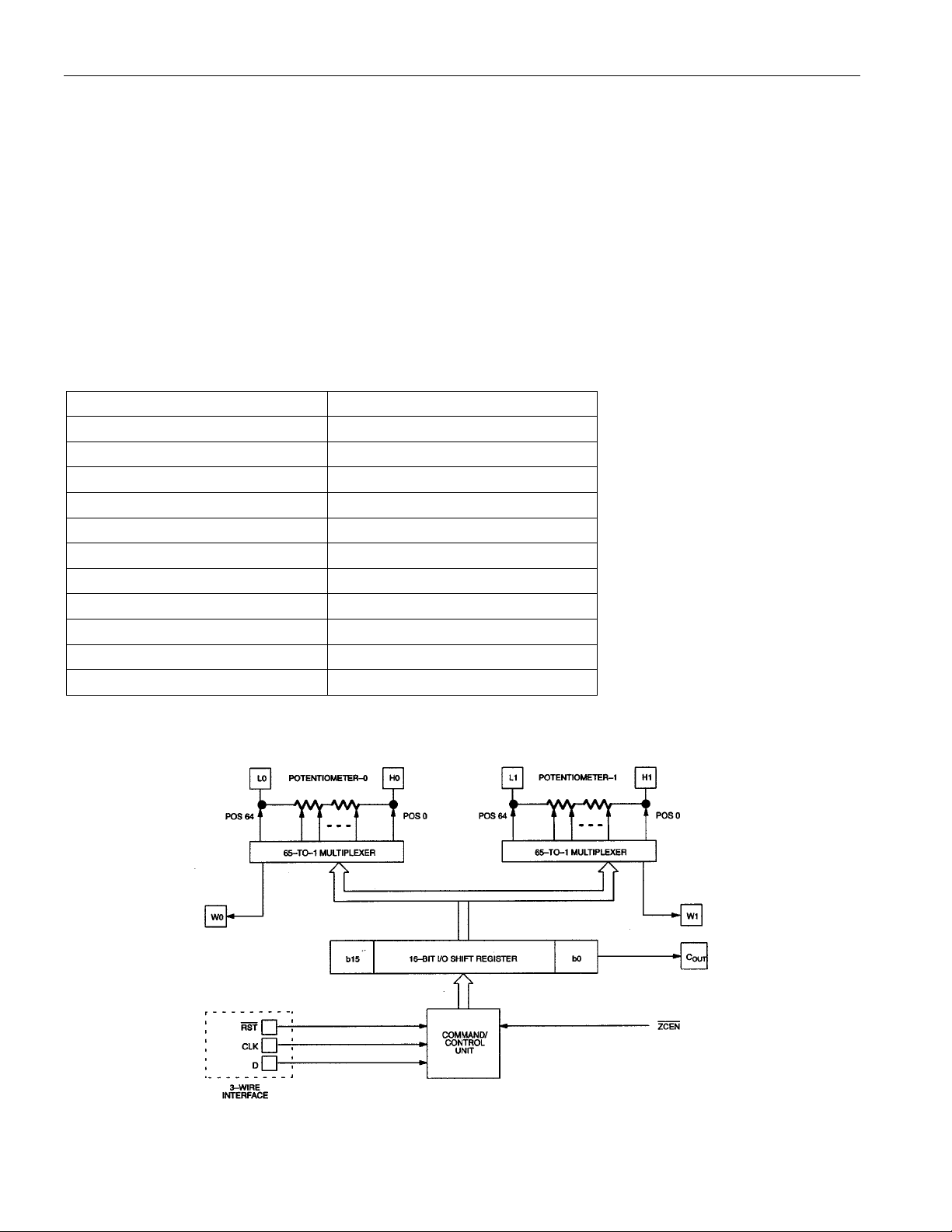
Figure 1 presents a block diagram of the DS1801. As shown, the inputs from the 3-wire serial interface
drive a command/control unit. The command/control unit interprets these inputs for control of the two
potentiometers.
On power-up, the serial port is stable and active within 10 microseconds. The wiper position on power-up
will be at position 63, the low end of the potentiometer. Position 64 is the mute level.
RESISTANCE CHARACTERISTICS Table 1
POSITION OUTPUT LEVEL (dB)
00
1-1
2-2
3-3
4-4
5-5
63 -63
64(mute) <-90
DS1801 BLOCK DIAGRAM Figure 1
2 of 10
Page 3
DS1801
3-WIRE SERIAL INTERFACE CONTROL
Communication and control of the DS1801 is accomplished through a 3-wire serial port interface that
drives an internal control logic unit. The 3-wire serial interface is designed for microprocessor or
microcontroller applications. The interface consists of three input signals which include
RST , CLK and
D.
The
RST control signal is used to enable 3-wire serial port write operations. The CLK terminal is a clock
signal input that provides synchronization for data I/O while the D signal input serves to transfer
potentiometer wiper position settings to the device.
As shown in Figure 3, a 3-wire serial port operation begins with a transition of the RST signal input to a
high state. Once the 3-wire port has been activated, data is clocked into the part on the low to high
transition of the CLK signal input. Data input via the D line is transferred in the order of the desired
potentiometer-0 value followed by the potentiometer-1 value.
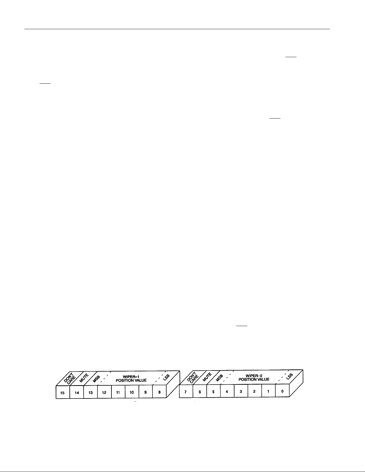
The DS1801 contains two 65-position potentiometers whose wiper positions are set by an 8-bit value.
These two 8-bit values are written to the 16-bit I/O shift register which is used to store wiper position
during powered conditions. Because the potentiometer has 65-positions, only 7 bits of data are needed to
set wiper position. A detailed diagram of the 16-bit I/O shift register is shown in Figure 2. Bits 0 through
7 are reserved for the potentiometer-0 control while bits 8 through 15 are reserved for control of
potentiometer-1.
Bits 0 through 5 are used for actual wiper positioning of potentiometer-0. Bit 6 is used to mute
potentiometer-0. If this bit has value 1, the potentiometer-0 wiper will be connected to the low end of the
resistive array the mute position. The value of bit 7 is a “don’t care” and will not affect operation of the
DS1801 or potentiometer-0.
Bits 8 through 13 are used for wiper positioning of potentiometer-1. Bit 14 is used for muting of the
potentiometer-1 wiper output. Bit 15, like bit 7, is a “don’t care” and will not affect operation of the
DS1801.
Data for the DS1801 is transmitted LSB first starting with bit 0. A complete transmission of 16 bits of
data is required to insure proper setting of each potentiometer’s wiper. An incomplete transmission may
result in undesired wiper settings.
Once the complete 16 bits of information has been transmitted and the RST signal input transitions to a
low state, the new wiper positions are loaded into the part.
16-BIT I/O SHIFT REGISTER Figure 2
3 of 10
Page 4

TIMING DIAGRAMS Figure 3
DS1801
4 of 10
Page 5

DS1801
CASCADE OPERATION
A feature of the DS1801 is the ability to control multiple devices from a single processor. Multiple
DS1801s can be linked or daisy-chained as shown in Figure 4. As a data bit is entered into the I/O shift
register of the DS1801, bit 0 of the I/O shift register will appear at the C
of 50 nanoseconds.
output after a maximum delay
OUT
The C
output of the DS1801 can be used to drive the D input of another DS1801. When connecting
OUT
multiple devices, the total number of bits sent is always 16 times the number of DS1801s in the daisy
chain.
An optional feedback resistor can be placed between the C OUT terminal of the last device and the D input
of the first DS1801 thus allowing the controlling processor to read as well as write data or circularly
clock data through the daisy chain. The value of the feedback or isolation resistor should be in the range
from 2 to 10 kohms.
When reading data via the C
When RST is driven high, bit 0 is present on the C
pin and isolation resistor, the D line is left floating by the reading device.
OUT
pin, which is fed back to the input D pin through
OUT
the isolation resistor. When the CLK input transitions low to high, bit 0 is loaded into the first position of
the I/O shift register and bit 1 becomes present on C
and D of the next device. After 16 bits (or 16
OUT
times the number of DS1801s in the daisy chain), the data has shifted completely around and back to its
original position. When RST transitions to the low state to end data transfer, the value (the same as before
the read occurred) is loaded into wiper-0 and wiper-1.
CASCADING MULTIPLE DEVICES Figure 4
Zero-Crossing Detection
The DS1801 provides a zero-crossing detection capability that minimizes any audible noise that may
result from sizable discrete wiper transitions when using the part in audio applications. The zero-crossing
detect feature allows independent wiper changes only when the two terminals of the potentiometer have
equal potentials and are within a 50 ms time window from the fall of the RST signal. If at 50 ms the
DS1801 has not detected a zero-crossing, the wiper position of the potentiometer(s) will change
regardless of the state of the input signal. Zero-crossing detection is activated when the ZCEN input level
is in a low-state. When high, the ZCEN input deactivates both the 50 ms time requirement and zero
detection crossing.
5 of 10
Page 6

TYPICAL SUPPLY CURRENT VS. SERIAL CLOCK RATE Figure 5
DS1801
6 of 10
Page 7

DS1801
ABSOLUTE MAXIMUM RATINGS*
Voltage on Any Pin Relative to Ground -0.7V to +7.0V
Operating Temperature -40° to +85°C; industrial
Storage Temperature -55°C to +125°C
Soldering Temperature 260°C for 10 seconds
* This is a stress rating only and functional operation of the device at these or any other conditions above
those indicated in the operation sections of this specification is not implied. Exposure to absolute
maximum rating conditions for extended periods of time may affect reliability.
RECOMMENDED DC OPERATING CONDITIONS (-40°C to +85°C)
PARAMETER SYMBOL MIN TYP MAX UNITS NOTES
Supply Voltage V
Input Logic 1 V
Input Logic 0 V
CC
IH
IL
+2.7 5.5 V
+2.0 VCC+0.5 V 1,2
-0.5 +.08 V 1,2
Resistor Inputs L,H,W GND-0.5 VCC+0.5 V 2
Analog Ground AGND GND-0.5 GND+0.5 V 10
DC ELECTRICAL CHARACTERISTICS (-40°C to +85°C; VCC=2.7V to 5.5V)
PARAMETER SYMBOL MIN TYP MAX UNITS NOTES
Supply Current I
Input Leakage I
Wiper Resistance R
Wiper Current I
Logic 1 Output Current @2.4V I
Logic 0 Output Current @0.4V I
CC
LI
W
W
OH
OL
µA
-1 +1
400
µA
Ω
1mA
-.4 mA 2
2mA2
9
Standby Current: 3 Volts
5 Volts
7 of 10
12
20
30
50
µA
µA
11
Page 8

DS1801
ANALOG RESISTOR CHARACTERISTICS (-40°C to +85°C; VCC=2.7V to 5.5V)
PARAMETER SYMBOL MIN TYP MAX UNITS NOTES
End to End Resistor Tolerance -20 +20 % 13
Absolute Tolerance
Interchannel Matching
-1 +1 dB
-0.5
+0.5
dB
8
4
Tap-to-Tap Tolerance -0.25 +0.25 dB 5,12
-3 dB Cutoff Frequency f
CUTOFF
Temperature Coefficient 750 ppm/°
Total Harmonic Distortion
(VIN=1V
, 1 kHz, Tap= -6
RMS
THD 0.002 % 12
700 kHz
°C
°°
dB)
Output Noise (20 Hz to 20 kHz,
Grounded Input, Tap= -6 dB)
Digital Feedthrough
2.2
µV
RMS
-90 dB 12
(20 Hz to 20 kHz, Tap= -6 dB)
Interchannel Isolation (20
-100 dB 12
Hz to 20kHz, Tap= -6 dB)
Mute Control Active Mute -90 dB
CAPACITANCE (-40°C to +85°C; VCC=2.7V to 5.5V)
PARAMETER SYMBOL MIN TYP MAX UNITS NOTES
Input Capacitance C
Output Capacitance C
IN
OUT
5pF 6
7pF 6
8 of 10
Page 9

DS1801
AC ELECTRICAL CHARACTERISTICS (-40°C to +85°C; VCC=2.7V to 5.5V)
PARAMETER SYMBOL MIN TYP MAX UNITS NOTES
CLK Frequency f
Width of CLK Pulse t
Data Setup Time t
Data Hold Time t
Propagation Delay Time
CLK
CH
DC
CDH
t
PLH
Low to High Level
Clock to Output
Propagation Delay Time
t
PLH
Low to High Level
t
t
HLT
t
RLT
CC
CR
RST High to Clock Input High
RST Low to Clock Input High
CLK Rise Time t
RST Inactive
NOTES:
1. All voltages are referenced to ground.
DC 10 MHz 7
50 ns 7
30 ns 7
10 ns 7
50 ns 7
50 ns 7
50 ns 7
50 ns 7
60 ns 7
200 ns 7
2. Valid for VCC = 2V only.
3. Capacitance values apply at 25°C.
4. Inter-channel matching is used to determine the relative voltage difference in dB between the same
tap position on each potentiometer. The DS1801 is specified for ±0.5 dB inter-channel matching.
5. Tap-to-tap tolerance is used to determine the change in voltage between successive tap positions. The
DS1801 is specified for ±0.25 dB tap-to-tap tolerance.
6. Typical values are for TA=25°C and nominal supply voltage.
7. See Figure 3.
8. Absolute tolerance is used to determine measured wiper voltage vs. expected wiper voltage as
determined by wiper position. The DS1801 is bounded by a ±1 dB absolute tolerance.
9. Maximum current specifications are based on clock rate and active zero-crossing detection. See
Figure 5 for clock rate vs. current specification.
10. See Figure 7.
11. Standby current levels apply when all inputs are driven to appropriate supply levels.
12. These parameters are characterized and not 100% tested.
13. Valid at 25° C only.
9 of 10
Page 10

DIGITAL OUTPUT LOAD Figure 6
INTERNAL GROUND CONNECTIONS Figure 7
DS1801
NOTE:
GND and AGND must be tied to the same voltage level.
DS1801 ORDERING INFORMATION
ORDERING
INFORMATION
DS1801 14L DIP -40°C to +85°C
DS1801E 14L TSSOP (173-mil) -40°C to +85°C
DS1801S 16L SOIC (300-mil) -40°C to +85°C
PACKAGE OPERATING
10 of 10
VERSION
TEMPERATURE
45 kΩ
45 kΩ
45 kΩ
 Loading...