

Page 1
DS1800
PRODUCT PREVIEW
DS1800
Dual Inverting Log Gain/Attenuator
FEATURES
• Ultra–low power consumption
• Operates from 3V or 5V supplies
• Two digitally controlled, 128–position potentiometers
including mute
• Logarithmic Gain Characteristics
• Zero–crossing detection circuitry eliminates noise
caused by discrete wiper position changes
• Two Control Interfaces
– 3–wire serial CPU control
– Push–button control
• 20–pin DIP (300 Mil), 20–pin SOIC (300 Mil), and
20–pin (173 Mil) TSSOP packaging available
• Operating Temperature:
– Commercial: 0°C to 70°C
– Industrial: –40°C to 85°C
• Software and hardware mute
• Resistance Available: 53KΩ
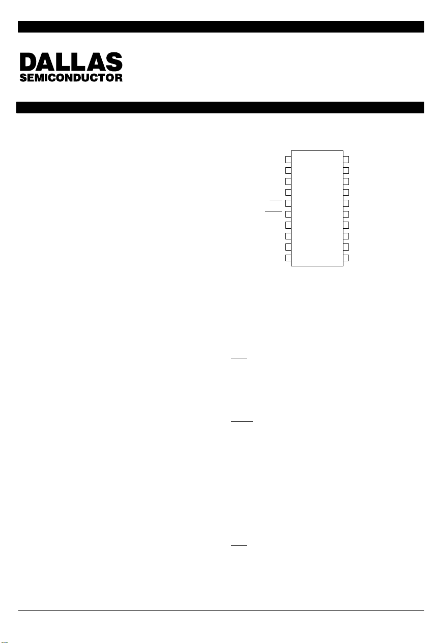
PIN ASSIGNMENT
GND
1
C
2
OUT
3
CLK
4
D
5
RST
ZCEN
MODE
OUT0
6
7
8
W0
9
10
IN0
20–PIN DIP (300 MIL)
20–PIN SOIC (300 MIL)
20–PIN TSSOP
20
V
CC
19
P1G
18
P1A
17
P0G
16
P0A
15
MUTE
14
AGND
13
IN1
12
OUT1
11
W1
PIN DESCRIPTION
OUT0,OUT1 – Low–end of resistor
IN0, IN1 – High–end of resistor
W0,W1 – Wiper Terminal
V
CC
RST – Serial Port Reset Input
CLK – Serial Port Clock Input
D – Serial Port Data Input
C
OUT
P0G,P1G – Gain Input Pot Controls
P0A,P1A – Attenuation Input Pot Controls
ZCEN – Zero–Crossing Detect Input
MUTE – Hardware Mute Control Input
AGND – Analog Ground
GND – Ground
– 3V or 5V Power Supply Input
– Cascade Data Output
DESCRIPTION
The DS1800 is a dual audio–taper potentiometer
designed specifically for use in the feedback path of the
inverting configuration of an operational amplifier (see
Figure 2). In this configuration, the DS1800 provides a
relationship of –20log(RF/RI) giving a gain/attenu-
V
O/VI
ation range covering +20 dB to –63 dB. Each potentiometer has a total of 129 positions including mute. The
DS1800 provides five areas of resolution which include
0.25 dB per step from +20 dB to +3 dB, 0.5 dB per step
from +3 dB to –12 dB, 1 dB from –12 dB to –27 dB, and
Copyright 1995 by Dallas Semiconductor Corporation.
All Rights Reserved. For important information regarding
patents and other intellectual property rights, please refer to
Dallas Semiconductor data books.
from –27 dB to –47 dB; 2 dB per step, and from –47 dB to
–63 dB; 4 dB per step. The mute position provides 100
dB of attenuation.
The DS1800 has two control interfaces (see Figure 1).
The first is a 3–wire serial CPU interface consisting of
RST
, CLK, and D. The second interface is a contact–
closure interface, allowing easy push–button control
without the need for external debounce or timing circuitry. The device also provides for software muting (via
072095 1/13
Page 2

DS1800
CPU) or hardware muting (MUTE control input). The
hardware mute is a toggle type which returns the wiper
positions to their prior states. Additional information on
CPU and push–button control is described under the
section entitled “OPERATION”.
The DS1800 is available in 20–pin DIPs, SOICs, and
TSSOPs. One standard resistance grade of 53KΩ is
available for the device.
OPERATION
The DS1800 provides two 129–position 45KΩ potentiometers. These potentiometers are specifically
designed to operate in the configuration shown in Figure
2. Under this configuration the V0/VI relationship provides the gain/attenuation function of –20log(R
F/RI
over a range of +20 dB to –63 dB. This function is illustrated in Figure 3 as a graph of gain/attenuation versus
position. Figure 4 provides the relationship between R
and RI as a function of position.
The DS1800 has a total of 129 positions including a
mute position. Five areas of resolution are provided
over the gain/attenuation range and are illustrated in
Figure 3. From position 0 to position 68, a resolution of
0.25 dB per step is attained covering a gain/attenuation
range of +20 dB to +3 dB. From position 68 to position
98, 0.5 dB per step of resolution is attained covering +3
dB to –12 dB of gain/attenuation. Positions 98 to 113
have 1 dB per step resolution and cover a gain/attenuation range of –12 to –27 dB. Positions 113 to 123 provide 2 dB per step and cover a gain/attenuation range of
–27 dB to –47 dB. Positions 123 to 127 provide 4 dB per
step and cover a gain/attenuation range of –47 dB to 63
dB. Position 128 is the mute position and typically provides 100 dB of attenuation.
PIN DESCRIPTIONS
The DS1800 has a total of 20 pins which provide various
functions for the device. This section provides a
description of each pin’s operation.
V
– Power Supply Voltage Input. The DS1800 will
CC
support 3V or 5V power supply operation.
GND – Ground. The DS1800 has two ground pins. The
GND supports the digital ground for the device.
AGND – Analog Ground. The DS1800 has two ground
pins. The AGND supports analog ground for the device.
IN0, IN1 – Input terminals for the two respective potentiometers as shown in Figure 2. These terminals should
be connected to the analog signal,VI, to provide the
gain/attenuation characteristics stated. These terminals are referenced as INx in the Figure 2 drawing.
OUT0, OUT1 – Analog Outputs. These pins should be
connected to the output terminal of the operational
amplifier as shown in Figure 2. These inputs are referenced as OUTx in the Figure 2 drawing.
W0, W1 – Wiper T erminals. The wiper terminals of each
pot are connected to the inverting terminal of the operational amplifier. The position of the wiper terminal is
selected either through CPU control or push–button
control.
)
P0A, P1A – Attenuation Push–button Inputs. These
push–button inputs are used to control wiper position of
F
the part . Activity on these inputs will cause the position
of the wiper to move towards the OUT0, and OUT1 terminals, respectively .
P0G, P1G – Gain Push–button Inputs. These push–
button inputs control wiper position and are used to
move the position of the wiper towards the IN0 and IN1
terminals, respectively .
RST
– Serial Port Reset. The RST input deactivates the
3–wire serial interface. This input is active when in the
low–state. All 3–wire communications must take place
when this input is in a high state.
CLK – Serial Clock Input. The CLK input is the positive–
edge clock signal input used for 3–wire timing synchronization.
D – Serial Data Input. The D input is used to input serial
data for wiper position changes.
C
– Serial Cascade Output. The C
OUT
OUT
signal used to read the contents of the current settings
of the wiper positions. As data is clocked into the D
input, data corresponding to the wipers are shifted out of
OUT
pin.
the C
MODE – Push–button Debounce Control. The MODE
pin is used to choose between a fast and slow mode of
push–button debouncing. When in a high state, push–
button debounce is slow. When in a low–state, push–
is an output
072095 2/13
Page 3

DS1800
button debounce is faster. These timing differences are
discussed in the section entitled “Push–button Interface Control”. The state of this pin is determined only at
device power–up.
POWER–UP CONDITIONS
The position of the wipers of the DS1800 on power up
are internally set to position 127, which is the last position before mute. The user then has the responsibility of
changing the wiper position to the desired attenuation/
gain levels.
Additionally , the serial port is stable and active within 10
microseconds. The contact closure control interface
inputs are active after 50 ms.
INTERFACE CONTROL OPTIONS
Control of the DS1800 is provided via two types of interface ports. A 3–wire CPU control interface allows the
exact wiper positions of the potentiometers to be written
using two 8–bit words. A cascade output, C
OUT
, is provided when controlling multiple devices via one CPU or
when reading the wiper positions of each potentiometer .
The second interface is a contact closure interface that
allows push–buttons to control movement of the wiper
positions. Under push–button control no external
debounce or timing circuitry is needed. A block diagram
of the DS1800 is shown in Figure 1.
3–WIRE SERIAL INTERFACE CONTROL
CPU control of the DS1800 is accomplished using the
3–Wire serial port of the device. This interface drives an
internal control logic unit. Direct wiper positioning is
accomplished by using this port which consist of three
input signals: RST, CLK, and D.
The RST
port write operations. The CLK terminal is an input that
provides synchronization for data I/O. Data is input bit
by bit via the D input signal pin.
The 3–Wire serial timing diagrams are provided in Figure 5. Serial port operation or activity begins with the
transition of the RST
state. Once activated, data is clocked into the part on
the low to high transition of the CLK signal input. Data
input via the D terminal is transferred in order of the
control signal is used to enable 3–wire serial
signal from a low–state to a high–
desired potentiometer–0 wiper value, followed by the
potentiometer–1 wiper position value.
Two 8–bit values are used to store wiper position for
each potentiometer during powered conditions. These
8–bit values are written to a 16–bit I/O shift register. A
detailed diagram of the 16–bit I/O shift register is shown
in Figure 6.
Bits 0 through 7 are reserved for the positioning of
wiper–0 while bits 8 through 15 are reserved for control
of wiper–1. Bits 0 through 6 are used for actual wiper
positioning of potentiometer–0. Bit 7 is used to mute
potentiometer–0. If this bit is set to a “1”, the potentiometer–0 wiper will be connected to the OUT0 end of the
resistor array regardless of the settings of bits 0 through
6.
Bits 8 through 15 are used for positioning the wiper of
potentiometer–1. Bits 8 through 14 control wiper position on the resistor array. Bit 15 is used for muting potentiometer–1. Bit 15, like bit 7, when set to “1” will mute
potentiometer 1, regardless of the settings of bits 8
through 14.
Data is transmitted LSB first starting with bit–0. A complete transmission of 16 bits of data is required to insure
proper setting of each potentiometer’s wiper. An incomplete transmission may result in undesired wiper settings.
Once the 16 bits of information has been transmitted
and the RST
signal input transitions to a low–state, the
new wiper positions are loaded into the part.
PUSH–BUTTON INTERFACE CONTROL
The DS1800 can be configured to operate from contact
closure or push–button inputs. The push–button inputs
consist of signals P0A, P0G, P1A, P1G and MUTE.
P0A and P0G allow attenuation and gain control of the
input signal to potentiometer–0, while P1A and P1G
provide the same control for potentiometer–1. The
MUTE input provides a toggle control for muting the
potentiometers via pushbutton.
The P0A and P1A control inputs, based on the recommended circuit configuration, are used to attenuate the
incoming signal by moving the wiper position towards
the OUTx terminals. The P0G and P1G control inputs
072095 3/13
Page 4

DS1800
provide the opposite function; positioning the wiper(s)
closer to the INx terminals, thus providing gain.
Each of these control inputs are internally pulled–up via
a 50KΩ resistance. Additionally, these inputs require no
external components for debouncing or timing which
are provided internal to the part.
Contact closure is defined as the transition from a high
level to a low level on these input terminals. The
DS1800 interprets input pulse widths as the means of
controlling wiper movement. A single pulse input over
the PxA or PxG input terminals will cause the wiper to
move one position. A transition from high to low on
these inputs is considered the beginning of pulse activity or contact closure. The DS1800 has two timing
modes for controlling the speed at which pushbuttons
will operate. These modes are termed fast mode operation and slow mode operation.
In slow mode operation, a single pulse is defined as
being greater than 1 ms but lasting no longer than 0.8
seconds. Correspondingly, in fast mode operation, a
single pulse is defined as being greater than 50 µs but
lasting no longer than 0.8 second.
Repetitive pulsed inputs can be used to step through
each resistive position of the device in a relatively fast
manner. The timing requirements for repetitive pulsed
inputs is that pulses must be separated by a minimum
time of 1 ms for slow mode operation and 50 µs for fast
mode operation.
Pulse inputs lasting longer than 0.8 seconds will cause
the wiper to move one position every 25 ms seconds
after the initial 0.8 second hold time. This is true regardless of the mode input. The total time required to transcend the entire potentiometer using a continuous input
pulse is given by the following formula:
0.8(seconds) + 127 x 25 ms = 3.975(seconds)
SLOW MODE AND FAST MODE OPERATION
Pushbutton operation, as mentioned. can be operated
at two distinct speeds or modes; fast and slow. The
mode or speed of pushbutton debounce is determined
at device power–up by the state of the MODE pin. When
MODE powers to a high–state, pushbutton debounce
timing will operate at the slow mode rate. When powered and in the low–state, debounce timing operates at
the fast rate. Timing specifications for pushbutton
operation can be found in the AC Electrical Specification
Table for pushbutton operation. Timing diagrams for
push–button operation can be found in Figure 7.
ZERO CROSSING DETECTION
The DS1800 provides a zero–crossing detection capability when using the 3–Wire serial interface. Zero–
crossing detection provides a means for minimizing
unwanted audible noise that may result from sizable discrete wiper transitions when using the part in audio
applications. The zero crossing detect feature allows
independent wiper changes only when the two terminals of the potentiometer(s) have equal potentials and
within a 50 ms time window from the fall of the RST
signal. If at 50 ms the DS1800 has not detected a zero
crossing, the wiper position of the potentiometer(s) will
change regardless of the state of the input signal. Zero–
crossing detection is activated when the ZCEN input is
in a low–state. When high, the ZCEN
input deactivates
both the 50 ms time requirement and zero–detection
crossing.
Zero crossing detection is also available when using the
part in push–button operation. When a push–button is
activated, the part will change wiper position during the
first detected zero–crossing or at the end of a 50 ms time
window.
When operating in push–button operation with a continuous input pulse, the wiper position will change once
during the initial 0.8 second time period. This change is
dictated by a detected zero–crossing or 50 ms time window. Subsequent changes when operating with a continuous input pulse occur on 25 ms time intervals and
are dependent on zero crossings or 50 ms time–outs.
MUTE CONTROL
The DS1800 provides a mute control feature which can
be accessed by the user through hardware or software.
Hardware control of the device is achieved through the
MUTE input pin. This pin is internally pulled up through
a 50K resistor and functions like the PxG and PxA pushbutton controls. When this input is driven low, the wiper
outputs of both potentiometers will be internally connected to the OUTx terminal of their respective potentiometers. This input performs as a toggle input, with the
first activity on this pin connecting the wiper terminals to
the OUTx terminals (position 128) of the potentiometer.
The next input activity on this pin will return the wiper
position to the previous state before muting occurred.
072095 4/13
Page 5

DS1800
Also, if operating in push–button mode, MUTE will be
deactivated if an input is received over any push–button
input. This input, like the push–button inputs, is internally debounced and requires no external circuitry.
When the device powers up, the first activity on the mute
pin will move the wipers to position 128 or the OUTx end
of the potentiometer(s).
Software muting was discussed in the 3–wire serial control section. Bits 7 and 15 are reserved for muting each
respective potentiometer. If these bits have value “1”,
the wiper positions of the pot will be transferred to the
mute position. Unlike hardware mute control, software
muting allows the user individual control of each potentiometer. Additionally, the software mute requires that
the complete wiper position setting be rewritten to
establish a non muted position. Note that bits 7 and 15
of the I/O shift register must have value “0” to release the
software mute position.
CASCADE OPERATION
A feature of the DS1800 is the ability to control multiple
devices from a single processor. Multiple DS1800’s can
be linked or daisy chained as shown in Figure 8. As a
data bit is entered into the I/O shift register of the
DS1800, a data bit will appear at the C
maximum delay of 50 nanoseconds.
output after a
OUT
The C
output of the DS1800 can be used to drive the
OUT
D input of another DS1800. When connecting multiple
devices, the total number of bits sent is always 16 times
the number of DS1800’s is the daisy chain.
An optional feedback resistor can be placed between
the C
terminal of the last device and the D input of
OUT
the first DS1800, thus allowing the controlling processor
to circularly clock data through the daisy chain. The
value of the feedback or isolation resistor should be in
the range from 2K to 20KΩ.
When reading data via the C
pin and the isolation
OUT
resistor, the D input is left floating by the reading device.
When RST is driven high, bit–0 is present on the C
OUT
pin, which is fed back to the D pin through the isolation
resistor. When the CLK input transitions low to high,
bit–0 is loaded into the first position of the I/O shift register and bit 1 becomes present on C
and D of the next
OUT
device. After 16 bits (or 16 times the number of
DS1800s in the daisy chain), the data has shifted completely around and back to its original position. When
transitions to the low state to end data transfer, the
RST
value (the same as before the read occurred is loaded
into the wiper–0 and wiper–1 registers.
072095 5/13
Page 6

DS1800
ABSOLUTE MAXIMUM RATINGS*
Voltage on Any Pin Relative to Ground –1.0V to +7.0V
Operating Temperature 0°C to 70°C; commercial
–40°C to +85°C; industrial
Storage Temperature –55°C to 125°C
Soldering Temperature 260°C for 10 seconds
* This is a stress rating only and functional operation of the device at these or any other conditions above
those indicated in the operation sections of this specification is not implied. Exposure to absolute maximum rating conditions for extended periods of time may af fect reliability.
RECOMMENDED DC OPERATING CONDITIONS (–40°C to +85°C)
PARAMETER SYMBOL MIN TYP MAX UNITS NOTES
Supply Voltage V
Input Logic 1 V
Input Logic 0 V
CC
IH
IL
2.7 5.5 V 1
2.0 VCC+0.5 V 1, 2
–0.5 +0.8 V 1, 2
Analog Ground AGND GND–0.5 GND+0.5 14
Resistor Inputs L,H,W GND–0.5 GND+0.5 V 1
DC ELECTRICAL CHARACTERISTICS (–40°C to +85°C; VCC=2.7V to 5.5V)
PARAMETER SYMBOL MIN TYP MAX UNITS NOTES
Supply Current I
Input Leakage I
Wiper Resistance R
Wiper Current I
Logic 1 Output Current @ 2.4V I
Logic 0 Output Current @ 0.4V I
Standby Current: 3 Volts
I
5 Volts
Power Up Time t
CC
LI
W
W
OH
OL
STBY
PU
–1 +1 µA
400 1000 Ω
–1 mA
12
20
50 ms 8
2000 µA 10
1 mA
4 mA
40
µA
µA
12
072095 6/13
Page 7

DS1800
ANALOG RESISTOR CHARACTERISTICS (–40°C to +85°C; VCC=2.7V to 5.5V)
PARAMETER SYMBOL MIN TYP MAX UNITS NOTES
Total Resistance 53 KΩ
End–to–End Resistor Tolerance –20 +20 %
Absolute Tolerance –0.5
–1.0
Tap–to–Tap Tolerance –0.5 +0.5 dB 7
Interchannel Matching –0.25
–0.5
–3 dB Cutoff Frequency f
cutoff
1 MHz 13
T emperature Coef ficient 650 ppm/°C
Total Harmonic Distortion
=1Vrms, 20 Hz to 20 KHz,
(V
IN
Tap=0 dB)
Output Noise (20 Hz to 20 KHz,
THD 0.002 % 13
2.2 µVrms 13
Grounded Input, Tap=0 dB)
Digital Feedthrough (20 Hz to 20
–90 dB 13
KHz, Tap=0 dB)
Interchannel Isolation (1 KHz,
–100 dB 13
Tap=0 dB)
Mute Control Active MUTE –100 dB
+0.5
+1.0
+0.25
+0.5
dB
dB
dB
dB
9
6
CAPACITANCE (–40°C to +85°C; VCC=2.7V to 5.5V)
PARAMETER SYMBOL MIN TYP MAX UNITS NOTES
Input Capacitance C
Output Capacitance C
IN
OUT
5 pF
7 pF
072095 7/13
Page 8

DS1800
AC ELECTRICAL CHARACTERISTICS (–40°C to +85°C; VCC=2.7V to 5.5V)
PARAMETER SYMBOL MIN TYP MAX UNITS NOTES
CLK Frequency f
Width of CLK Pulse t
Data Setup Time t
Data Hold Time t
Propagation Delay Time
Low to High Level
CLK
CH
DC
CDH
t
PLH
DC 10 MHz
50 ns
30 ns
10 ns
50 ns
High to Low Level
RST High to Clock Input High t
RST Low from Clock Input High t
CLK Rise Time t
RST Inactive t
CC
HLT
CB
BLT
50 ns
50 ns
50 ns
200 ns
AC ELECTRICAL CHARACTERISTICS
PUSHBUTTON INPUTS (–40°C to +85°C; V
PARAMETER SYMBOL MIN TYP MAX UNITS NOTES
Single Pulse Input
Slow Mode
Fast Mode
Repetitive Input Pulse High Time
Slow Mode
Fast Mode
Continuous Input Pulse t
t
CPW
t
HPW
CCP
1
800 ms
50
1
800 ms
50
0.8 DC s 3, 5, 11
=2.7V to 5.5V)
CC
µs
µs
3, 5, 11
3, 5, 11
NOTES:
1. All voltages are referenced to ground
2. Valid for V
3. Both PxA and PxG inputs are internally pulled up with a 50KΩ resistance.
4. Capacitance values apply at 25°C.
5. Input pulse width is the minimum time required for an input to cause an increment or decrement of wiper position. If the PxA or PxG inputs are held active for longer than 0.8 seconds, subsequent increments or decrements will occur at intervals of 25 ms. Timing tolerances for pushbutton control are specified at 35%.
6. Inter–Channel Matching is used to determine the relative voltage difference in dB between the same position
on each potentiometer. The DS1800 is specified for ±0.25 dB inter channel matching from position 0 to position 112 (+20 dB to –27 dB) and ±0.5 dB from position 113 to position 127.
7. Tap–to–Tap tolerance is used to determine the change in voltage between successive tap positions. The
DS1800 is specified for ±0.5 dB tap–to–tap tolerance. From position 0 to position 112 (+20 dB to –27 dB).
From position 113 to position 127, the DS1800 is specified for ± 1 dB tap–to–tap tolerance.
072095 8/13
= 5V only.
CC
Page 9

DS1800
8. Power–up time is the time for all push–button inputs to be stable and active once power has reached a valid
level, 2.7V min.
9. Absolute tolerance is used to determine wiper voltage versus expected wiper voltage as determined by wiper
position. The DS1800 is bounded by a ±0.5 dB absolute tolerance from position 0 to position 112 and ±1 dB
tolerance from position 113 to position 127.
10.Maximum current specifications are based on clock rate, active zero–crossing detection, and push–button
activation.
11. Valid for V
=3V or 5V.
CC
12.Standby current levels apply when all inputs are driven to appropriate supply levels.
13.These parameters are characterized and not 100% tested.
14.See Figure 9.
DS1800 BLOCK DIAGRAM Figure 1
IN1 OUT0 IN1 OUT1
POTENTIOMETER–0 POTENTIOMETER–1
POS–0 POS–128 POS–0 POS–128
129–TO–1 MULTIPLEXER 129–TO–1 MULTIPLEXER
W0 W1
RST
CLK
D
3–WIRE SERIAL
INTERFACE
WIPER–0 (8–BIT REGISTER) WIPER–1 (8–BIT REGISTER)
B0 B7 B8 B15
CONTROL
LOGIC
UNIT
P0G
P0A
PUSHBUTTON CONTROL
INPUTS
P1G
P1A
COUT
MODE
072095 9/13
Page 10

DS1800
RECOMMENDED CIRCUIT CONFIGURATION Figure 2
DS1800
V
I
R
R
I
F
Wx
OUTxINx
–
+
V
/2
CC
VO/VI GAIN/ATTENUATION VS. POSITION RELATIONSHIP Figure 3
GAIN/ATTENUATION VERSUS POSITION
V
O
GAIN (dB)
072095 10/13
POSITION
Page 11

RF/RI RELATIONSHIP VS. POSITION Figure 4
RF, RI VERSUS POSITION
RESISTANCE (ohms)
POSITION
DS1800
3–WIRE SERIAL TIMING DIAGRAM Figure 5
C
RST
CLK
OUT
t
CC
t
DC
D
FIRST DATA BIT
t
PLH
t
CDH
t
CH
SECOND DATA BIT
•••
•••
•••
t
RLT
t
HLT
072095 11/13
Page 12

DS1800
16–BIT I/O SHIFT REGISTER Figure 6
WIPER–1
POSITION VALUE
15 14 13 12 11 10 9 8 7 6543210
WIPER–0
POSITION VALUE
CONTACT CLOSURE TIMING DIAGRAMS Figure 7
(a) Single Pulse Inputs
t
CPW
V
IH
V
IL
(b) Repetitive Pulse Inputs
t
CPW
V
IH
V
IL
t
HPW
(c) Continuous Pulse Inputs
V
IH
V
IL
CASCADING OPERATION Figure 8
072095 12/13
DD DC
DS1800
C
OUT
#1
t
CCP
C
DS1800
#2
OUT
2K–20KΩ
(ISOLATION RESISTOR)
DS1800
#n
OUT
Page 13

DS1800
DIGITAL OUTPUT LOAD Figure 9
D.U.T.
680Ω
INTERNAL GROUND CONNECTIONS Figure 10
AGND GND
5V
1.1 KΩ
50 pF
100Ω (TYPICAL)
NOTE: GND and AGND must be tied to the same voltage level.
072095 13/13
 Loading...