

Page 1
r
www.dalsemi.com
PRELIMINARY
DS1775
SOT23-5 Digital Thermomete
and Thermostat
FEATURES
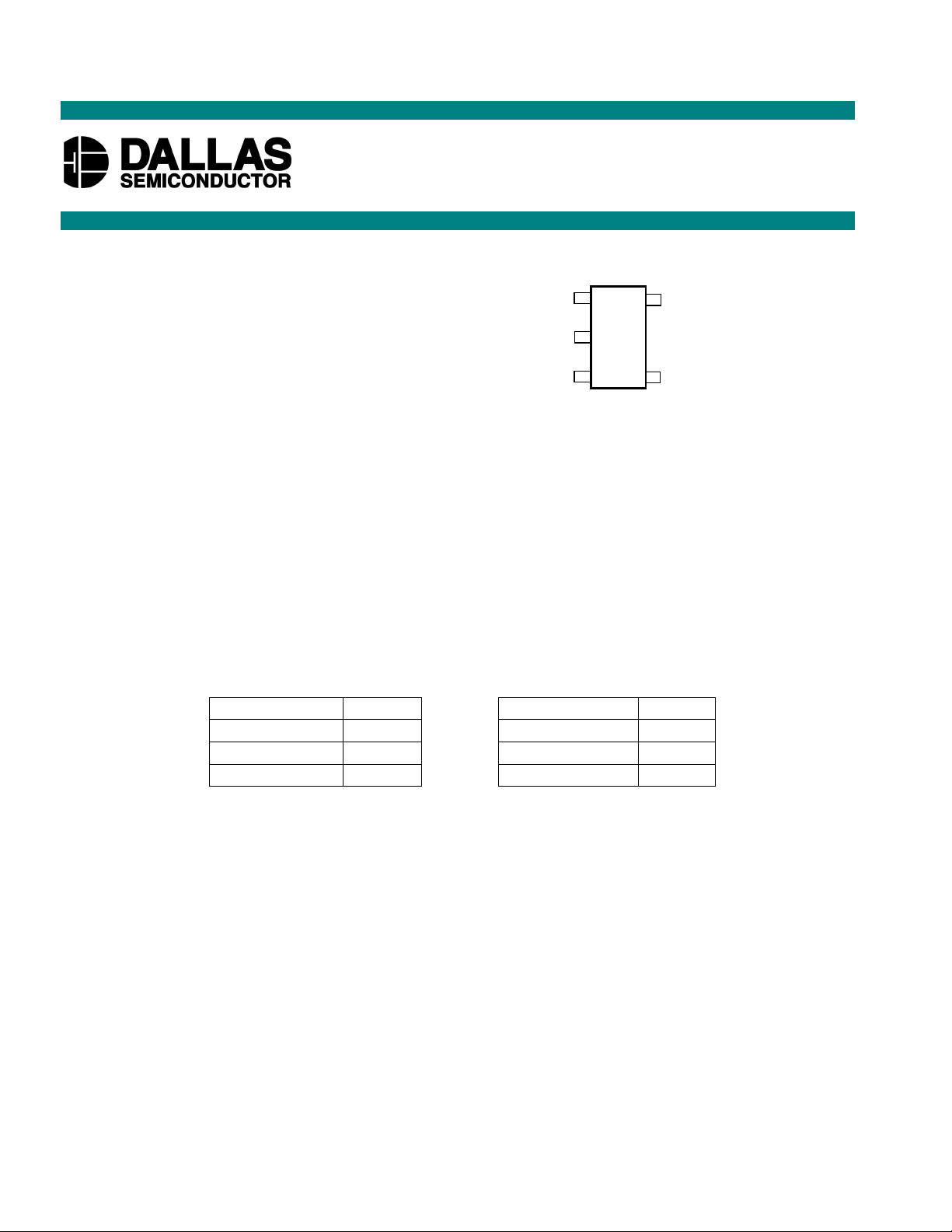
PIN ASSIGNMENT
Temperature measurements require no
external components
SCL
1
SDA
5
Measures temperatures from –55°C to
+125°C. Fahrenheit equivalent is –67°F to
257°F
GND
O.S.
2
3
V
4
DD
Thermometer accuracy is ±2.0°C
Thermometer resolution is configurable from
9 to 12 bits (0.5°C to 0.0625°C resolution)
DS1775R
SOT23-5
Thermostat settings are user definable
Data is read from/written to via a 2–wire
serial interface
Wide power supply range (2.7V – 5.5V)
Software compatible with DS75 2–Wire
Thermal Watchdog in thermometer mode
Space–conscious SOT23–5 package with
PIN DESCRIPTION
GND Ground
SCL 2–Wire Serial Clock
SDA 2–Wire Serial Data Input/Output
V
DD
O.S. Thermostat Output Signal
Power Supply Voltage
low thermal time constant
ORDERING INFORMATION
Part Number Address Part Number Address
DS1775R/TRL 000 DS1775R/TR4 100
DS1775R/TR1 001 DS1775R/TR5 101
DS1775R/TR2 010 DS1775R/TR6 110
DS1775R/TR3 011 DS1775R/TR7 111
* "R" denotes SOT 23-5 Package
DESCRIPTION
The DS1775 SOT23-5 Digital Thermometer and Thermostat provides temperature readings which
indicate the temperature of the device. Thermostat settings and temperature readings are all
communicated to/from the DS1775 over a simple 2–wire serial interface. No additional components are
required; the device is truly a “temperature–to–digital” converter.
For applications that require greater temperature resolution, the user can adjust the readout resolution
from 9 to 12 bits. This is particularly useful in applications where thermal runaway conditions must be
detected quickly.
The open–drain thermal alarm output, O.S., becomes active when the temperature of the device exceeds a
user–defined temperature TOS. The number of consecutive faults required to set O.S. active is
configurable by the user. The device can also be configured in the interrupt or comparator mode, to
customize the method which clears the fault condition.
As a digital thermometer, the DS1775 is software compatible with the DS75 2–Wire Thermal Watchdog.
1 of 13 122100
Page 2
DS1775
The DS1775 is assembled in a compact SOT23–5 package allowing for low–cost thermal
monitoring/control in space–constrained applications. The low thermal mass allows for time constants
previously only possible with thermistors.
Applications for the DS1775 include personal computers/servers/workstations, cellular telephones, office
equipment, or any thermally–sensitive system.
DETAILED PIN DESCRIPTION Table 1
PIN SYMBOL DESCRIPTION
PIN 1 SCL Clock input/output pin for 2-wire serial communication port. This input
should be tied to GND for standalone thermostat operation.
PIN 2 GND Ground pin.
PIN 3 O.S. Thermostat output Open-drain output becomes active when temperature
exceeds TOS. Device configuration defines means to clear over-temperature
state.
PIN 4 V
DD
Supply Voltage 2.7V – 5.5V input power pin.
PIN 5 SDA Data input/output pin for 2-wire serial communication port. In the standalone
thermostat mode, this input selects hysteresis.
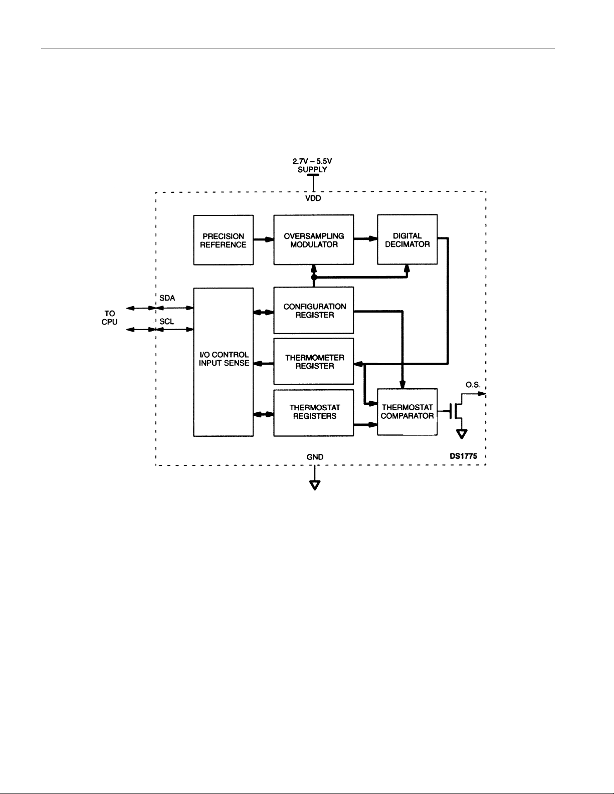
OVERVIEW
A block diagram of the DS1775 is shown in Figure 1. The DS1775 consists of five major components:
1. Precision temperature sensor
2. Analog–to–digital converter
3. 2–wire interface electronics
4. Data registers
5. Thermostat comparator
The factory–calibrated temperature sensor requires no external components. Upon power–up, the DS1775
begins temperature conversions with the default resolution of 9 bits (0.5°C resolution). The host can
periodically read the value in the temperature register, which contains the last completed conversion. As
conversions are performed in the background, reading the temperature register does not affect the
conversion in progress.
In power–sensitive applications the user can put the DS1775 into a shutdown mode, under which the
sensor will complete and store the conversion in progress and revert to a low–power standby state. In
applications where small incremental temperature changes are critical, the user can change the conversion
resolution from 9 bits to 10, 11, or 12. Each additional bit of resolution approximately doubles the
conversion time. This is accomplished by programming the configuration register. The configuration
register defines the conversion state, thermometer resolution/conversion time, active state of the
thermostat output, number of consecutive faults to trigger an alarm condition, and the method to
terminate an alarm condition.
The user can also program over–temperature (TOS) and under–temperature (T
thermostatic operation. The power–up state of T
temperature conversion is compared with the T
is 80°C and that for T
OS
and T
OS
setpoints. The DS1775 offers two modes for
HYST
is 75°C. The result of each
HYST
) setpoints for
HYST
temperature control, the comparator mode and the interrupt mode. This allows the user the flexibility to
customize the condition that would generate and clear a fault condition. Regardless of the mode chosen,
the O.S. output will become active only after the measured temperature exceeds the respective trippoint a
consecutive number of times; the number of consecutive conversions beyond the limit to generate an O.S.
2 of 13
Page 3
DS1775
is programmable. The power–up state of the DS1775 is in the comparator mode with a single fault
generating an active O.S.
Digital data is written to/read from the DS1775 via a 2–wire interface, and all communication is MSb
first.
DS1775 FUNCTIONAL BLOCK DIAGRAM Figure 1
OPERATION–Measuring Temperature
The core of DS1775 functionality is its direct–to–digital temperature sensor. The DS1775 measures
temperature through the use of an on–chip temperature measurement technique with an operating range
from –55°C to +125°C. Temperature conversions are initiated upon power–up, and the most recent result
is stored in the thermometer register. Conversions are performed continuously unless the user intervenes
by altering the configuration register to put the DS1775 into a shutdown mode. Regardless of the mode
used, the digital temperature can be retrieved from the temperature register by setting the pointer to that
location (00h, power–up default). The DS1775 power–up default has the sensor automatically performing
9–bit conversions continuously. Details on how to change the settings after power–up are contained in the
“OPERATION–Programming” section.
The resolution of the temperature conversion is configurable (9, 10, 11, or 12 bits), with 9–bit readings
the default state. This equates to a temperature resolution of 0.5°C, 0.25°C, 0.125°C, or 0.0625°C.
Following each conversion, thermal data is stored in the thermometer register in two’s complement
format; the information can be retrieved over the 2–wire interface with the device pointer set to the
temperature register. Table 2 describes the exact relationship of output data to measured temperature. The
3 of 13
Page 4
DS1775
table assumes the DS1775 is configured for 12–bit resolution; if the device is configured in a lower
resolution mode, those bits will contain zeros. The data is transmitted serially over the 2–wire serial
interface, MSb first. The MSb of the temperature register contains the “sign” (S) bit, denoting whether the
temperature is positive or negative. For Fahrenheit usage, a lookup table or conversion routine must be
used.
Temperature/Data Relationships Table 2
S262
5
MSb
-1
2
-2
2
-3
2
TEMP DIGITAL OUTPUT
4
2
(UNIT = °C)
-4
2
3
2
2
2
1
2
0
2
MSB
LSb
0000 LSB
DIGITAL OUTPUT (Hex)
(Binary)
+125°C
+25.0625°C
+10.125°C
+0.5°C
+0°C
-0.5°C
-10.125°C
-25.0625°C
-55°C
0111 1101 0000 0000 7D00h
0000 1010 0010 0000 1910h
0000 1010 0010 0000 0A20h
0000 0000 1000 0000 0080h
0000 0000 0000 0000 0000h
1111 1111 1000 0000 FF80h
1111 0101 1110 0000 F5E0h
1110 0110 1111 0000 E6F0h
1100 1001 0000 0000 C900h
OPERATION–Thermostat Control
In its comparator operating mode, the DS1775 functions as a thermostat with programmable hysteresis, as
shown in Figure 2. When the DS1775’s temperature meets or exceeds the value stored in the high
temperature trip register (TOS) a consecutive number of times, as defined by the configuration register, the
output becomes active and stays active until the first time that the temperature falls below the temperature
stored in the low temperature trigger register (T
obtained. The DS1775 powers up in the comparator mode with TOS=80°C and T
used as a standalone thermostat (no 2–wire interface required) with those setpoints.
). In this way, any amount of hysteresis may be
HYST
=75°C and can be
HYST
In the interrupt mode, the O.S. output will first become active following the programmed number of
consecutive conversions above T
shutdown mode or by reading any register (temperature, configuration, T
Following a clear, a subsequent fault can only occur if consecutive conversions fall below T
interrupt/clear process is thus cyclical (TOS, clear, T
of multiple consecutive T
violations will activate O.S., even if each fault is separated by a clearing
OS
function. The same situation applies to multiple consecutive T
. The fault can only be cleared by either setting the DS1775 in a
OS
HYST
4 of 13
, clear, TOS, clear, T
events.
HYST
, or T
OS
, clear, ...). Only the first
HYST
) on the device.
HYST
HYST
. This
Page 5

O.S. OUTPUT TRANSFER FUNCTION Figure 2
DS1775
Regardless of the mode chosen, the O.S. output is open–drain and the active state is set in the
configuration register. The power–up default is active low. Refer to the “OPERATION–Programming”
section for instructions in adjusting the thermostat setpoints, thermostat mode, and O.S. active state.
OPERATION–Programming
There are three areas of interest in programming the DS1775: the configuration register, the TOS register,
and the T
register. All programming is done via the 2–wire interface by setting the pointer to the
HYST
appropriate location. Table 3 illustrates the pointer settings for the four registers of the DS1775.
Pointer Register Structure Table 3
POINTER ACTIVE REGISTER
00h Temperature (default)
01h Configuration
02h T
03h T
The DS1775 will power up with the temperature register selected. If the host wishes to change the data
pointer it simply addresses the DS1775 in the write mode (R/ W =0), receives an acknowledge, and writes
the 8 bits that correspond to the new desired location. The last pointer location is always maintained so
that consecutive reads from the same register do not require the host to always provide a pointer address.
The only exception is at power–up, in which case the pointer will always be set to 00h, the temperature
HYST
OS
5 of 13
Page 6

DS1775
register. The pointer address must always proceed data in writing to a register, regardless of which
address is currently selected. Please refer to the “2–Wire Serial Data Bus” section for details of the 2–
wire bus protocol.
Configuration Register Programming
The configuration register is accessed if the DS1775 pointer is currently set to the 01h location. Writing
to or reading from the register is determined by the R/W bit of the 2–wire control byte (See “2–wire
Serial Data Bus” section). Data is read from or written to the configuration register MSb first. The format
of the register is illustrated below in Figure 3. The effect each bit has on DS1775 functionality is
described below along with the power–up state of the bit. The user has read/write access to all bits in the
configuration register. The entire register is volatile, and thus it will power–up in the default state.
Configuration/Status Register Figure 3
0R1R0F1F0POLTMSD
MSb LSb
SD = Shutdown bit. If SD is “0”, the DS1775 will continuously perform temperature conversions and
store the last completed result in the thermometer register. If SD is changed to “1”, the conversion in
progress will be completed and stored; then the device will revert to a low–power standby mode. The
O.S. output will be cleared if the device is in the interrupt mode and remain unchanged in the comparator
mode. The 2–wire port remains active. The power–up default state is “0” (continuous conversion mode).
TM = Thermostat mode. If TM=“0”, the DS1775 is in the comparator mode. TM=“1” sets the device to
the interrupt mode. See “OPERATION–Thermostat Control” section for a description of the difference
between the two modes. The power–up default state of the TM bit is “0” (comparator mode).
POL = O.S. Polarity Bit. If POL = “1”, the active state of the O.S. output will be high. A “0” stored in
this location sets the thermostat output to an active low state. The user has read/write access to the POL
bit, and the power–up default state is “0” (active low).
F0, F1 = O.S. Fault Tolerance bits. The fault tolerance defines the number of consecutive conversions
returning a temperature beyond limits is required to set the O.S. output in an active state. This may be
necessary to add margin in noisy environments. Table 4 below defines the four settings. The DS1775 will
power up with F0=F1=“0”, such that a single occurrence will trigger a fault.
Fault Tolerance Configuration Table 4
F1 F0 Consecutive conversions beyond limits to generate fault
00 1
01 2
10 4
11 6
R0, R1 = Thermometer resolution bits. Table 5 defines the resolution of the digital thermometer, based
on the settings of these two bits. There is a direct trade-off between resolution and conversion time, as
depicted in the AC Electrical Characteristics. The default state is R0="0" and R1="0" (9–bit conversions).
6 of 13
Page 7

Thermometer Resolution Configuration Table 5
R1 R0 Thermometer Resolution Max Conversion Time
0 0 9-bit 0.1875s
0 1 10-bit 0.375s
1 0 11-bit 0.75s
1 1 12-bit 1.5s
Thermostat Setpoints Programming
The thermostat registers (TOS and T
accessed by setting the DS1775 data pointer to the 03h location, and to the 02h location for T
) can be programmed or read via the 2–wire interface. T
HYST
HYST
DS1775
.
OS
is
The format of the TOS and T
registers is identical to that of the Thermometer register; that is, 12–bit
HYST
2’s complement representation of the temperature in °C. The user can program the number of bits (9, 10,
11, or 12) for each T
and T
OS
example, if the 9–bit mode is chosen the 3 least significant bits of T
thermostat comparator. The format for both TOS and T
for TOS is 80°C and for T
HYST
is 75°C.
Thermostat Setpoint (TOS/T
S262
5
that corresponds to the thermometer resolution mode chosen. For
HYST
) Format Table 6
HYST
4
2
2
and T
OS
is shown in Table 6. The power–up default
HYST
3
2
2
2
will be ignored by the
HYST
1
0
2
MSB
MSb (UNIT = °C) LSb
-1
2
-2
2
-3
2
-4
2
0000LSB
TEMPERATURE/DATA RELATIONSHIPS
TEMP DIGITAL OUTPUT
(Binary)
+80°C
+75°C
+10.125°C
+0.5°C
+0°C
-0.5°C
-10.125°C
-25.0625°C
-55°C
0101 0000 0000 0000 5000h
0100 1011 0000 0000 4B00h
0000 1010 0010 0000 0A20h
0000 0000 1000 0000 0080h
0000 0000 0000 0000 0000h
1111 1111 1000 0000 FF80h
1111 0101 1110 0000 F5E0h
1110 0110 1111 0000 E6F0h
1100 1001 0000 0000 C900h
If the user does not wish to take advantage of the thermostat capabilities of the DS1775, the 24 bits can be
used for general storage of system data that need not be maintained following a power loss.
DIGITAL OUTPUT (Hex)
2–WIRE SERIAL DATA BUS
The DS1775 supports a bi–directional 2-wire bus and data transmission protocol. A device that sends data
onto the bus is defined as a transmitter, and a device receiving data as a receiver. The device that controls
the message is called a “master”. The devices that are controlled by the master are “slaves”. The bus must
be controlled by a master device which generates the serial clock (SCL), controls the bus access, and
generates the START and STOP conditions. The DS1775 operates as a slave on the two–wire bus.
Connections to the bus are made via the open–drain I/O lines SDA and SCL.
The following bus protocol has been defined (See Figure 4):
• Data transfer may be initiated only when the bus is not busy.
7 of 13
Page 8

DS1775
• During data transfer, the data line must remain stable whenever the clock line is HIGH. Changes in
the data line while the clock line is high will be interpreted as control signals.
Accordingly, the following bus conditions have been defined:
Bus not busy: Both data and clock lines remain HIGH.
Start data transfer: A change in the state of the data line, from HIGH to LOW, while the clock is HIGH,
defines a START condition.
Stop data transfer: A change in the state of the data line, from LOW to HIGH, while the clock line is
HIGH, defines the STOP condition.
Data valid: The state of the data line represents valid data when, after a START condition, the data line
is stable for the duration of the HIGH period of the clock signal. The data on the line must be changed
during the LOW period of the clock signal. There is one clock pulse per bit of data.
Each data transfer is initiated with a START condition and terminated with a STOP condition. The
number of data bytes transferred between START and STOP conditions is not limited, and is determined
by the master device. The information is transferred byte–wise and each receiver acknowledges with a
ninth bit.
Within the bus specifications a regular mode (100kHz clock rate) and a fast mode (400kHz clock rate) are
defined. The DS1775 works in both modes.
Acknowledge: Each receiving device, when addressed, is obliged to generate an acknowledge after the
reception of each byte. The master device must generate an extra clock pulse which is associated with this
acknowledge bit.
A device that acknowledges must pull down the SDA line during the acknowledge clock pulse in such a
way that the SDA line is stable LOW during the HIGH period of the acknowledge related clock pulse. Of
course, setup and hold times must be taken into account. A master must signal an end of data to the slave
by not generating an acknowledge bit on the last byte that has been clocked out of the slave. In this case,
the slave must leave the data line HIGH to enable the master to generate the STOP condition.
DATA TRANSFER ON 2–WIRE SERIAL BUS Figure 4
Figure 5 details how data transfer is accomplished on the two–wire bus. Depending upon the state of the
R/W bit, two types of data transfer are possible:
8 of 13
Page 9

DS1775
1. Data transfer from a master transmitter to a slave receiver. The first byte transmitted by the
master is the slave address. Next follows a number of data bytes. The slave returns an acknowledge
bit after each received byte.
2. Data transfer from a slave transmitter to a master receiver. The first byte (the slave address) is
transmitted by the master. The slave then returns an acknowledge bit. Next follows a number of data
bytes transmitted by the slave to the master. The master returns an acknowledge bit after all received
bytes other than the last byte. At the end of the last received byte, a ‘not acknowledge’ is returned.
The master device generates all of the serial clock pulses and the START and STOP conditions. A
transfer is ended with a STOP condition or with a repeated START condition. Since a repeated START
condition is also the beginning of the next serial transfer, the bus will not be released.
The DS1775 may operate in the following two modes:
1. Slave receiver mode: Serial data and clock are received through SDA and SCL. After each byte is
received, an acknowledge bit is transmitted. START and STOP conditions are recognized as the
beginning and end of a serial transfer. Address recognition is performed by hardware after reception
of the slave address and direction bit.
2. Slave transmitter mode: The first byte is received and handled as in the slave receiver mode.
However, in this mode, the direction bit will indicate that the transfer direction is reversed. Serial data
is transmitted on SDA by the DS1775 while the serial clock is input on SCL. START and STOP
conditions are recognized as the beginning and end of a serial transfer.
SLAVE ADDRESS
A control byte is the first byte received following the START condition from the master device. The
control byte consists of a four bit control code; for the DS1775, this is set as 1001 binary for read and
write operations. The next three bits of the control byte are the device select bits (A2, A1, A0). These bits
are set to 000 (A2="0", A1="0", A0="0") for the DS1775R/TRL and vary according to the device's part
number as specified in the "Ordering Information" section. They are used by the master device to select
which of eight devices are to be accessed. The set bits are in effect the three least significant bits of the
slave address. The last bit of the control byte (R/ W ) defines the operation to be performed. When set to a
"1" a read operation is selected, and when set to a "0" a write operation is selected. Following the START
condition, the DS1775 monitors the SDA bus checking the device type identifier being transmitted. Upon
receiving the 1001 code and appropriate device select bits of 000, the DS1775 outputs an acknowledge
signal on the SDA line.
9 of 13
Page 10

2–WIRE SERIAL COMMUNICATION WITH DS1775 Figure 5
DS1775
10 of 13
Page 11

DS1775
ABSOLUTE MAXIMUM RATINGS*
Voltage on VDD, Relative to Ground –0.3V to +7.0V
Voltage on any other pin, Relative to Ground –0.3V to +7.0V
Operating Temperature –55°C to +125°C
Storage Temperature –55°C to +125°C
Soldering Temperature See J-STD-020A Specification
* This is a stress rating only and functional operation of the device at these or any other conditions above
those indicated in the operation sections of this specification is not implied. Exposure to absolute
maximum rating conditions for extended periods of time may affect reliability.
DC ELECTRICAL CHARACTERISTICS
PARAMETER
Supply Voltage V
Input Logic High V
Input Logic Low V
Voltage
SYMBOL
DD
IH
IL
V
OL1
V
OL2
CONDITION MIN
3 mA sink
current
6 mA sink
current
O.S. Saturation Voltage V
OL
4 mA sink
current
Input current each I/O pin 0.4 < V
0.9V
I/O Capacitance C
Standby Current I
I/O
DD1
DD
Active Temp.
Conversions
Communication
only
ELECTRICAL CHARACTERISTICS:
I/O
DD
(–55°C to +125°C; 2.7V ≤=V
TYP
2.7 5.5 V 1
0.7 V
DD
-0.5 0.3V
0 0.4SDA Output Logic Low
0 0.6
<
-10 +10
MAX UNITS NOTES
VDD+0.5 V 1
DD
0.8 V 1,9
10 pF
1
1000Active Current I
100
=≤=5.5V)
DD
V1
V1
µA
µA
µA
2
3,4
3,4
DIGITAL THERMOMETER (–55°C to +125°C; 2.7V ≤=V
PARAMETER
Thermometer Error T
Resolution 9 12 bits
Conversion Time t
SYMBOL
ERR
CONVT
CONDITION MIN
–10°C to +85°C
–55
°
C to 125°C
9-bit
conversion
10-bit
conversion
11-bit
conversion
12-bit
conversion
11 of 13
TYP
MAX UNITS NOTES
±2.0
±3.0
125 187.5
250 375
500 750
1000 1500
°
C
ms
≤=5.5V)
DD
9, 10
Page 12

AC ELECTRICAL CHARACTERISTICS:
DS1775
2–WIRE INTERFACE (–55°C to +125°C; V
=2.7V to 5.5V)
DD
PARAMETER SYMBOL CONDITION MIN TYP MAX UNITS NOTES
SCL clock frequency f
Bus free time between a
STOP and START
SCL
t
BUF
Fast Mode
Standard Mode
Fast Mode
Standard Mode
1.3
4.7
400
100
KHZ
µs
condition
Hold time (repeated)
START condition
LOW period of SCL t
HIGH period of SCL t
Set-up time for a
repeated START
Data hold time t
Data set-up time t
Rise time of both SDA and
SCL signals
Fall time of both SDA and
SCL signals
Set-up time for STOP t
Capacitive load for each bus
t
HD:STA
LOW
HIGH
t
SU:STA
HD:DAT
SU:DAT
t
R
t
F
SU:STO
C
b
Fast Mode
Standard Mode
Fast Mode
Standard Mode
Fast Mode
Standard Mode
Fast Mode
Standard Mode
Fast Mode
Standard Mode
Fast Mode
Standard Mode
Fast Mode
Standard Mode
Fast Mode
Standard Mode
Fast Mode
Standard Mode
0.6
4.0
1.3
4.7
0.6
4.0
0.6
4.7
0
0
100
250
20+
0.1C
20+
0.1C
0.6
4.0
µs
5
µs
µs
µs
0.9
µs
6
0.9
ns 7
300
B
1000
300
B
300
ns 8
ns 8
µs
400 pF 8
line
Input Capacitance C
I
5pF
NOTES:
1. All voltages are referenced to ground.
2. I/O pins of fast mode devices must not obstruct the SDA and SCL lines if V
3. IDD specified with O.S. pin open.
4. IDD specified with VDD at 5.0V and SDA, SCL = 5.0V, 0°C to +70°C.
5. After this period, the first clock pulse is generated.
6. The maximum t
HD:DAT
has only to be met if the device does not stretch the LOW period (t
SCL signal.
7. A fast mode device can be used in a standard mode system, but the requirement t
then be met. This will automatically be the case if the device does not stretch the LOW period of the
SCL signal. If such a device does stretch the LOW period of the SCL signal, it must output the next
data bit to the SDA line t
R MAX
+t
= 1000+250 = 1250 ns before the SCL line is released.
SU:DAT
8. Cb – total capacitance of one bus line in pF.
9. Internal heating caused by O.S. loading will cause the DS1775 to read approximately 0.5ºC higher if
O.S. is sinking the max rated current.
10. Contact the factory in Dallas, (972) 371-4448, for operation requiring temperature readings greater
than 120°C.
12 of 13
is switched off.
DD
≥ 250 ns must
SU:DAT
LOW
) of the
Page 13

TIMING DIAGRAMS Figure 6
DS1775
13 of 13
 Loading...