

Page 1
r
www.dalsemi.com
3
6
5
DS1721
2-Wire Digital Thermomete
and Thermostat
FEATURES
Temperature measurements require no
external components with ±1°C accuracy
Measures temperatures from -55°C to
+125°C; Fahrenheit equivalent is -67°F to
+257°F
Temperature resolution is configurable from 9
to 12 (default) bits (0.5°C to 0.0625°C
resolution)
Maximum conversion time (9-bit resolution)
of 150 ms
Thermostatic settings are user-definable
Data is read/written via a 2-wire serial
interface (open drain I/O lines); 3-bit
addressability
Wide power supply range (2.7V - 5.5V)
Applications include personal computers,
cellular telephones, office equipment, or any
thermally sensitive system
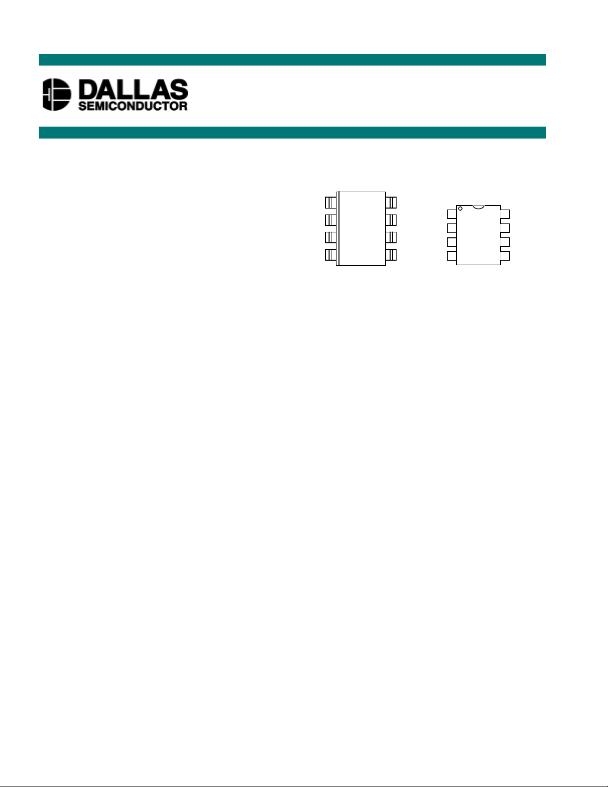
8-pin, 150-mil SOIC package and 8-pin µSOP
package
PIN ASSIGNMENT
SDA
SCL
T
OUT
GND
1 8
2 7
4
DS1721S
8-Pin SOIC (150-mil)
V
DD
SDA
A
0
SCL
A
1
T
OUT
A
2
GND
*
DS1721U
8-PIN µ-SOP
V
A
A
A
PIN DESCRIPTION
SDA - 2-Wire Serial Data Input/Output
SCL - 2-Wire Serial Clock
GND - Ground
T
A
A
A
V
OUT
0
1
2
DD
- Thermostat Output Signal
- Chip Address Input
- Chip Address Input
- Chip Address Input
- Power Supply Voltage (+5V)
DD
0
1
2
DESCRIPTION
The DS1721 2-Wire Digital Thermometer and Thermostat provides 12-bit temperature readings which
indicate the temperature of the device. Thermostatic settings and temperature readings are all
communicated to/from the DS1721 over a simple 2-wire serial interface. No additional components are
required; the device is truly a “temperature-to-digital” converter.
The DS1721 has three address bits that allow a user to multidrop up to eight sensors along the 2-wire bus,
greatly simplifying the bussing of distributed temperature sensing networks.
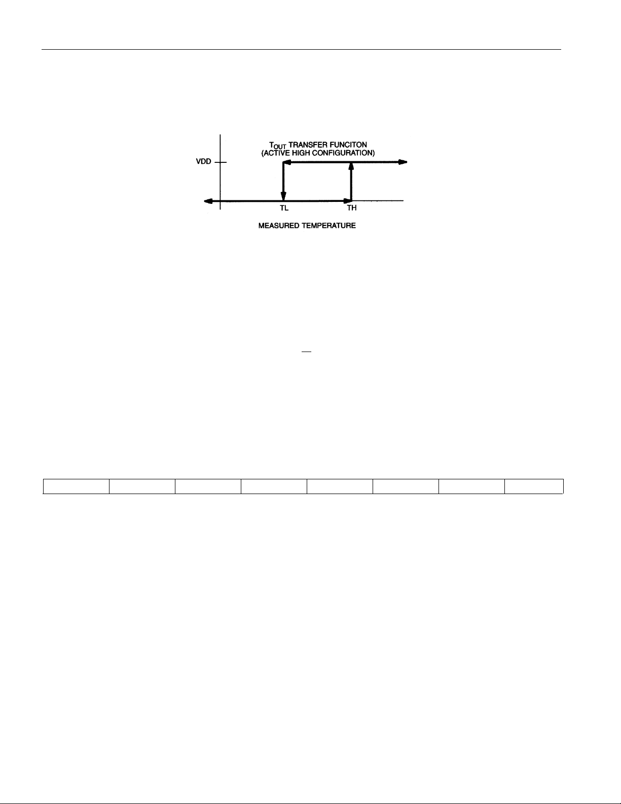
The thermal alarm output, T
temperature TH. The output remains active until the temperature is equal to or below the user-defined
temperature TL, allowing for any hysteresis necessary. The active state of T
user.
For applications that require faster conversion times, the user can adjust the readout resolution from 12 to
9 bits, effectively reducing the conversion time from 1.2 s (MAX) to 150 ms (MAX). This is particularl y
useful in applications where temperature changes large magnitudes very rapidly.
Applications for DS1721 include personal computers/services, cellular telephones, office equipment, or
any microprocessor-based, thermally sensitive system.
, is active when the temperature of the device exceeds a user-defined
OUT
is configurable by the
OUT
1 of 16 111999
Page 2
DETAILED PIN DESCRIPTION Table 1
PIN SYMBOL DESCRIPTION
1SDAData input/output pin. For 2-wire serial communication port.
2SCLClock input/output pin. For 2-wire serial communication port.
3T
OUT
Thermostat output. Active when temperature exceeds TH; will reset when
temperature falls below TL.
4 GND
5A2
6A1
7A0
Ground pin.
Address input pin.
Address input pin.
Address input pin.
8VDDSupply Voltage. 2.7V to 5.5V input power pin.
OVERVIEW
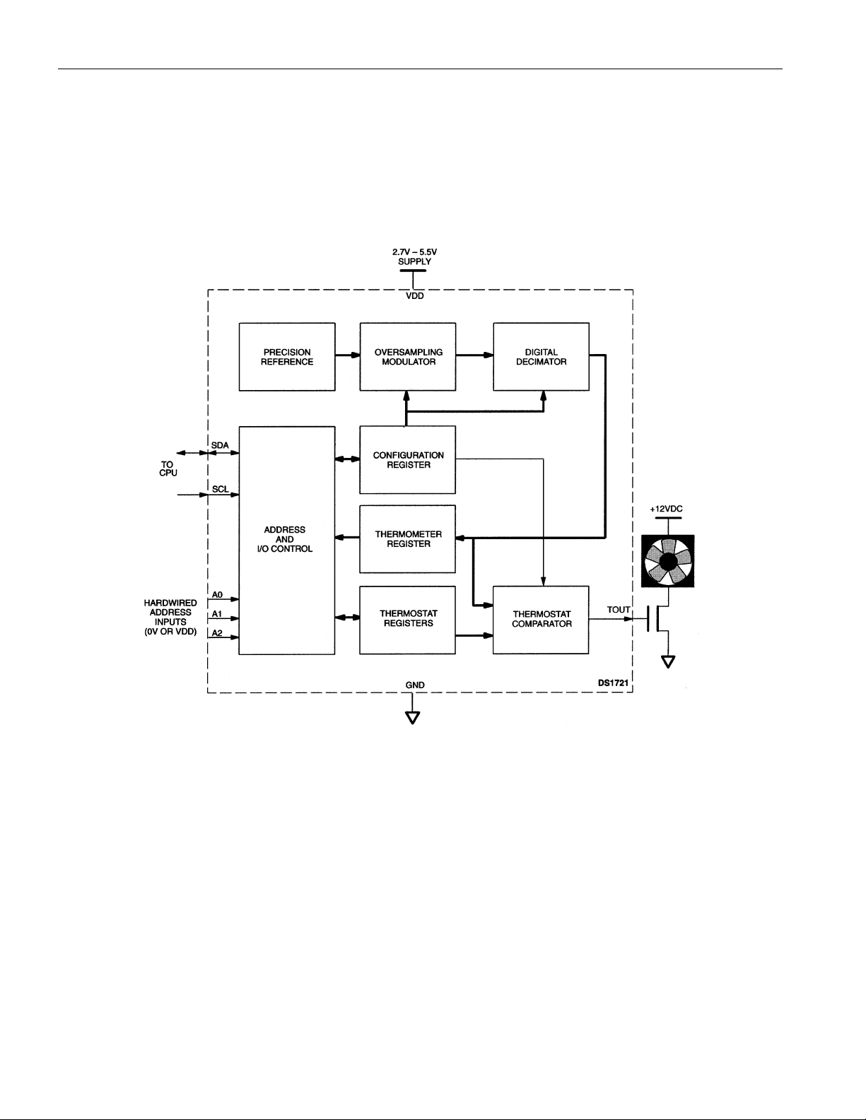
A block diagram of the DS1721 is shown in Figure 1.
The DS1721 consists of five major components:
1. Precision temperature sensor
2. Analog-to-digital converter
3. 2-wire interface electronics
DS1721
4. Data registers
5. Thermostat comparator
The factory-calibrated temperature sensor requires no external components. Upon power-up, the DS1721
is in an idle mode. Upon issuance of a Start Convert T command [51h], the DS1721 begins temperature
conversions with the default resolution of 12 bits (0.0625°C resolution). Following an 8-bit command
protocol, temperature data can be read over the 2-wir e interfa ce. The host can p eriodical l y read the valu e
in the temperature register, which contains the last completed conversion. As conversions are performed
in the background, reading the temperature register does not affect the conversion in progress.
In power-sensitive applications, the user can put the DS1721 in a “one-shot” mode, under which the
sensor will complete and store one temperature conversion and return to a low-power standby state. In
time-sensitive applications, the user can change the conversion resolution from 12 bits to 9, 10, or 11.
Each additional bit of resolution approximately doubles the conversion time, so 9-bit conversions can be
performed in less than a quarter of a second.
This is accomplished by issuing a command protocol t o the configuration register. It is recommend ed t hat
the user issue the command protocol to program the configuration register before any temperature
conversion commands are issued after power-up. This is due to the fact that the configuration data is
stored in volatile memory and will always power-up in the default state. The configuration register
defines the conversion mode, thermometer resolution/conversion time, and active stat e of the thermostat
comparator output. It also contains 3 status bits denoting the state of temperature conversions and
thermostat flags.
The user can also program over-temperature (TH) and under-temper ature (TL) setpoints for thermostatic
operation. The power-up state of TH is 80°C and that for TL is 75°C. The result of each temperature
conversion is compared with these setpoints. The thermostat output (T
) becomes active when the
OUT
measured temperature exceeds the programmed TH, and remains latched in the active state until
2 of 16
Page 3
DS1721
temperature falls below TL. Thus, any hysteresis can be realized for fan control without external
components.
Digital data is written to/read from the DS1721 via a 2-wire interface, and all communication is MSb
first. Multipoint sensing is possible with the DS1721 by uniquely setting the 3-bit address of up to eight
parts on the 2-wire bus.
DS1721 FUNCTIONAL BLOCK DIAGRAM Figure 1
3 of 16
Page 4
DS1721
OPERATION-Measuring Temperature
The core of DS1721 functionality is its direct-to-digital temperature sensor. The DS1721 measures
temperature through the use of an on-chip temperature measurement technique with an operation range
from -55°C to +125°C. The device can be configured to perform continuous conversions with the most
recent result being stored in the thermometer register. The device can also be configured to perform a
single conversion, store the result, and return to a standby mode. Regardless of the mode used, the digital
temperature is retrieved from the temperature register using the Read Temperature (AAh) command, as
described in detail in the “Command Set” section. The DS1721 power-up default has the s ensor set to
automatically perform 12-bit conversions continuously once the Start Convert T (51h) command is
issued. Details on how to change the settings after power-up are contained in the “OPERATIONProgramming” section.
The resolution of the temperature conversion can be configured as 9, 10, 11, or 12 bits, with 12-bit
readings as the default state. This equates to a temperature resolution of 0.5°C, 0.25°C, 0.125°C, or
0.0625°C. Following each conversion thermal data is stored in the thermometer register in two’s
complement format; the information can be retrieved over the 2-wire interface by issuing a Read
Temperature (AAh) command. Table 2 describes the exact relationship of output data to measured
temperature. The table assumes the DS1721 is configured for 12-bit resolution; if the device is configured
in a lower resolution mode, insignificant bits will contain zeros. The data is transmitted serially over the
2-wire serial interface, MSb first. The MSb of the temperature register contains the “sign” (S) bit,
denoting whether the temperature is positive or negative. For Fahrenheit usage, a lookup table or
conversion routine must be used.
TEMPERATURE/DATA RELATIONSHIPS Table 2
S262
5
MSb (UNIT = °C) LSb
-1
2
-2
2
-3
2
TEMP DIGITAL OUTPUT
+125°C 0111 1101 0000 0000 7D00h
+25.0625°C 0001 1001 0001 0000 1910h
+10.125°C 0000 1010 0010 0000 0A20h
+0.5°C 0000 0000 1000 0000 0080h
+0°C 0000 0000 0000 0000 0000h
-0.5°C 1111 1111 1000 0000 FF80h
-10.125°C 1111 0101 1110 0000 F5E0h
-25.0625°C 1110 0110 1111 0000 E6F0h
-55°C 1100 1001 0000 0000 C900h
4
2
-4
2
3
2
2
2
1
2
0
2
MSB
0000LSB
DIGITAL OUTPUT
(Binary)
(Hex)
OPERATION-Thermostat Control
In its operating mode, the DS1721 functions as a thermostat with programmable hysteresis, as sho wn in
Figure 2. The thermostat output updates as soon as a temperature conversion is complete. When the
DS1721’s temperature meets or exceeds the value stored in the high temperature trip register (TH), the
output becomes active, and will stay active until the temperature is equal to or below the temperature
stored in the low temperature trigger register (TL). In this way, any amount of hysteresis may be
obtained.
4 of 16
Page 5
DS1721
The active state for the totem-pole output is programmable by the user. The power-up default of the
DS1721 has TH=80°C, TL=75°C, and the output state active high. Refer to the “OPERATIONProgramming” section for instructions in adjusting the thermostat setpoints and T
active state.
COM
THERMOSTAT OUTPUT OPERATION Figure 2
OPERATION-Programming
There are two areas of interest in programming the DS1721: the Configuration/Status register and the
thermostat setpoints. All programming is done via the 2-wire interface using the protocols discussed in
the “Command Set” section.
Configuration/Status Register Programming
The configuration/status register is accessed via the Access Config (ACh) function command. Writing to
or reading from the register is determined by the R/W bit of the 2-wire cont rol byte (See “2-wire S erial
Data Bus” section). Data is read from or written to the configuration register MSb first. The format of the
register is illustrated below in Figure 3. The effect each bit has on DS1721 functionality is described
below along with the power-up state of the bit and its ability to be read or written to. The entire register is
volatile and will always power-up in the default state. Therefore, it is recommended that the user issue
any configuration programming commands immediately after power is cycled, before any other
commands are issued.
CONFIGURATION/STATUS REGISTER Figure 3
DONE X X U R1 R0 POL 1SHOT
MSb LSb
1SHOT = Temperature Conversion Mode. If 1SHOT is "1", the DS1721 will perform and store one
temperature conversion upon reception of the Start Convert T (51h) command. If 1SHOT is "0", the
DS1721 will continuously perform temperature conversions and store the last completed result in the
Thermometer Register. The user has read/write access to the bit and the power-up default state is "0"
(continuous mode).
POL = TCOM Polarity Bit. If POL is "1", the active state of the TCOM output will be high. A "0" stored
in this location sets the thermostat output to an active low state. The user has read/write access to the
POL bit, and the power-up default state is "1" (active high).
U = Undefined. This bit is used internally by the DS1721. It will be a "0" at power-up and will change to
a "1" once the Start Convert T [51h] command is issued. This is a “Don’t Care” on a write; i.e. The
DS1721 will ignore writes to this location.
5 of 16
Page 6

DS1721
R0, R1 = Thermometer Resolution Bits. Table 3 below defines the resolution of the digital thermometer,
based on the settings of these two bits. There is a direct tradeoff between resolution and conversion time,
as depicted in the DC Electrical Characteristics: Digital Thermometer table. The designer has read/write
access to R0 and R1, and the default state is R0="1" and R1="1" (12-bit conversions).
THERMOMETER RESOLUTION CONFIGURATION Table 3
MAX
THERMOMETER
R1 R0
RESOLUTION
0 0 9-BIT 0.15s
0 1 10-BIT 0.3s
1 0 11-BIT 0.6s
1 1 12-BIT 1.2s
X = Undefined. These bits are used internally by the DS1721.
DONE = Temperature Conversion Status Bit. "1" = conversion complete and "0" = conversion in
progress. The DONE bit is read-only, and the power-up state is "1". In the continuous conversion mode,
DONE = "0".
CONVERSION
TIME
Thermostat Setpoints Programming
The thermostat registers (TH and TL) define the setpoints for operation of the TCOM output. The
respective register can be accessed ov er the 2-wire bus via the Access TH (A1h) or Access TL (A2h)
commands. Reading from or writing to the respective register is controlled by the state of the R/W bit in
the 2-wire control byte (See “2-Wire Serial Data Bus” section).
The format of the TH and TL registers is a 12-bit 2’s complement representation of the temperature in °C.
The user can program the number of bits (9, 10, 11, or 12) fo r each TH and TL that cor respond to the
thermometer resolution configuration chosen. If the 9-bit mode is chosen, for example, the 3 least
significant bits of TH and TL will be ignored by the thermostat comparator. The format for both TH and
TL is shown in Figure 4. The power-up default of TH is 80°C and that for TL is 75°C.
TEMPERATURE/DATA RELATIONSHIPS Figure 4
S262
5
MSb (UNIT = °C) LSb
-1
2
-2
2
-3
2
TEMP DIGITAL OUTPUT
+80°C 0101 0000 0000 0000 5000h
+75°C 0100 1011 0000 0000 4B00h
+10.125°C 0000 1010 0010 0000 0A20h
+0.5°C 0000 0000 1000 0000 0080h
+0°C 0000 0000 0000 0000 0000h
-0.5°C 1111 1111 1000 0000 FF80h
-10.125°C 1111 0101 1110 0000 F5E0h
-25.0625°C 1110 0110 1111 0000 E6F0h
-55°C 1100 1001 0000 0000 C900h
4
2
-4
2
3
2
2
2
1
2
0
2
MSB
0000LSB
DIGITAL OUTPUT
(Binary)
(Hex)
6 of 16
Page 7

DS1721
If the user does not wish to take advantage of the thermostat capabilities of the DS1721, the 24 bits can be
used for general storage of system data that need not be maintained following a power loss. However, the
T
pin should be left floating if general data is stored in TH/TL.
OUT
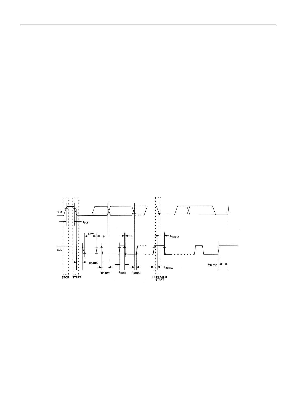
2-WIRE SERIAL DATA BUS
The DS1721 supports a bi-directional 2-wire bus and data transmission protocol. A device that sends data
onto the bus is defined as a transmitter, and a device receiving data as a receiver. The device that controls
the message is called a “master.” The devices that are cont roll ed by the master are “slaves.” The bus must
be controlled by a master device which generates the serial clock (SCL), controls the bus access, and
generates the START and STOP conditions. The DS1721 operates as a slave on the 2-wire bus.
Connections to the bus are made via the open-drain I/O lines SDA and SCL.
The following bus protocol has been defined (See Figure 5):
• Data transfer may be initiated only when the bus is not busy.
• During data transfer, the data line must remain stable whenever the clock line is HIGH. Changes in
the data line while the clock line is high will be interpreted as control signals.
Accordingly, the following bus conditions have been defined:
Bus not busy: Both data and clock lines remain HIGH.
Start data transfer: A change in the state of the data line, from HIGH to LOW, while the clock is HIGH,
defines a START condition.
Stop data transfer: A change in the state of the data line, from LOW to HIGH, while the clock line is
HIGH, defines the STOP condition.
Data valid: The state of the data line represents valid data when, after a START condition, the data line
is stable for the duration of the HIGH period of the clock signal. The data on the line must be changed
during the LOW period of the clock signal. There is one clock pulse per bit of data.
Each data transfer is initiated with a START condition and terminated with a STOP condition. The
number of data bytes transferred between START and STOP conditions is not limited, and is determined
by the master device. The information is transferred byte-wise and each receiver acknowled ges with a 9
bit.
Within the bus specifications a regular mode (100 kHz clock rate) and a fast mode (400 kHz clock rate)
are defined. The DS1721 works in both modes.
Acknowledge: Each receiving device, when addressed, is obliged to generate an acknowled ge after the
reception of each byte. The master device must generate an extra clock pulse which is associated with this
acknowledge bit.
th
A device that acknowledges must pull down the SDA line during the acknowledge clock pulse in such a
way that the SDA line is stable LOW during the HIGH period of the acknowledge related clock pulse. Of
course, setup and hold times must be taken into account. A master must signal an end of data to the slave
by not generating an acknowledge bit on the last byte that has been clocked out of the slave. In this case,
the slave must leave the data line HIGH to enable the master to generate the STOP condition.
7 of 16
Page 8

DS1721
DATA TRANSFER ON 2-WIRE SERIAL BUS Figure 5
Figure 6 details how data transfer is accomplished on the two-wire bus. Depending upon the state of the
R/W bit, two types of data transfer are possible:
Data transfer from a master trans mitter to a slave receiver. The 1
st
byte transmitted by the master is
the slave address. Next follows a number of data bytes. The slave returns an acknowledge bit after each
received byte.
Data transfer from a slave transmitter to a master receiver. The 1st byte (the slave address) is
transmitted by the master. The slave then returns an acknowledge bit. Next follows a number of data
bytes transmitted by the slave to the master. The master returns an acknowledge bit after all received
bytes other than the last byte. At the end of the last received byte, a ‘not acknowledge’ is returned.
The master device generates all of the serial clock pulses and the START and STOP conditions. A
transfer is ended with a STOP condition or with a repeated START condition. Since a repeated START
condition is also the beginning of the next serial transfer, the bus will not be released.
The DS1721 may operate in the following two modes:
Slave receiver mode: Serial data and clock are received through SDA and SCL. After each byte is
received, an acknowledge bit is transmitted. START and STOP conditions are recognized as the
beginning and end of a serial transfer. Address recognition is performed by hardware after r eception of
the slave address and direction bit.
Slave transmitter mode: The first b yte is received and handled as in the slave receiv er mode. However,
in this mode, the direction bit will indicate that the transfer direction is reversed. Serial data is transmitted
on SDA by the DS1721 while the serial clock is input on SCL. START and STOP conditions are
recognized as the beginning and end of a serial transfer.
8 of 16
Page 9

2-WIRE SERIAL COMMUNICATION WITH DS1721 Figure 6
DS1721
9 of 16
Page 10

DS1721
SLAVE ADDRESS
A control byte is the 1st byte received following the START condition from the master device. The
control byte consists of a 4-bit control code; for the DS1721, this is set as 1001 binary for r ead and write
operations. The next 3 bits of the control byte are the device select bits (A2, A1, A0). They are used b y
the master device to select which of eight devices are to be accessed. The s et bits are in effect the 3 l east
significant bits of the slave address. The last bit of the control byte (R/ W ) defines th e operation to be
performed. When set to a 1 a read operation is selected, and when s et to a 0 a writ e operati on is selected.
Following the START condition, the DS1721 monitors the SDA bus checking the device type identifier
being transmitted. Upon receiving the 1001 code and appropriate device select bits, the slave device
outputs an acknowledge signal on the SDA line.
COMMAND SET
Data and control information is read from and written to the DS1721 in the format shown in Figure 6. To
write to the DS1721, the master will issue the slave address of the DS1721 and the R/W bit will be set to
"0". After receiving an acknowledge, the bus master provides a command protocol. Aft er receiving this
protocol, the DS1721 will issue an acknowledge and the master may send data to the DS1721. If the
DS1721 is to be read, the master must send the command protocol as before then issue a repeated START
condition and the control byte again, this time with the R/ W bit set to "1" to allow reading of the data
from the DS1721. The command set for the DS1721 as shown in Table 4 is as follows:
Read Temperature [AAh]
This command reads the last temperature conversion result from the Thermometer Register in the format
described in the “OPERATION-Measuring Temperature” section. If one’s application can accept
thermometer resolution of only 1.0°C, the master only must read the first data b yte and follow with a
NACK and STOP. For higher resolution, both bytes must be read.
Access TH [A1h]
If R/ W is "0", this command writes to the TH register. After issuing this command, the next 2 bytes
written to the DS1721, in the format described for thermostat set-points, will set the high temperature
threshold for operation of the TOUT output. If R/W is "1", the value stored in this register is read back.
Access TL [A2h]
If R/ W is "0", this command writes to the TL register. After issuing this command, the next 2 bytes
written to the DS1721, in the format described for thermostat set-points, will set the high temperature
threshold for operation of the TOUT output. If R/
W is "1", the value stored in this register is read back.
Access Config [ACh]
If R/ W is "0", this command writes to the configuration register. After issuing this command, the next
data byte value is to be written into the configuration register. If R/W is "1", the next data byte read is the
value stored in the configuration register.
Start Convert T [51h]
This command begins a temperature conversion. No further data is required. In one-shot mode, the
temperature conversion will be performed and stored and then the DS1721 will remain idle. In continuous
mode, this command will initiate continuous conversions.
10 of 16
Page 11

DS1721
Stop Convert T [22h]
This command stops temperature conversion. No further data is required. This command may be used to
halt a DS1721 in continuous conversion mode. After issuing this command, the current temperature
measurement will be completed, stored and the DS1721 will remain idle until a Start Convert T is issued
to resume conversions.
DS1721 COMMAND SET Table 4
2-WIRE BUS DATA
INSTRUCTION DESCRIPTION PROTOCOL
REGISTER COMMANDS
Access
Configuration
Access TH
Access TL
Start Convert T
Stop Convert T
Read
Temperature
Writes to/Reads from 8-bit
configuration/status register
Writes to/Reads from
12-bit TH register
Writes to/Reads from
12-bit TL register
CONVERSION COMMANDS
Initiates temperature
conversion
Terminates continuous
conversions
Reads 12-bit
Temperature register
ACh 1 data byte 1
A1h 1 or 2 data bytes 1, 3
A2h 1 or 2 data bytes 1, 3
51h idle 2
22h idle 2
AAh Read 1 or 2 data bytes 3
AFTER ISSUING
PROTOCOL
NOTES
NOTES:
1. Data direction depends upon R/W bit in the 2-wire control byte.
2. In continuous conversion mode, a Stop Convert T command will halt continuous conversion. To
restart, the Start Convert T command must be issued. In one-shot mode, a Start Convert T command
must be issued for every temperature reading desired.
3. If the user only desires 8-bit thermometer readings, the master need only read 1 data byte and follow
with a NACK and STOP. If higher resolution is required, 2 bytes must be read.
11 of 16
Page 12

SAMPLE COMMAND SEQUENCE Table 5
Example: After power-up, initiates a temperature conversion, bus master reads temperature
BUS MASTER
MODE
TX RX START Bus Master initiates a START condition
TX RX <address, 0>
RX TX ACK DS1721 generates acknowledge bit
TX RX 51h Bus Master sends start convert T protocol
RX TX ACK DS1721 generates acknowledge bit
TX RX START Bus Master initiates a repeated START condition
TX RX <address, 0>
RX TX ACK DS1721 generates acknowledge bit
TX RX AAh Bus Master sends read temperature protocol
RX TX ACK DS1721 generates acknowledge bit
TX RX START Bus Master initiates a repeated START condition
TX RX <address, 1>
RX TX ACK DS1721 generates acknowledge bit
RX TX <1 data byte> DS1721 transmits MSB of temperature
TX RX ACK Bus Master generates acknowledge bit
RX TX <1 data byte> DS1721 transmits LSB of temperature
DS1721
MODE
DATA (MSB
FIRST)
COMMENTS
Bus Master sends DS1721 address; R/
Bus Master sends DS1721 address; R/
W = 0
W = 0
Bus Master sends DS1721 address; R/W =1
DS1721
12 of 16
Page 13
DS1721
SAMPLE COMMAND SEQUENCE Table 6
Example: Bus master programs the DS1721 for 11-bit conversions in the continuous mode with an active
low state for the thermostat output. It then programs TH=50°C and TL=45°C and starts temperature
conversions.
BUS MASTER
MODE
TX RX START Bus Master initiates a START condition
TX RX <address, 0>
RX TX ACK DS1721 generates acknowledge bit
TX RX ACh Bus Master sends access configuration protocol
RX TX ACK DS1721 generates acknowledge bit
TX RX 08h Bus Master programs configuration register as
RX TX ACK DS1721 generates acknowledge bit
TX RX START Bus Master Initiates a REPEATED START
TX RX <address, 0>
RX TX ACK DS1721 generates acknowledge bit
TX RX A1h Bus Master sends access TH protocol
RX TX ACK DS1721 generates acknowledge bit
TX RX 32h Bus Master writes MSB of TH (50°C)
RX TX ACK DS1721 generates acknowledge bit
TX RX 00h Bus Master writes LSB of TH (50°C)
RX TX ACK DS1721 generates acknowledge bit
DS1721
MODE
DATA (MSB
FIRST)
COMMENTS
Bus Master sends DS1721 address; R/
W = 0
described above. This will also clear thermostat
flags
condition
Bus Master sends DS1721 address; R/W = 0
TX RX START Bus Master initiates a REPEATED START
condition
TX RX <address, 0>
Bus Master sends DS1721 address; R/W = 0
RX TX ACK DS1721 generates acknowledge bit
TX RX A2h Bus Master sends access TL protocol
RX TX ACK DS1721 generates acknowledge bit
TX RX 2Dh Bus Master writes MSB of TL (45°C)
RX TX ACK DS1721 generates acknowledge bit
TX RX 00h Bus Master writes LSB of TL (45°C)
RX TX ACK DS1721 generates acknowledge bit
TX RX START Bus Master initiates a REPEATED START
condition
TX RX <address, 0>
Bus Master sends DS1721 address; R/W = 0
RX TX ACK DS1721 generates acknowledge bit
TX RX 51h Bus Master sends start convert protocol
RX TX ACK DS1721 generates acknowledge bit
TX RX STOP Bus Master initiates STOP condition
13 of 16
Page 14

DS1721
ABSOLUTE MAXIMUM RATINGS*
Voltage on VDD, Relative to Ground -0.3V to +7.0V
Voltage on any other pin, Related to Ground -0.3V to +7.0V
Operating Temperature -55°C to +125°C
Storage Temperature -55°C to +125°C
Soldering Temperature 260°C for 10 seconds
* This is a stress rating only and functional operation of the device at these or any other conditions
above those indicated in the operation sections of this specification is not implied. Exposure to
absolute maximum rating conditions for extended periods of time may affect reliability.
RECOMMENDED DC OPERATING CONDITIONS
(-55°C to +125°C; 2.7V ≤ V
PARAMETER SYMBOL CONDITION MIN TYP MAX UNITS NOTES
Supply Voltage V
DD
2.7 5.5 V 1
≤ 5.5V)
DD
DC ELECTRICAL CHARACTERISTICS (-55°C to +125°C; 2.7V ≤ VDD ≤ 5.5V)
PARAMETER SYMBOL CONDITION MIN TYP MAX UNITS NOTES
Input Logic High V
Input Logic Low V
SDA Output Logic
Low Voltage
T
Output Logic
OUT
Voltage
V
V
V
V
Input Current Each
I/O Pin
I/O Capacitance C
Standby Current I
Active Current I
IH
IL
OL1
OL2
OH
OL
I/O
DD1
DD
3 mA sink
current
6 mA sink
current
1 mA source
current
4 mA sink
current
0.4V ≤ V
≤ 0.9 V
I/O
DD
Active Temp.
Conversions
Communication
only
0.7
V
DD
-0.5
0 0.4 V 1
0 0.6 V 1
2.4 V 1
-10 +10 µA 2
V
DD
+0.5
0.3
V
DD
V1
V1
0.4 V 1
10 pF
1 µA 3, 4
1000 µA 3, 4
100 µA 3, 4
14 of 16
Page 15

DC ELECTRICAL CHARACTERISTICS:
DS1721
DIGITAL THERMOMETER (-55°C to +125°C; 2.7V ≤ V
≤ 5.5V)
DD
PARAMETER SYMBOL CONDITION MIN TYP MAX UNITS NOTES
DS1721
Thermometer Error
T
ERR
-10°C to +85°C ±1.0 °C 5
Resolution 9 12 bits
Conversion Time t
CONVT
9-bit
Conversions
10-bit
Conversions
11-bit
Conversions
12-bit
Conversions
125 150
250 300
ms
500 600
1000 1200
AC ELECTRICAL CHARACTERISTICS:
2-WIRE INTERFACE (-55°C to +125°C; V
PARAMETER SYMBOL CONDITION MIN TYP MAX UNITS NOTES
SCL Clock
Frequency
f
SCL
Bus Free Time
Between a STOP
and START
t
BUF
Condition
Hold Time
(Repeated) START
t
HD:STA
Condition
Low Period of
SCL Clock
High Period of
SCL Clock
t
LOW
t
HIGH
Setup Time for a
Repeated START
t
SU:STA
Condition
Data Hold Time t
Data Set-up Time t
HD:DAT
SU:DAT
Rise Time of both
SDA and SCL
Signals
Fall Time of both
SDA and SCL
Signals
Set-up time for
STOP Condition
Capacitive Load for
each Bus Line
t
SU:STO
C
Input Capacitance C
t
R
t
F
b
I
Fast Mode
Standard Mode
Fast Mode
Standard Mode
Fast Mode
Standard Mode
Fast Mode
Standard Mode
Fast Mode
Standard Mode
Fast Mode
Standard Mode
Fast Mode
Standard Mode
Fast Mode
Standard Mode
Fast Mode
Standard Mode
Fast Mode
Standard Mode
Fast Mode
Standard Mode
15 of 16
0
0
1.3
4.7
0.6
4.0
1.3
4.7
0.6
4.0
0.6
4.7
0
0
100
250
20+0.1
C
B
20+0.1
C
B
0.6
4.0
400
100
0.9 µs 7
300
1000
300
1000
400 pF 9
5pF
=2.7V to 5.5V)
DD
KHz
µs
µs 6
µs
µs
µs
ns 8
ns 8
ns 9
µs
Page 16
NOTES:
1. All voltages are referenced to ground.
2. I/O pins of fast mode devices must not obstruct the SDA and SCL lines if VDD is switched off.
DS1721
3. I
4. I
specified with T
DD
specified with VDD at 5.0V and SDA,SCL = 5.0V, 0°C to 70°C.
DD
pin open.
OUT
5. See typical accuracy curves for specification limits outside the temperature range indicated.
6. After this period, the first clock pulse is generated.
7. The maximum t
HD:DAT
has only to be met if the device does not stretch the LOW period (t
LOW
SCL signal.
8. A fast mode device can be used in a standard mode system, but the requirement t
>250 ns must
SU:DAT
then be met. This will automatically be the case if the device does not stretch the LOW period of the
SCL signal. If such a device does stretch the LOW period of the SCL signal, it must output the next
data bit to the SDA line tR MAX+t
1000+250 = 1250 ns before the SCL line is released.
SU:DAT
9. Cb - total capacitance of one bus line in pF.
TIMING DIAGRAMS Figure 7
) of the
TYPICAL DS1721 THERMOMETER PERFORMANCE CURVE Figure 8
TBD
16 of 16
 Loading...