

Page 1
DS1680
www.maxi
m-ic.com
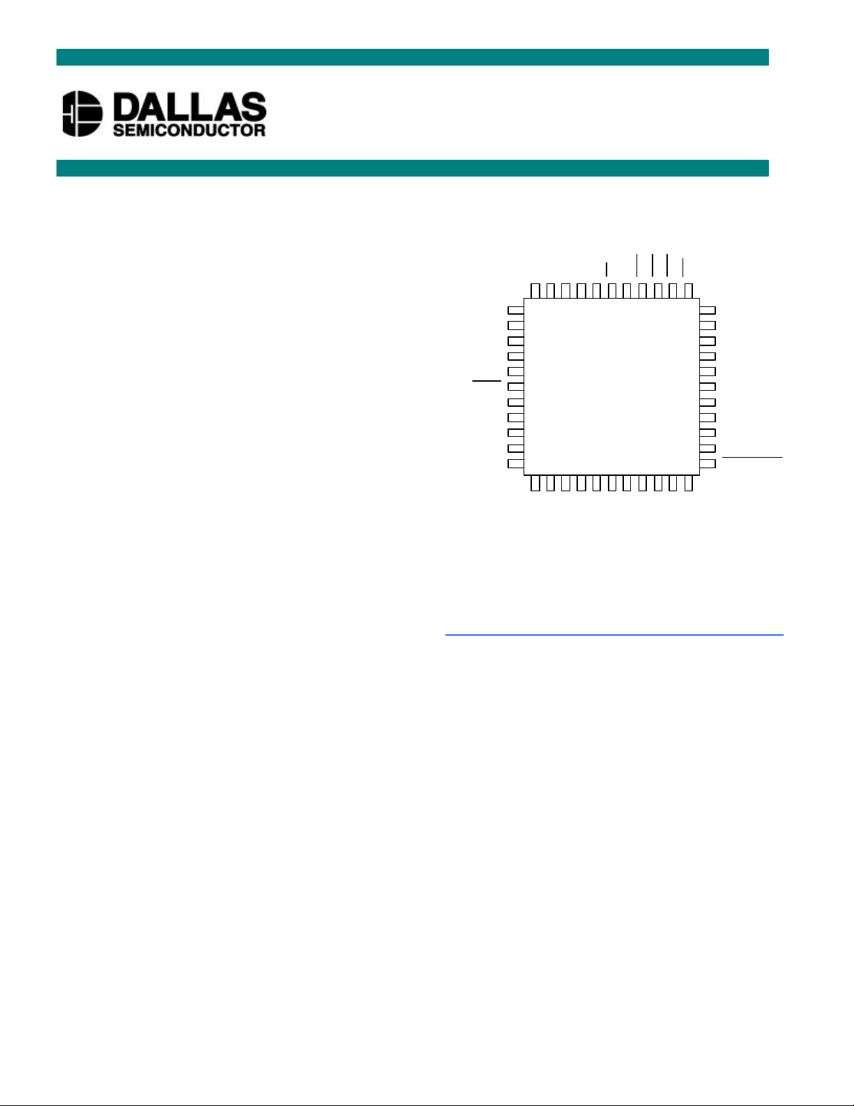
44-
Pin MQFP (10 x 10 x 2mm)
Package dimension information can be found at:
Portable System Controller
with Touch-Screen Control
FEATURES
PIN ASSIGNMENT
§ Real-time clock (RTC)
− Counts seconds, minutes, hours, date,
month, day of the week, and year with
leap-year compensation valid up to 2100
− Power control circuitry supports system
power-on from day/time alarm
§ Microprocessor monitor
− Halts microprocessor during power-fail
− Automatically restarts microprocessor
after power failure
− Monitors pushbutton for external
override
− Halts and resets an out of control
microprocessor
§ NV RAM control
− Automatic battery backup and write
protection to external SRAM
§ 1.25V threshold detector for power-fail
V
BAT
X1
X2
AVG
BHE
COEN
OUT_SELECT
CONVERT
PD_RESET
PEN_SELECT
ANSELIN
INT
44
1
12
AVS
I/O
REF
V
V
SCLK
AIN1
AIN0
CCO
CSSTVCCRST
Y-
X+
Y+
AVD
PFO
CEO
X-
PEN_OFF
CEI
34
33
2311
22
OSCIN
PFI
GND
D7
D6
D5
D4
D3
D2
D1
D0
NEW_DATA
warning
§ 10-bit analog-to-digital converter (ADC)
− Monotonic with no missing codes
http://www.maxim-ic.com/TechSupport/DallasPackInfo.htm
§ Four-wire analog resistive touch-screen
interface
ORDERING INFORMATION
DS1680FP-3 3.3V Operation
DS1680FP-5 5.0V Operation
DESCRIPTION
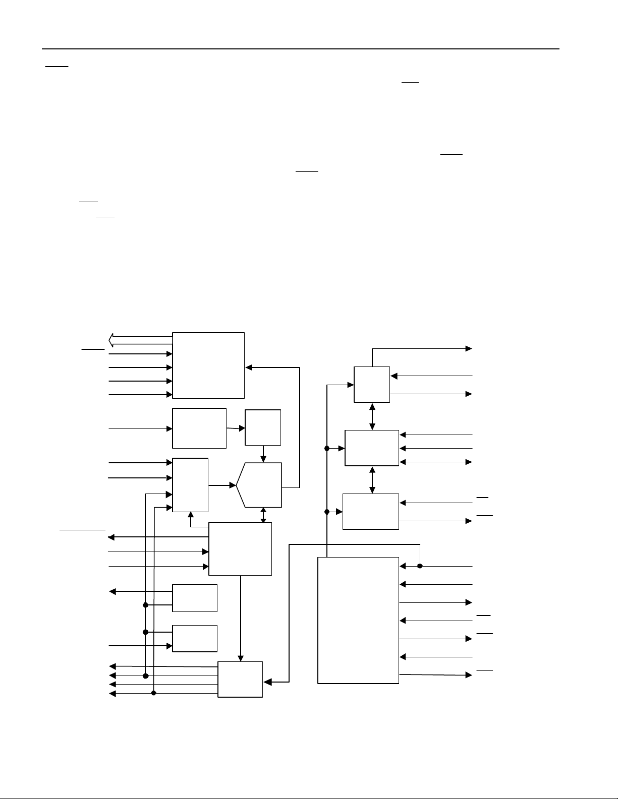
The DS1680 incorporates many functions necessary for low-power portable products, providing an RTC,
NV RAM controller, microprocessor monitor, power-f ail warning, 10-bit ADC, and a touch-screen
controller in one chip.
The RTC provides seconds, minutes, hours, day, date, month, and year information with leap-year
compensation as well as an alarm interrupt. This interrupt works when the DS1680 is powered by the
system power supply or when in battery-backup operation, so the alarm can be used to wake up a system
that is powered down.
1 of 23 110901
Page 2
DS1680
CLOCK
OSC
CLOCK
GEN
PANEL
DRIVE
CONVERT
CONTROL
10-BIT
ADC
INPUT
MUX
TOUCH
DETECT
POWER
CONTROL
RTC
SERIAL
INTERFACE
WATCHDOG
OUTPUT
MUX
BHE
OUT_SELECT
PEN_SELECT
AIN0
AIN1
COEN
CONVERT
PEN_OFF
PD_RST
D0-D7
OSCIN
X1X2INT
SCLK
CS
I/O
ST
RST
POWER SWITCH,
WRITE PROTECT,
NV CONTROL,
AND
POWER FAIL
WARNING
VCCV
V
CEI
CEO
PFI
PFO
ANSELIN
X+X-Y+Y-NEW_DATA
Automatic backup and write protection of an external SRAM is provided through the V
CCO
and
CEO pins. The backup energy source used to power the RTC is also used to retain RAM data in the
absence of VCC through the V
pin. The chip -enable output to SRAM, CE0 , is controlled during power
CCO
transients to prevent data corruption.
The DS1680’s microprocessor-monitor circuitry provides three basic functions. First, a precision
temperature-compensated reference and comparator circuit monitors the status of VCC. When an out -of-
tolerance condition occurs, an internal power-fail signal is generated that forces RST to the active state.
When VCC returns to an in-tolerance condition, the RST signal is kept in the active state for t
to allow
RPU
the power supply and processor to stabilize. The DS1680 debounces a pushbutton input and guarantees an
active RST pulse width of t
. The third function is a watchdog timer. The DS1680’s internal timer
RST
forces the RST signal to the active state if the strobe input is not driven low prior to watchdog time-out.
The DS1680 also provides a touch-screen controller along with a 10-bit successive approximation ADC.
The ADC is monotonic (no missing codes) and has an internal analog filter to reduce high frequency
noise.
DS1680 BLOCK DIAGRAM Figure 1
2 of 23
BAT
CCO
Page 3

DS1680
SIGNAL DESCRIPTIONS
VCC, GND (Digital Supply and Digital Ground) – DC power to the RTC, watchdog, X and Y drivers,
and power-switching circuitry is provided to the device on these pins.
V
(Backup Power Supply) – Battery input for standard 3V lithium cell or other energy source.
BAT
SCLK (Serial Clock Input) – SCLK is used to synchronize data movement on the serial interface.
I/O (Data Input/Output) – The I/O pin is the bidirectional data pin for the 3-wire interface.
CS (Chip Select) – The chip-select signal must be asserted high during a read or a write for
communication over the 3-wire serial interface.
V
(External SRAM Power Supply Output) – This pin is internally connected to V
CCO
within nominal limits. However, during power-fail V
Switchover occurs when V
drops below V
CC
CCSW
.
is internally connected to the V
CCO
INT (Interrupt Output) – The INT pin is an active-high output of the DS1680 that can be used as an
interrupt input to a microprocessor. The INT output remains high as long as the status bit causing the
interrupt is present and the corresponding interrupt-enable bit is set. The INT pin operates when the
DS1680 is powered by VCC or V
BAT
.
when VCC is
CC
BAT
pin.
CEI (SRAM Chip-Enable Input) – CEI must be driven low to enable the external SRAM.
CEO (SRAM Chip-Enable Output) – Chip-enable output for SRAM.
PFI (Power-Fail Input) – Power-fail comparator input. When PFI is less than 1.25V, PFO goes low;
otherwise PFO remains high. Connect PFI to GND or VCC when not used.
PFO (Power-Fail Output) – Power-fail output goes low and sinks current when PFI is less than 1.25V;
otherwise PFO remains high.
SI (Strobe Input) – The strobe input pin is used in conjunction with the watchdog timer. If the ST pin is
not driven low within the watchdog time period, the RST pin is driven low.
RST (Reset) – The RST pin functions as a microprocessor reset signal. This pin has an internal 47kΩ
pullup resistor.
X1, X2 – Connections for a standard 32.768kHz quartz crystal. For greatest accuracy, the DS1680 must
be used with a crystal that has a specified load capacitance of 6pF. There is no need for external
capacitors or resistors. Note: X1 and X2 are very high-impedance nodes. It is recommended that they and
the crystal be guard-ringed with ground and that high-frequency signals be kept away from the crystal
area. For more information about crystal selection and crystal layout considerations, please consult
Application Note 58, “Crystal Considerations with Dallas Real-Time Clocks.” The DS1680 will not
function without a crystal.
3 of 23
Page 4

DS1680
AVD, AVS (ADC Supply and Ground) – Power supply and ground for the ADC.
AIN0, AIN1 (Analog Inputs) – These pins are the analog inputs for the ADC.
V
(Voltage Reference) – Reference voltage for the ADC.
REF
X+, X- (Resistive Tablet X Plane Dri ver) – Connect to X-terminal of resistive tablet.
Y+, Y- (Resistive Tablet Y Plane Driver) – Connect to Y-terminal of resistive tablet.
CONVERT – Assert to logic 1 to request sample from AIN0 or AIN1. Use with ANSELIN input.
ANSELIN (Analog Select Input ) – Assert to logic 0 to select AIN0. Assert to logic 1 to select AIN1.
Use with CONVERT input.
BHE (Bus High Enable Input) – Drive to logic 1 to select high byte (data bits 2–9). Drive to logic 0 to
select low byte (data bits 0–1). The lower 6 bits will all be zeros when asserted low.
PEN_SELECT (Pen Select Input) – Assert to logic 1 to select X- or Y- data output. Assert to logic 0 to
select AIN0 or AIN1 data output. Use with OUT_SELECT input.
OUT_SELECT (Output Select Input) – Assert to logic 0 to select AIN0 or X- data. Assert to logic 1 to
select AIN1 or Y- data. Use with PEN_SELECT input.
COEN (Chip Output Enable) – The COEN pin must be asserted low to enable the ADC data to be
read on D0–D7.
D0-D7 (Data Bus) – Data output from ADC.
AVG (Data Average Select Pin) – Logic 1 selects data average mode; logic 0 selects raw data mode.
NEW_DATA (New Data Indicator) – A logic 0 pulse indicates that new data packet is available on
D0–D7.
OSCIN (Oscillator Input) – Input for the ADC clock.
PEN_OFF (Pen Detection Output) – Indicates pen not detected. Logic 1 if pen is not detected.
PD_RESET (Power Down/Reset Input) – Assert logic 1 for ≥10ns to reset. Hold at logic 1 for power-
down mode of the analog circuitry.
4 of 23
Page 5
DS1680
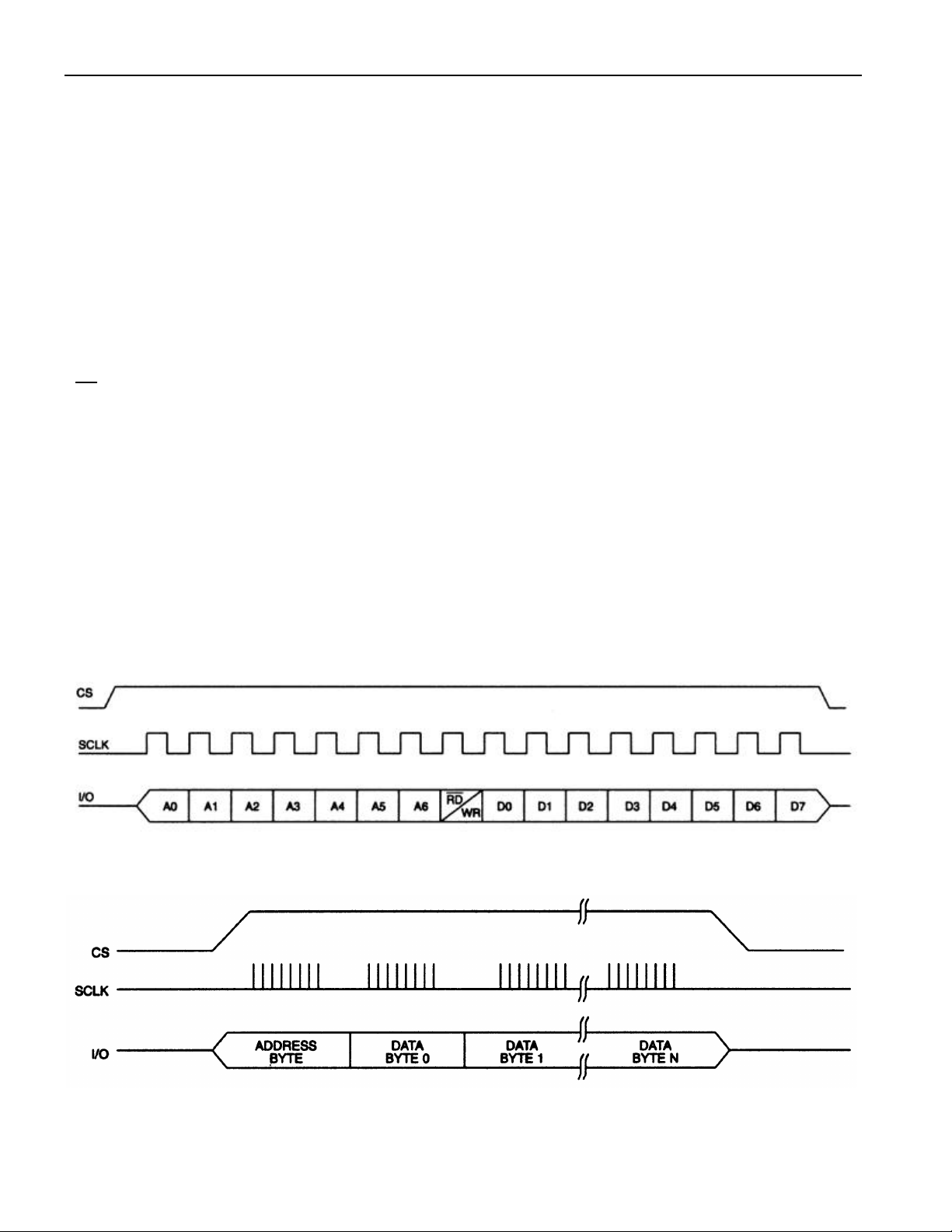
3-WIRE SERIAL INTERFACE
Communication with the RTC and watchdog is accomplished through a simple 3-wire interface
consisting of the chip select (CS), serial clock (SCLK), and input/output (I/O) pins.
All data transfers are initiated by driving the CS input high. The CS input serves two functions. First, CS
turns on the control logic, which allows access to the shift register for the address/command sequence.
Second, the CS signal provides a method of terminating either single byte or multip le byte (burst) data
transfer. A clock cycle is a sequence of a rising edge followed by a falling edge. For data input, data must
be valid during the clock’s rising edge and data bits are output on the clock’s falling edge. If the CS input
goes low, all da ta transfer terminates and the I/O pin goes to a high-impedance state.
Address and data bytes are always shifted LSB first into the I/O pin. Any transaction requires the
address/command byte to specify a read or write to a specific register followed by one or more bytes of
data. The address byte is always the first byte entered after CS is driven high. The most significant bit
(RD /WR) of this byte determines if a read or write will take place. If this bit is 0, one or more read cycles
will occur. If this bit is 1, one or more write cycles will occur.
Data transfers can occur one byte at a time or in multiple-byte burst mode. After CS is driven high an
address is written to the DS1680. After the address, one or more data bytes can be read or written. For a
single byte transfer one byte is read or written and then CS is driven low. Multiple bytes can be read or
written to the DS1680 after the address has been written. Each read or write cycle causes the register
address to automatically increment. Incrementing continues until the device is disabled. After accessing
register 0Dh, the address wraps to 00h.
Data transfer for single-byte transfer and multiple -byte burst transfer is illustrated in Figures 2 and 3.
SINGLE- BYTE DATA TRANSFER Figure 2
MULTIPLE-BYTE BURST TRANSFER Figure 3
5 of 23
Page 6
DS1680
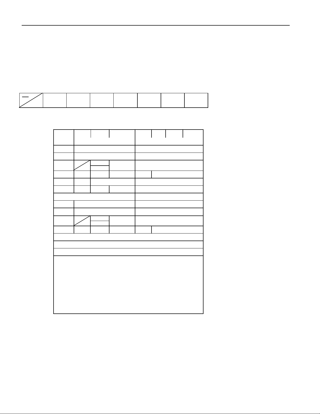
ADDRESS/COMMAND BYTE
Figure 4 shows the command byte for the DS1680. Each data transfer is initiated by a command byte.
Bits 0–6 specify the address of the registers to be accessed. The MSB (bit 7) is the read/write bit. This bit
specifies whether the accessed byte will be read or written. A read operation is selected if bit 7 is a zero
and a write operation is selected if bit 7 is a one. The address map for the DS1680 is shown in Figure 5.
ADDRESS/COMMAND BYTE Figure 4
7 6 5 4 3 2 1 0
RD
WR
A6 A5 A4 A3 A2 A1 A0
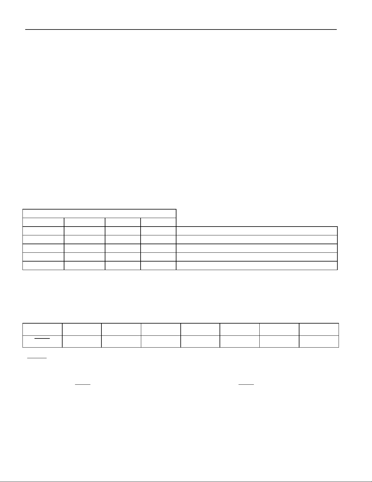
RTC/WATCHDOG ADDRESS MAP Figure 5
BIT7
00 0 10 SECONDS SECONDS
01 0 10 MINUTES MINUTES
02
0
12
24
10 HR
A/P
10 HR HOURS
03 0 0 0 0 0 DAY
04 0 0 10 DATE DATE
05 0 0 0 10 MO.
06 10 YEAR YEAR
07 M 10 SEC ALARM SECONDS ALARM
08 M 10 MIN ALARM MINUTES ALARM
09
M
12
24
10 HR
A/P
10 HR HOUR ALARM
0A M 0 0 0 0 DAY ALARM
0B CONTROL REGISTER
0C STATUS REGISTER
0D WATCHDOG REGISTER
0E
RESERVED
7F
BIT0
MONTH
6 of 23
Page 7
DS1680
CLOCK, CALENDAR, AND ALARM
The time and calendar information is accessed by reading/writing the appropriate register bytes. Note that
some bits are set to zero. These bits will always read zero regardless of how they are written. Also note
that registers 0Eh to 7Fh are reserved. These registers will always read zero regardless of how they are
written. The contents of the time, calendar, and alarm registers are in the binary-coded decimal (BCD)
format.
The DS1680 can run in either 12-hour or 24-hour mode. Bit 6 of the hours register is defined as the 12- or
24-hour mode select bit. When high, the 12-hour mode is selected. In the 12-hour mode, bit 5 is the
AM/PM bit with logic one being PM. In the 24-hour mode, bit 5 is the second 10-hour bit (20–23 hours).
The DS1680 also contains a time-of-day alarm. The alarm registers are located in registers 07h to 0Ah.
Bit 7 of each of the alarm registers are mask bits (Table 1). When all of the mask bits are logic 0, an
alarm will occur once per week when the values stored in time-keeping registers 00h to 03h match the
values stored in the time-of -day alarm registers. An alarm will be generated every day when mask bit of
the day alarm register is set to one. An alarm wil l be generated every hour when the day and hour alarm
mask bits are set to one. Similarly, an alarm will be generated every minute when the day, hour, and
minute alarm mask bits are set to one. When day, hour, minute, and second alarm mask bits are set to one,
an alarm will occur every second.
TIME- OF-DAY ALARM BITS Table 1
ALARM REGISTER MASK BITS (BIT 7)
Seconds Minutes Hours Day
1 1 1 1 Alarm once per second.
0 1 1 1 Alarm when seconds match.
0 0 1 1 Alarm when minutes and seconds match.
0 0 0 1 Alarm when hours, minutes and seconds match.
0 0 0 0 Alarm when day, hours, minutes and seconds match.
SPECIAL PURPOSE REGISTERS
The DS1680 has two additional registers (control register and status register) that control the RTC and
interrupts.
CONTROL REGISTER – 0Bh
BIT 7 BIT 6 BIT 5 BIT 4 BIT 3 BIT 2 BIT 1 BIT 0
EOSC
WP SP1 SP0 0 0 0 AIE
EOSC (Enable Oscillator) – This bit, when set to logic 0, will start the oscillator. When this bit is set to
a logic 1, the oscillator is stopped and the DS1680 is placed into a low-power standby mode (I
BAT
) when
in battery-backup mode. When the DS1680 is powered by VCC, the oscillator is always on regardless of
the status of the EOSC bit; however, the RTC is incremented only when EOSC is a logic 0.
SP0 and SP1 (Speed Select) – These bits select the on time of the X- and Y-measurement duty cycle.
The programmable duty cycle section has more detail.
WP (Write Protect) – Before any write operation to the RTC or any other registers, this bit must be logic
0. When high, the write-protect bit prevents a write operation to any register.
7 of 23
Page 8

DS1680
AIE (Alarm Interrupt Enable) – When set to a logic 1, this bit permits the interrupt request flag (IRQF)
bit in the status register to assert INT. When the AIE bit is set to logic 0, the IRQF bit does not initiate the
INT signal.
STATUS REGISTER – 0Ch
BIT 7 BIT 6 BIT 5 BIT 4 BIT 3 BIT 2 BIT 1 BIT 0
0 LOBAT 0 0 0 0 0 IRQF
LOBAT (Low Battery Flag) – This bit reflects the status of the backup power source connected to the
V
pin. When V
BAT
is greater than 2.5V, LOBAT is set to a logic 0. When V
BAT
is less than 2.3V,
BAT
LOBAT is set to a logic 1.
IRQF (Interrupt Request Flag) – A logic 1 in the interrupt request flag bit indicates that the current
time has matched the time of day alarm registers. If the AIE bit is also a logic 1, the INT pin will go high.
IRQF is cleared by reading or writing to any of the alarm registers.
POWER-UP/POWER-DOWN CONSIDERATIONS
When VCC is applied to the DS1680 and reaches a level greater than V
becomes fully accessible after t
VCC drops below V
, the device is switched over to the V
CCSW
(250ms typical). Before t
RPU
elapses, some inputs are disabled. When
RPU
supply.
BAT
During power-up, when VCC returns to an in-tolerance condition, the RST pin is kept in the active state
for 250ms (typical) to allow the power supply and microprocessor to stabilize.
(trip point), the device
CCTP
NONVOLATILE SRAM CONTROL LER
The DS1680 provides automatic backup and write protection for an external SRAM. This function is
provided by gating the chip-enable signal and by providing a constant power supply through the V
CCO
pin.
The DS1680 nonvolatizes the external SRAM by write-protecting the SRAM and by providing a backup
power supply in the absence of VCC. When V
falls below V
CC
, access to the external SRAM is
CCTP
prohibited by forcing CE0 high regardless of the level of CEI . Upon power-up, access is prohibited until
the end of t
RPU
.
POWER-FAIL COMPARATOR
The PFI input is connected to an internal reference. If PFI is less than 1.25V, PFO goes low. The powerfail comparator can be used as an undervoltage detector to signal an impending power supply failure.
PFO can be used as a µP interrupt input to prepare for power-down. For battery conservation, the
comparator is turned off and PFO is held low when in battery-backup mode.
ADDING HYSTERESIS TO THE POWER -FAIL COMPARATOR
Hysteresis adds a noise margin to the power-fail comparator and prevents PFO from oscillating when
VIN is near the power-fail comparator trip point. Figure 6 shows how to add hysteresis to the power-fail
comparator. Select the ratio of R1 and R2 such that PFI sees 1.25V when VIN falls to the desired trip
point (VTRIP). Resistors R2 and R3 adds hysteresis. R3 will typically be an order of magnitude greater
than R1 or R2. R3 should be chosen so it does not load down the PFO pin. Capacitor C1 adds noise
filtering and has a value of typically 1.0µF (See Figure 6 for a schematic diagram and equations.)
8 of 23
Page 9

DS1680
POWER-FAIL COMPARATOR Figure 6
+5V
V
CC
R1
VIN
PFI
V
TRIP
C1
= 1.25
R2 R3
R1 + R2
R2
VI – 1.25
R1
+
to µP
V
= 1.25 /
H
5 - 1.25
R3
DS1680
PFO
GND
R2||R3
R1 + R2||R3
1.25
=
R2
9 of 23
Page 10

DS1680
MICROPROCESSOR MONITOR
The DS1680 monitors three vital conditions for a microprocessor: power supply, software execution, and
external override.
First, a precision temperature-compensated reference and comparator circuit monitors the status of VCC.
When an out-of -tolerance condition occurs, an internal power-fail signal is generated that forces the RST
pin to the active state, thus warning a processor-based system of impending power failure. When VCC
returns to an in-tolerance condition upon power-up, the reset signal is kept in the active state for t
RST
to
allow the power supply and microprocessor to stabilize. Note, however, that if the EOSC bit is set to a
logic 1 (to disable the oscillator during battery-backup mode), the RST signal will be kept in an active
state for t
plus the start-up time of the oscillator.
RST
The second monitoring function is pushbutton reset control. The DS1680 provides for a pushbutton
switch to be connected to the RST output pin. When the DS1680 is not in a reset cycle, it continuously
monitors the RST signal for a low-going edge. If an edge is detected, the DS1680 will debounce the
switch by pulling the RST line low. After the internal timer has expired, the DS1680 will continue to
monitor the RST line. If the line is still low, the DS1680 will continue to monitor the line looking for a
rising edge. Upon detecting release, the DS1680 will force the RST line low and hold it low for t
RST
.
The third microprocessor monitoring function provided by the DS1680 is a watchdog timer. The
watchdog timer function forces RST to the active state when the ST input is not stimulated within the
predetermined time period. The time period is set by the time delay (TD) bits in the watchdog register.
The time delay can be set to 250ms, 500ms, or 1000ms. If TD0 and TD1 are both set to zero, the
watchdog timer is disabled. When enabled, the watchdog timer starts timing out from the set time period
as soon as RST is inactive. The default setting is for the watchdog timer to be enabled with 1000ms time
delay. If a high-to-low transition occurs on the ST input pin prior to time-out, the watchdog timer is reset
and begins to time-out again. If the watchdog timer is allowed to time-out, the RST signal is driven to the
active state for t
. The ST input can be derived from microprocessor address signals, data signals,
RST
and/or control signals. To guarantee that the watchdog timer does not time-out, a high-to-low transition
must occur at or less than the minimum period.
WATCHDOG REGISTER – 0Dh
BIT 7 BIT 6 BIT 5 BIT 4 BIT 3 BIT 2 BIT 1 BIT 0
0 0 0 0 0 0 TD1 TD0
WATCHDOG TIME-OUT BITS Table 2
TD1 TD0 WATCHDOG TIME-OUT
0 0 Watchdog Disabled
0 1 250ms
1 0 500ms
1 1 1000ms
10 of 23
Page 11

DS1680
RESISTIVE TOUCH SCREEN (4-WIRE)
Resistive touch screens consist of two resistive plates that are separated by a small gap. Each plate has an
electrode at each end; when the screen is touched the pressure forces the two plates to come in contact at
the exact position of the touch. To get the x-coordinate position, the DS1680 will drive the X-plane
resistive film (via X+ and X-) and sense the voltage picked up by the Y-plane resistive film (via Y+ and
Y-). Next, to get the y-coordinate position, the DS1680 will drive the Y- plane resistive film and sense the
voltage picked up by the X-plane resistive film.
ANALOG-TO-DIGITAL CONVERTER (ADC)
The DS1680 provides a 10-bit ADC. Two multiplexed analog inputs are provided through the AIN0 and
AIN1 pins along with two other inputs on the X- and Y- pins. The ADC is monotonic (no missing codes)
and uses a successive approximation tec hnique to convert the analog signal into a digital code.
An analog-to-digital conversion is the process of assigning a digital code to an analog input voltage. This
code represents the input value as a fraction of the full-scale voltage (FSV) range. The FSV range is then
divided by the ADC into 1024 codes (10 bits), and is bound by an upper limit equal to the reference
voltage and the lower limit, which is ground.
On-chip circuitry detects if the pen is in contact with the digitizer tablet. The pen-detection status is
indicated on pin (PEN_OFF) and can be used by the system for signaling end -of-stroke for handwriting
recognition software purposes. If no pen is detected, PEN_OFF will be pulled to logic 1 and no
coordinate data will be made available. PEN_OFF at logic 0 indicates that a pen is detected on the
digitizer tablet and its coordinate position will be made available on D0–D7. The NEW_DATA pin
pulses low to indicate when a new coordinate data pair is available.
When the AVG pin is set to logic 0, the data at pins D0 –D7 will indicate the most recent sample of the
ADC. Setting the AVG pin to logic 1 invokes the data averaging mode. In this mode, the data output on
D0–D7 will indicate the rolling average of the four most recent samples of the ADC.
The DS1680 continuously monitors the CONVERT and ANSELIN signals; on the internal clock’s rising
edge (state cycle), the corresponding AIN0 or AIN1 conversion is requested. The conversion request
must be completed before T0 (Figure 7c) in order for AIN0 and/or AIN1 to be sampled and converted in
the present conversion cycle; otherwise AIN0 and/or AIN1 will be sampled and converted in the next
conversion cycle. The logic level of the ANSELIN input will determine whether a sample is taken from
the AIN0 or AIN1 input. Table 3 lists the specific analog input that is selected by this signal. Figure 8
shows the required timing associated with CONVERT and ANSELIN. If the state of ANSELIN changes
while CONVERT is at logic 1 and you meet the timing requirements of figure 8, both AIN0 and AIN1
conversions are requested. If the ANSELIN does not change states while CONVERT is at
logic 1, only AIN0 or AIN1 conversion is requested. If a pen is detected during a conversion request, then
X and Y will be sampled and converted pr ior to the AIN0 and/or AIN1 conversion. The AIN0 and AIN1
conversion result is output on the D0 –D7 as defined in the Parallel Interface section.
ANALOG INPUT SELECTION Table 3
ANSELIN ANALOG INPUT
0 AINO
1 AIN1
11 of 23
Page 12

DS1680
PROGRAMMABLE DUTY CYCLE
The current required to take an X or Y measurement is V
V
= 5V, the current required is 20mA. The average current is the current during the measurement,
AVD
multiplied by the ratio of the time the drivers are on, to the power of total sample time. In order to
minimize the average current, the on-time should be limited to the minimum time required for the tablet
RC delay.
Experimental data suggests that a typical RC time constant is between 4µs and 5µs for a resistive touch
screen. In order to achieve 10-bit resolution, the settling time must be eight time constants. This creates a
requirement of a minimum of 80 µs on-time total, 40µs for each X and Y measurement.
To provide both low power and high sample rate, the on-time for the X- and Y-measurement duty cycle is
programmable. Bits 4 and 5 (SP0 and SP1) of the control register (0Bh) select the on-time of four
different frequency ranges. The frequencies given are the maximum frequency for that timing range,
which will not violate the 40µs-per-measurement requirement.
SP1 SP0 FREQUENCY RANGE (MHz)
AVERAGE
CURRENT (A)
0* 0* 2.0 870µ 543 5
0 1 2.8 1.217m 760 7
1 0 4.0 1.739m 1086 10
1 1 5.0 2.261m 1359 13
*This is the default setting
Average current is the current required for the measurement, averaged out over the entire sample. This
average current is only related to the measurement phase when the drivers are on. The average current
will be drawn from the VCC supply. There is also current associated with the pen-detection phase, the
ADC, and the control logic.
The number of cycles indicated is the number of on-time state cycles. One state cycle is 16 main clock
cycles. If the frequency range is 2.0MHz, the state frequency is 2MHz/16 = 125kHz. There are 230 state
cycles in one complete sample. The number of cycles can be used to calculate the settling time and the
sample rate.
Example 1:
Frequency Range : 2.0MHz
Input Clock Frequency : 1.8432MHz
tsettle = (1 / 1.8432e6) x 16 x 5 = 43.4µs
Iavg = (10 / 230) x 20mA = 870µA
Sample Rate = 1.8432e6 / (16 x 230) = 501 samples/sec
Example 2:
Frequency Range : 2.8MHz
Input Clock Frequency : 1.8432MHz
tsettle = (1 / 1.8432e6) x 16 x 7 = 60.8µs
Iavg = (14 / 230) / x 20mA = 1.217mA
Sample Rate = 1.8432e6 / (16 x 230) = 501 samples/sec
/ RD. In the case of RD = 250O and
AVD
SAMPLES/SEC NO. OF
CYCLES
12 of 23
Page 13

DS1680
CONVERSION TIMING Figure 7a
Pen Down
PEN_OFF
X - Y
Measure
PD A0 A1X Y
A0 - A1
Measure
PD PDPDPDPD X XXX Y Y YY A0A0 A1A1
A1A0PDPD PDPD
NEW_DATA
AVG = 0 (Disabled)
NEW_DATA
AVG = 1 (Enabled)
X to Y MEASUREMENT Figure 7b
115 state cycles
30 28-3610-18 13-5 21
1001 00
PD
11
X-drivers
on
13-5
111001 00
Y-drivers
on
30
PD
1 State Cycle = 16 Main Clock Cycles
AIN0 to AIN1 MEASUREMENT Figure 7c
115 state cycles
30 20618 6 35 30
PD A0
PDA1
1 State Cycle = 16 Main Clock Cycles
T
0
13 of 23
Page 14

DS1680
CONVERT AND ANSELIN TIMING Figure 8
must be at least
2 state cycles
CONVERT
AIN0 conversion requested
ANSELIN = 0
must be at least 4 state cycles
CONVERT
both AIN0 and AIN1 conversion requested
ANSELIN
CONVERT
ANSELIN = 1
must be at least
2 state cycles
must be at least
2 state cycles
must be at least
2 state cycles
AIN1 conversion requested
14 of 23
Page 15

DS1680
PARALLEL INTERFACE
The ADC output is available on the data bus at pins D0–D7. A logic 0 on COEN will enable data onto the
data bus so that the DS1680 can be used in parallel with other devices. PEN_SELECT and
OUT_SELECT are used to decode which analog output (X-, Y-, AIN0, or AIN1) is outp ut on the data bus
when COEN is asserted low. Since the device offers 10-bit resolution, the BHE pin is used to decode the
10 bits of data on the data bus. A logic 1 on BHE will enable data bits B2 –B9. A logic 0 will enable data
bits B0–B1 along with the six LSBs = 0. The status pin ( NEW_DATA ) pulses low to indicate that new
coordinate or conversion is available. The output can be read while NEW_DATA is low or after it has
gone high. Output selection and parallel data format is shown below.
OUTPUT SELECTION Table 4
PEN_SELECT OUT_SELECT ANALOG OUTPUT
0 0 AIN0
0 1 AIN1
1 0 X1 1 Y-
PARALLEL DATA FORMAT
MSB LSB
High Byte BHE = 1 B9 B8 B7 B6 B5 B4 B3 B2
Low Byte BHE = 0 B1 B0 0 0 0 0 0 0
POWER MANAGEMENT (ADC AND PEN-INPUT PROCESSOR)
The DS1680 analog circuitry can be placed into a low-power mode by asserting and holding the
PD_RESET pin at logic 1. Normal operation will resume when PD_RESET is returned to logic 0.
To further conserve power, the pen-detection circuitry will automatically switch the analog circuitry to
power-down mode whenever there is no pen input detected for more than three seconds. Normal
operation will automatically resume when any one of the following three events occur: pen down is
detected, the CONVERT signal is activated, or chip is reset (PD_RESET pulled to logic 1 and then
returned to logic 0).
15 of 23
Page 16

DS1680
ABSOLUTE MAXIMUM RATINGS*
Voltage Range on Any Pin Relative to Ground -0.3V to +7.0V
Operating Temperature Range 0°C to +70°C
Storage Temperature Range -55°C to +125°C
Soldering Temperature Range See J-STD-020A Specification
*This is a stress rating only and functional operation of the device at these or any other conditions beyond
those indicated in the operation sections of this specification is not implied. Exposure to absolute
maximum rating conditions for extended periods of time can affect reliability.
RECOMMENDED DC OPERATING CONDITIONS (0°C to +70°C)
PARAMETER SYMBOL MIN TYP MAX UNITS NOTES
Digital Power Supply Voltage
3.3V Operation
Digital Power Supply Voltage
5V Operation
Input Logic 1 VIH 2.0
V
CC, VAVD,
V
REF
V
CC, VAVD,
V
REF
2.97 3.3 3.63 V
4.5 5.0 5.5 V
VCC + 0.3
V
Input Logic 0 VIL -0.3 +0.8 V
Battery Voltage V
2.5 3.7 V
BAT
DC ELECTRICAL CHARACTERISTICS (0°C to +70°C; VCC = 5.0V ± 10%)
PARAMETER SYMBOL MIN TYP MAX UNITS NOTES
Input Leakage ILI -1 +1
CS Leakage ILO 260
Logic 1 Output (I
Logic 0 Output (I
Active Supply Current (No Pen Detect) I
Active Supply Current (Pen Detected) I
Standby Current I
Oscillator Current I
Battery Current (Oscillator Off) I
= -0.4mA) VOH 2.4 V 1
OUT
= 1.5mA) VOL 0.4 V 2
OUT
200 500 µA 3
CCA
5 mA 19
CCPD
175 300
CCS
300 500 nA 17
OSC
100 nA 18
BAT
Internal RST Pullup Resistor RP 25 47 87
VCC Trip Point V
VCC Switchover V
4.15 4.33 4.50 V
CCTP
2.67 2.78 V 12, 20
CCSW
µA
µA
µA
kΩ
Pushbutton Detect PBDV 0.8 2.0 V
Pushbutton Release PBRD 0.3 0.8 V
Output Voltage V
V
Output Current (Source = VCC) I
CCO
V
Output Current (Source = V
CCO
BAT)
I
PFI Input Threshold V
PFI Input Leakage I
PFO Output Voltage, I
= -0.4mA
OH
VOH
CCO
CCO1
CCO2
PFI
PFI
VCC - 0.3
V 11
150 mA 13
150
µA
1.15 1.25 1.35 V
-25 25 nA
VCC - 1.5
V
7
4
14
PFO Output Voltage, I
= 1.5mA
OL
VOL 0.4 V
16 of 23
Page 17

DS1680
DC ELECTRICAL CHARACTERISTICS (0°C to +70°C; VCC = 3.3V ± 10%)
PARAMETER SYMBOL MIN TYP MAX UNITS NOTES
Input Leakage ILI -1 +1
CS Leakage ILO 170
Logic 1 Output (I
Logic 0 Output (I
Active Supply Current (No Pen Detect) I
Active Supply Current (Pen Detected) I
Standby Current I
Oscillator Current I
Battery Current (Oscillator Off) I
= -0.4mA) VOH 2.4 V 1
OUT
= 1.5mA) VOL 0.4 V 2
OUT
115 300 µA 3
CCA
3 mA 19
CCPD
110 200
CCS
300 500 nA 17
OSC
100 nA 18
BAT
Internal RST Pullup Resistor RP 25 47 87
VCC Trip Point V
VCC Switchover V
2.75 2.86 2.97 V
CCTP
2.67 2.78 V 12, 20
CCSW
µA
µA
µA
kΩ
7
4
Pushbutton Detect PBDV 0.8 2.0 V
Pushbutton Release PBRD 0.3 0.8 V
Output Voltage V
V
Output Current (Source = VCC) I
CCO
V
Output Current (Source = V
CCO
BAT)
I
PFI Input Threshold V
PFI Input Leakage I
PFO Output Voltage, I
PFO Output Voltage, I
= -0.4mA
OH
=1.5mA
OL
VCC-0.3
CCO
80 mA 13
CCO1
100
CCO2
1.15 1.25 1.35 V
PFI
-25 25 nA
PFI
VOH VCC-1.5
V 11
µA
V
VOL 0.4 V
14
CAPACITANCE (TA = +25°C)
PARAMETER SYMBOL MIN TYP MAX UNITS NOTES
Input Capacitance CI 10 pF
I/O Capacitance C
15 pF
I/O
Crystal Capacitance CX 6 pF
3-WIRE INTERFACE CHARACTERISTICS (0°C to +70 °C; VCC = 5.0V ± 10%)
PARAMETER SYMBOL MIN TYP MAX UNITS NOTES
Data to Clock Setup tDC 50 ns 8
CLK to Data Hold t
CLK to Data Delay t
70 ns 8
CDH
200 ns 8, 9, 10
CDD
CLK to Low Time tCL 250 ns 8
CLK to High Time tCH 250 ns 8
CLK Frequency t
2.0 MHz 8
CLK
CLK Rise and Fall tR, tF 500 ns
CS to CLK Setup tCC 1
CLK to CS Hold t
CS Inactive Time t
CS to I/O High-Z t
250 ns 8
CCH
1
CWH
70 ns 8
CDZ
µs
µs
8
8
17 of 23
Page 18

DS1680
3-WIRE INTERFACE CHARACTERISTICS (0°C to +70 °C; VCC = 3.3V ± 10%)
PARAMETER SYMBOL MIN TYP MAX UNITS NOTES
Data to Clock Setup tDC 150 ns 8
CLK to Data Hold t
CLK to Data Delay t
CLK to Low Time tCL 750 ns 8
CLK to High Time tCH 750 ns 8
CLK Frequency t
CLK Rise and Fall tR, tF 1500 ns
CS to CLK Setup tCC 3
CLK to CS Hold t
CS Inactive Time t
CS to I/O High-Z t
ADC CHARACTERISTICS (0°C to +70°C; VCC, V
PARAMETER SYMBOL MIN TYP MAX UNITS NOTES
Resistance of Digitizer Film RD 250 600 1000 Ω
210 ns 8
CDH
600 ns 8, 9, 10
CDD
0.667 MHz 8
CLK
µs
750 ns 8
CCH
3
CWH
210 ns 8
CDZ
AVD
µs
= 5.0V ± 10%)
8
8
Resistance of On-Chip Driver R
Parasitic Capacitance Between X-
and Y-Plates of Digitizer
Ladder Resistance R
ADC Active Current I
ADC Standby Current I
Reference Current I
12 25 Ω
DRIVER
CXY 5 10 nF
8 25 60 kΩ
REF
450 650 µA 5
AVDA
120 200 µA 6
AVDS
200 650 µA
REF
Input Leakage (AIN0, AIN1) ILI 10 nA
Analog Input Capacitance CIN 10 15 pF
Resolution 10 Bits
Differential Nonlinearity EDL ±0.5 ±1.0 LSB
Integral Nonlinearity EIL ±0.5 ±1.0 LSB
Offset Error EOS ±1.0 ±1.5 LSB
Gain Error EG ±0.25 ±1.0 %
ADC Clock Frequency F
Multiplexer Selector Path
Propagation Delay
5.0 MHz
OSCIN
t
60 ns
MUX
COEN Falling Edge to Data Bus
Driven
COEN Rising Edge to Data Bus
High-Z
18 of 23
t
40 ns
OEA
t
40 ns
OEZ
Page 19

DS1680
ADC CHARACTERISTICS (0°C to +70°C; VCC, V
= 3.3V ± 10%)
AVD
PARAMETER SYMBOL MIN TYP MAX UNITS NOTES
Resistance of Digitizer Film RD 250 600 1000 Ω
Resistance of On-Chip Driver R
Parasitic Capacitance Between Xand Y-Plates of Digitizer
Ladder Resistance R
ADC Active Current I
ADC Standby Current I
Reference Current I
15 30 Ω
DRIVER
CXY 5 10 nF
8 25 60 kΩ
REF
320 450 µA 5
AVDA
50 150 µA 6
AVDS
150 550 µA
REF
Input Leakage (AIN0, AIN1) ILI 10 nA
Analog Input Capacitance CIN 10 15 pF
Resolution 10 Bits
Differential Nonlinearity EDL ±0.5 ±1.0 LSB
Integral Nonlinearity EIL ±0.5 ±1.0 LSB
Offset Error EOS ±1.0 ±1.5 LSB
Gain Error EG ±0.25 ±1.0 %
ADC Clock Frequency F
Multiplexer Selector Path
Propagation Delay
COEN Falling Edge to Data Bus
Driven
COEN Rising Edge to Data Bus
High-Z
2.5 MHz
OSCIN
t
120 ns
MUX
t
80 ns
OEA
t
80 ns
OEZ
POWER-FAIL AND RESET CHARACTERISTICS
(0°C to +70 °C; VCC = 5.0V ± 10%)
PARAMETER SYMBOL MIN TYP MAX UNITS NOTES
t
PFI Low to PFO Low
PFI High to PFO High
VCC Detect to RST (VCC Falling)
VCC Detect to RST (VCC Rising)
Reset Active Time t
Pushbutton Debounce PBDB 250 ms 15
ST Pulse Width
Chip-Enable Propagation Delay to
External SRAM
V
CCTP(MAX)
to V
CCSW(MIN)
Fall Time tFB 200 µs 20
100 ns
PFD
t
100 ns
PFU
t
100 ns
RPD
t
250 ms 15,16
RPU
250 ms 15
RST
tST 20 ns
t
8 15 ns
CED
19 of 23
Page 20

DS1680
t
t
t
t
t
t
t
t
t
POWER-FAIL AND RESET CHARACTERISTICS
(0ºC to +70ºC; VCC = 3.3V ± 10%)
PARAMETER SYMBOL MIN TYP MAX UNITS NOTES
t
PFI Low to PFO Low
PFI High to PFO High
VCC Detect to RST (VCC Falling)
VCC Detect to RST (VCC Rising)
Reset Active Time t
200 ns
PFD
t
200 ns
PFU
t
200 ns
RPD
t
250 ms 15, 16
RPU
250 ms 15
RST
Pushbutton Debounce PBDB 250 ms 15
ST Pulse Width
Chip-Enable Propagation Delay to
tST 40 ns
t
8 15 ns
CED
External SRAM
V
CCTP(MAX)
to V
CCSW(MIN)
Fall Time tFB 50 µs 20
PARALLEL INTERFACE OUTPUT TIMING Figure 9
COEN
PEN_SELECT
OUT_SELECT
BHE
D0 - D7
OEA
X,
HIGH
MUX
X,
LOW
MUX
MUX
Y,
HIGHY,LOW
MUX
AIN0,
HIGH
MUX
AIN0,
LOW
MUX
AIN1,
LOW
OEZ
MUX
AIN1,
LOW
20 of 23
Page 21

DS1680
3-WIRE TIMING DIAGRAM: READ DATA Figure 10
3-WIRE TIMING DIAGRAM: WRITE DATA Figure 11
PUSHBUTTON RESET Figure 12
21 of 23
Page 22

DS1680
VCC POWER -UP Figure 13
VCC POWER -DOWN Figure 14
POWER-FAIL WARNING Figure 15
22 of 23
Page 23

DS1680
NOTES:
1. Logic 1 voltages are specified at VCC = 3.3V or 5.0V, VOH = VCC for capacitive loads. Exclude RST
pin.
2. Logic 0 voltages are specified at VCC = 3.3 or 5.0V, VOL = GND for capacitive loads.
3. I
4. I
5. I
6. I
7. CS has a 40kΩ pulldown resistor to ground.
8. Measured at VIH = 2.0V or VIL = 0.8V and 10ns maximum rise and fall time.
9. Measured at VOH = 2.4V or VOL = 0.4V.
10. Load capacitance = 25pF.
11. I
12. V
13. Current from VCC input pin to V
14. Current from V
15. Timebase is generated by the crystal oscillator. Accuracy of this time period is based on the 32kHz
16. If the EOSC bit in the control register is set to a logic 1, t
17. VCC = 0V, V
18. VCC = 0V, V
19. I
20. Under certain slew rate conditions, VSW can be as low as 1.8V.
is specified with outputs open, CS set to a logic 1, SCLK = 500kHz, oscillator enabled, ADC
CCA
disabled, and no pen detected.
is specified with CS, V
CCS
is specified with ADC enabled.
AVDA
is specified with ADC disabled.
AVDS
= 100 mA, VCC > V
CCO
switchover from VCC to V
CCO
BAT
CCTP
input pin to V
open and I/O, SCLK at logic 0, ADC disabled, and no pen detected.
CCO
.
occurs when VCC drops below the lower of V
BAT
output pin.
CCO
output pin.
CCO
CCSW
and V
BAT
.
crystal that is used. A typical crystal with a specified load capacitance of 6pF will provide accuracy
within ±100ppm over the 0°C to +70°C temperature range. For greater accuracy, see the DS32kHz
data sheet.
is equal to 250ms plus the start-up time
RPU
of the crystal oscillator.
= 0V, V
AVD
= 0V, V
AVD
is specified with outputs open, CS set to a logic 1, SCLK = 500kHz, oscillator enabled, ADC
CCPD
= 3.7V. and oscillator enabled. Measured without RAM connected.
BAT
= 3.7V, and oscillator disabled. Measured without RAM connected.
BAT
enabled, and pen detected.
23 of 23
 Loading...