

Page 1
r
www.maxim-ic.com
DS1678
Real-Time Event Recorde
FEATURES
§ Real-time clock (RTC)/calendar in binary-
coded decimal (BCD) format counts seconds,
minutes, hours, date, month, day of the week,
and year with leap-year compensation and is
year 2000-compliant
§ Logs up to 1025 consecutive events in read-
only nonvolatile (NV) memory
§ The event trigger is user-programmable and
can be triggered by the falling edge, rising
edge, or rising and falling edges of the
INT pin
§ Event count register provides data on the
number of events that have been logged in the
current event logging mission
§ Programmable real-time clock alarm
§ 32-byte, battery-backed, NV RAM for data
storage
§ Two-wire serial interface allows for a simple
connection to your system
§ Three resolution options are available to trade
off accuracy versus maximum time between
events
§ Underwriters Laboratory (UL) recognized
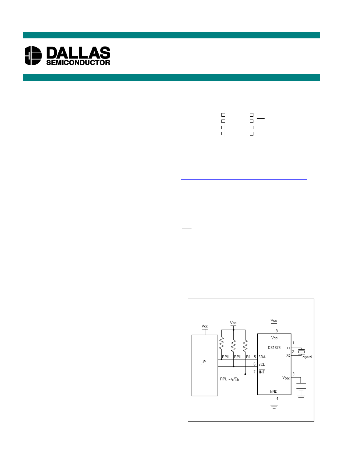
PIN ASSIGNMENT
1
X1
2
X2
3
V
BAT
GND
4
8-Pin DIP (300-mil)
8-Pin SOIC (208-mil)
Package dimension information can be found at:
http://www.maxim-ic.com/TechSupport/PackInfo.htm
Vcc
8
7
INT
6
SCL
5
SDA
PIN DESCRIPTION
V
BAT
X1 - Crystal Input
X2 - Crystal Output
INT - Interrupt Input/Output
GND - Ground
SDA - 2-wire Input/Output
SCL - 2-wire Clock Input
V
CC
- Battery Supply
- +5V Supply
TYPICAL OPERATING CIRCUIT
ORDERING INFORMATION
DS1678 8-Pin DIP (300-mil)
DS1678S 8-Pin SOIC (208-mil)
1 of 26 100101
Page 2

DS1678
DESCRIPTION
The DS1678 Real-Time Clock Event Recorder records the time and date of a non-periodic, asynchronous
event each time the INT pin is activated. The device records the seconds, minutes, hours, date, day of the
week, month, year, and century when the first event occurs. Subsequent events trigger the recording of
the 16-bit elapsed time counter (ETC) into the 2048 bytes of event log memory. This allows for up to
1025 events to be logged.
The event count register contains the total number of events that have been logged in the current eventlogging mission. The event count register also allows the user to determine if the data in the event log
memory has rolled over.
Three resolution options allow users to maximize the event log resolution while providing an adequate
maximum time between events without using extra memory locations based on the specific
characteristics of the event being logged. The seconds resolution provides the time of an event down to
the second while allowing up to 18.2 hours between events without using extra memory locations. The
minutes resolution provides the time of an event down to the minute while allowing up to 45.5 days
between events without using extra memory locations. The hours resolution provides the time of an event
down to the hour in which it occurred, while allowing up to 7.5 years between events without using extra
memory locations. Based on the expected frequency of events, the correct setting can be easily selected
to maximize the resolution and memory utilization.
The event can be triggered in three different ways depending on how the user programs the trigger select
(TRx) bits in the control register. The event can be triggered by a falling edge on the INT pin only, a
rising edge only, or it can be triggered by rising and falling edges. Triggering with both the rising and
falling edges allows for monitoring when something is turned on/off and how long it is in either state.
The RTC provides seconds, minutes, hours, day, date, month, and year information with leap-year
compensation, year 2000-compliance, and also provides an alarm interrupt. The 2-wire interface allows
the RTC to function as a stand alone RTC in the system.
The programmable alarm trip points in the RTC will allow a flag to be set in the control register when the
specified time in the alarm trip point register is reached. The flag is readable via the 2-wire interface
during an event logging mission or, when the DS1678 is not in a mission, the
INT pin will become an
output and generate an alarm interrupt if the value in the RTC equals the value in the RTC alarm register
and the duration interval select (DISx) bits are both set to zeros.
The DS1678 operates as a slave device on the 2-wire serial bus. Access is obtained by implementing a
START condition and providing a device identification code followed by a register address. All data is
transferred to and from the DS1678 most significant bit (MSB) first. The address counter will
automatically increment so that subsequent registers can be accessed sequentially until a STOP condition
is executed. When V
falls below 1.25 x V
CC
the device automatically write protects itself, terminates
BAT
any access in progress and resets the device address counter. Inputs to the device via the 2-wire bus will
not be recognized at this time to prevent erroneous data from being written to the device from an out of
tolerance system. When VCC falls below V
the device switches into a low-current battery backup
BAT
mode. Upon power-up, the device switches from battery power to VCC when VCC is greater than
+ 0.2V and recognizes inputs from the system when VCC is greater than 1.25 x V
V
BAT
by releasing
BAT
control of the write protection on the 2-wire bus.
2 of 26
Page 3

DS1678
The block diagram in Figure 1 shows the main elements of the RTC event recorder. The device has four
major components: 1) 64-bit RTC and control block, 2) 32-byte user NV RAM, 3) 2048 bytes of event
log memory (1024 events), and 4) 2-wire serial interface.
3 of 26
Page 4
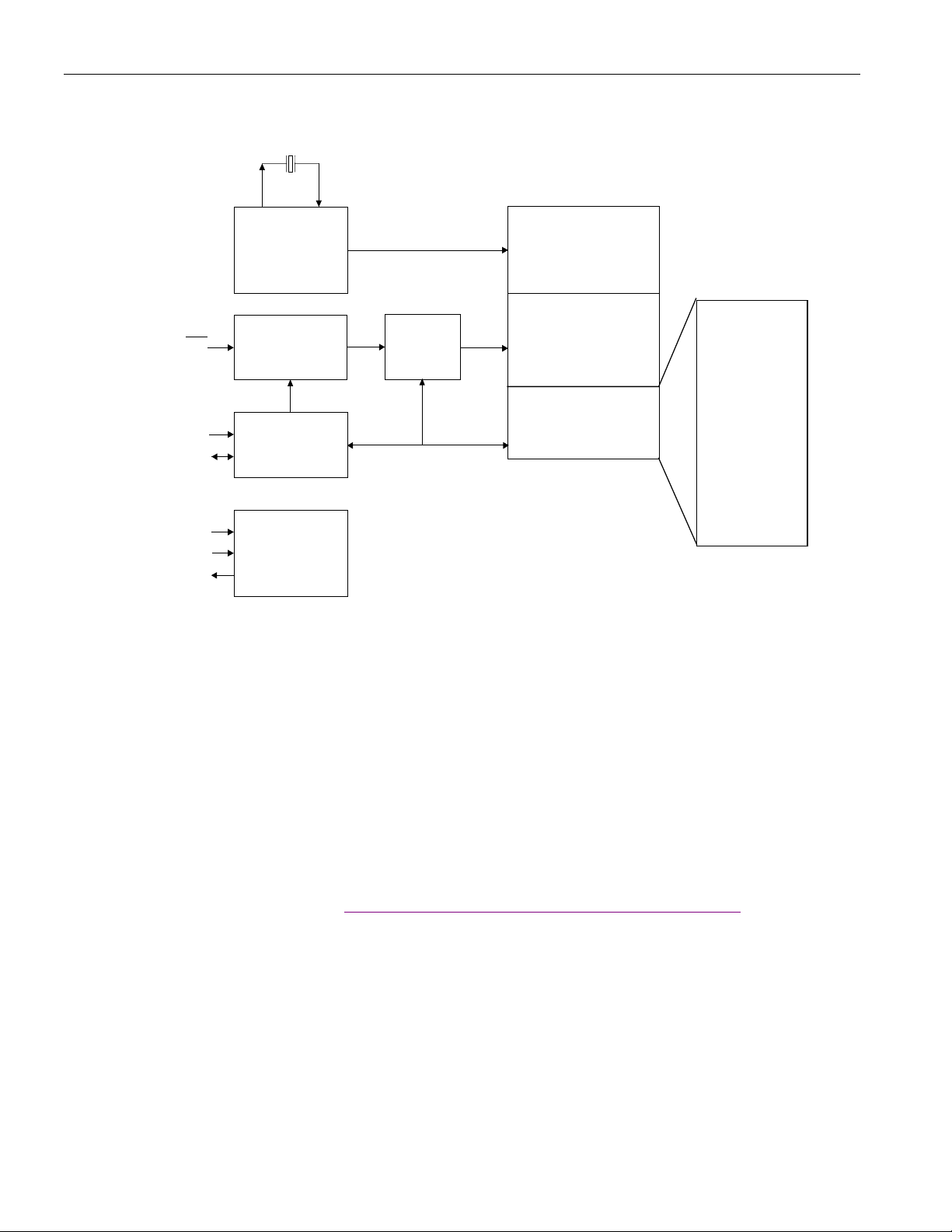
DS1678 BLOCK DIAGRAM Figure 1
A
R
2
C
T
A
R
32.768 kHz
DS1678
INT
SCL
SDA
V
C
V
BA
GND
X
OSCILLATOR
ND DIVIDE
CONTROL
LOGIC
2-WIRE SERIAL
INTERFACE
POWER
CONTROL
X1
DDRESS
REGISTE
RTC
USER
RAM
DATA LOG
RAM PORT
DATA LOG
NV SRAM
SIGNAL DESCRIPTIONS
The following paragraphs describe the function of each pin.
VCC – VCC is a +5V input supply. Communication with the DS1678 can take place only when VCC is
connected to a +5V supply.
– Battery input for standard lithium cell or other energy source. All functions of the DS1678 with
V
BAT
the exception of the serial interface circuitry are powered by V
powered by VCC when VCC > V
. If a battery or other energy source is not used, V
BAT
connected directly to ground. UL recognized to ensure against reverse charging current when used in
conjunction with a lithium battery.
See “Conditions of Acceptability” at http://www.maxim-ic.com/TechSupport/QA/ntrl.htm.
GND – Ground.
SCL (2-Wire Serial Clock Input) – The SCL pin is the serial clock input for the 2-wire synchronous
communications channel. The SCL pin is an open drain input, which requires an external pull-up resistor.
SDA (2-Wire Input/Output) – The SDA pin is the data input/output (I/O) signal for the 2-wire
synchronous communications channel. The SDA pin is an open drain I/O, which requires an external
pull-up resistor.
when VCC < V
BAT
. All functions are
BAT
should be
BAT
4 of 26
Page 5
DS1678
INT (Interrupt Input/Output) – The INT pin is an I/O that will be activated by an external device to
signify an event has occurred and should be logged. Once the pin is activated, the event will be recorded
in the event log memory and the event counter register will be incremented by one.
The INT pin can be activated in three different ways depending on how the user programs the TRx bits.
The event can be triggered by a falling edge on the INT pin only, a rising edge only, or it can be
triggered by both the rising and falling edges. By logging both the rising and falling edges as events, the
time when something is turned on and turned off can be determined and the amount of time that the
external system was in either state.
This assumes that the external system always starts logging data in a known state. For example, if a light
switch is being monitored and the switch is always in the off position before a mission is started, the first
event would be turning the lights on. The next event would have to be to turn the lights off. The time
between the events would be the amount of time the lights were in the on state. The time from turning the
lights off until the next event, which would be to turn the lights back on again, would be the amount of
time the lights were off.
The INT pin can also be used as an output when the DS1678 is not in an event logging mission. The INT
pin will become an output and generate an alarm interrupt if the DISx bits are both set to zero and the
RTC reaches the preset value in the alarm register. The INT output remains low as long as the status bit
causing the interrupt is present and the DISx bits are both set to zero.
The INT pin is an open-drain input/output with a weak internal pull-down resistor to prevent the pin
from floating if the signal connected to the pin is tri-stated. Without the resistor, the input would float
and potentially log phantom events. With the pull-down resistor, the pin can be transitioned to a low state
causing an event to be recorded if the INT pin was being held high by an outside signal that becomes tristated.
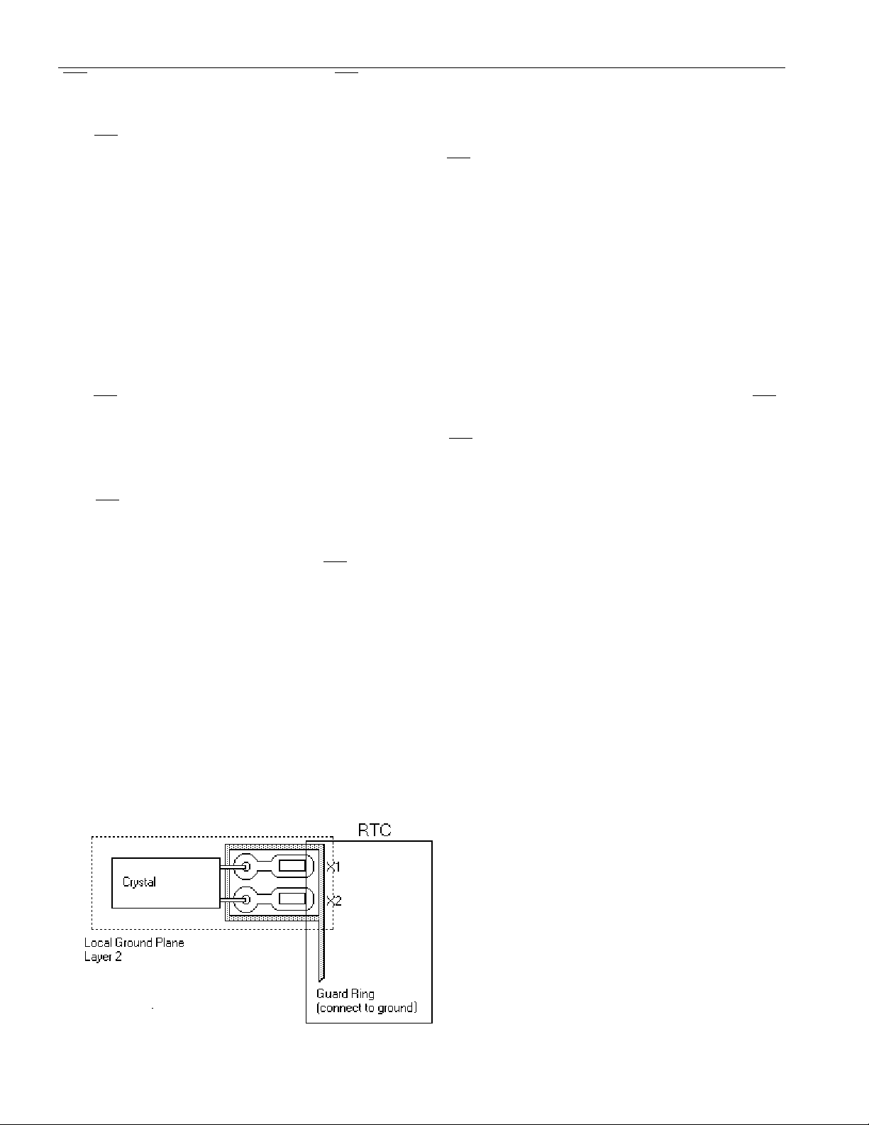
X1, X2 – Connections for a standard 32.768kHz quartz crystal, Daiwa part number DT-26S or
equivalent. For greatest accuracy, the DS1678 must be used with a crystal that has a specified load
capacitance of 12.5pF. There is no need for external capacitors or resistors. Note: X1 and X2 are very
high impedance nodes. It is recommended that they and the crystal be guard-ringed with ground and that
high frequency signals be kept away from the crystal area. For more information on crystal selection and
crystal layout considerations, please consult Application Note 58, “Crystal Considerations with Dallas
Real-Time Clocks.”
RECOMMENDED LAYOUT FOR CRYSTAL
5 of 26
Page 6

DS1678
CLOCK ACCURACY
The accuracy of the clock is dependent upon the accuracy of the crystal and the accuracy of the match
between the capacitive load of the oscillator circuit and the capacitive load for which the crystal was
trimmed. Additional error will be added by crystal frequency drift caused by temperature shifts.
External circuit noise coupled into the oscillator circuit may result in the clock running fast. See
Application Note 58, “Crystal Considerations with Dallas Real-Time Clocks” for detailed information.
MEMORY
The memory map in Figure 2a shows the general organization of the DS1678. As can be seen in the
figure, the device memory is in one contiguous segment with a data port to access the event log memory.
Since the 2-wire bus only has the capability to use one byte addressing, the DS1678 utilizes the data port
to access the 2048 bytes of event log memory. The address that the next data will be written to is stored
in the address pointer registers LSB (3Fh) and MSB (40h). These will be helpful in recovering all of the
data if a rollover occurs. The address pointer will point to the oldest event in the memory after a rollover.
This is the memory location in event log memory that would be over written by the next event. Read the
data from this point to the end of the memory and the start time stamp, including the 2-byte ETC from
last event. Working backward from the value in the start time stamp, subtract the value in the ETC from
last event to get the time the last event in the memory occurred. Then subtract the values in each of the
2-byte memory locations for elapsed time between events in order to recover the time the previous event
occurred.
The value in the ETC register LSB (3Dh) and MSB (3Eh) is the value in the actual ETC. This is the time
from the last event recorded until logging was stopped. Since a new event has not occurred, this data has
not been stored in the event memory yet.
The data port is made up of three bytes. The first byte (41h) is the event log memory address LSB, the
second byte (42h) is the event log memory address MSB, and the third byte (43h) is the event log
memory data byte. To access data via the data port, the LSB of the event log memory address is written
into 41h, the main memory address pointer will automatically increment to 42h where the event log
memory address MSB data will be written. The next transfer will indicate a read command with a 1 in
the R/
W bit of the 2-wire address byte. The data from the event log memory location corresponding to
the address written into main memory locations 41h and 42h will be available in location 43h to be read.
Any address greater than 43h will read back 00h and will not be able to be written. For address above
43h, the address pointer will increment until it reaches FFh then rollover to 00h.
The event log memory address pointer in main memory locations 41h and 42h will be auto-incremented
to the next higher event log memory address, while the pointer for the main memory will remain at
location 43h. This will allow the event log memory to be read continuously without having to write the
next desired event log memory location prior to each data read. The even address locations in the event
log memory will correspond to the LSB of the elapsed time between events and the odd memory
locations will correspond to the MSB of the elapsed time between events. For more information about
how the data is stored in the event log memory, see Figure 2b.
When the event log memory address pointer gets to the last address location (07FFh), the automatic
incrementing will stop. A new starting address will then have to be written into the event log memory
pointer bytes (41h & 42h) in order to begin reading additional data. The event log memory addresses that
can be put into the pointer (41h & 42h) are 0000h to 07FFh. The five MSB of the address are ignored.
6 of 26
Page 7

DS1678
Entering a value greater than 07FFh will result in the address location associated with the value of the
lowest 11 bits of the address.
The RTC and control registers (See Figure 2a for more detail.) are located in the main memory between
addresses 00h and 0Fh. The user NV RAM resides in locations 10h through 2Fh. The event logging
memory data port is located at locations 41h, 42h, and 43h. Memory locations 44h and up are reserved
for future extensions and will read 00h.
The end user can write only to the RTC and control registers and the user NV RAM. The rest of the
memory map is read-only from the end user’s perspective. During an event log mission, all of the
memory is read only. A write will terminate the mission. If there is an event being recorded when the
mission is terminated, the event will finish being recorded before the mission will be stopped and the
values in the MIP and ME bits will not change to 0’s until the mission has completed.
During an event log mission, memory locations 30h and above are not accessible to the user to avoid data
collisions from a user read and an event being logged at the same time. If the user tries to read a location
with an address greater than 2Fh during a mission, the value returned will be 00h.
7 of 26
Page 8
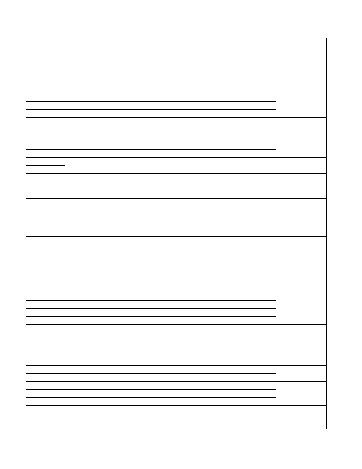
DS1678 RTC AND CONTROL PAGE Figure 2a
ADDRESS BIT 7 BIT 6 BIT 5 BIT 4 BIT 3 BIT 2 BIT 1 BIT 0 FUNCTION
00 0 10 SECONDS SECONDS
01 0 10 MINUTES MINUTES
02
03 0 0 0 0 0 DAY OF WEEK
04 0 0 10 DATE DATE
05 0 0 0 10 MO MONTH
06 10 YEAR YEAR
07 10 CENTURY CENTURY
08 MS 10 SECONDS ALARM SECONDS ALARM
09 MM 10 MINUTES ALARM MINUTES ALARM
0A MH 12/24
0B MD 0 0 0 0 DAY-OF-WEEK ALARM
0C
0D
0E ME CLR DIS1 DIS0 RO TR1 TR0 COE Control
0F 0
10
11
12
↓
2F
30 0 10 SECONDS SECONDS
31 0 10 MINUTES MINUTES
32
33 0 0 0 0 0 DAY-OF-WEEK
34 0 0 10 DATE DATE
35 0 0 0 10 MO MONTH
36 10 YEAR YEAR
37 10 CENTURY CENTURY
38 Event 0 Elapsed Time from last Event Counter LSB
39 Event 0 Elapsed Time from last Event Counter MSB
3A Low byte
3B Medium Byte
3C High Byte
3D Low Byte
3E High Byte
3F Low Address Byte
40 High Address Byte
41 Low Address Byte
42 High Address Byte
43 Data Byte
44
↓
FF
0 12/24
MEM
CLR
0 12/24
AM/PM
10 HR
AM/PM
10 HR
MIP CM LOBAT ROF 0 ALMF
AM/PM
10 HR
10 HR
10 HR HOUR ALARM
(reads 00h) Reserved
Byte 1
Byte 2
Byte 3
↓
Byte 32
10 HR
(reads 00h) Reserved
HOUR
RTC
RTC
Alarm
Status
User-
Programmable
NV Memory
HOURS
Time Stamp
And
Elapsed Time
Counter
Event Count
Elapsed Time
Counter (ETC)
Address
Pointer
Data Log
RAM
Port
DS1678
8 of 26
Page 9

DS1678
DS1678 EVENT ELAPSED TIME DURATION Figure 2b
ADDRESS REGISTER
0000 Event 1 Elapsed Time from Last Event Counter LSB
0001 Event 1 Elapsed Time from Last Event Counter MSB
0002 Event 2 Elapsed Time from Last Event Counter LSB
0003 Event 2 Elapsed Time from Last Event Counter MSB
0004
¯
07FB
07FC Event 1023 Elapsed Time from Last Event Counter LSB
07FD Event 1023 Elapsed Time from Last Event Counter MSB
07FE Event 1024 Elapsed Time from Last Event Counter LSB
07FF Event 1024 Elapsed Time from Last Event Counter MSB
¯
EVENT LOGGING
When the DS1678 event logging function is enabled, the device is said to be on an “event log mission”
until the event logging is stopped.
An event can be triggered one of three ways depending on the settings of the TRx bits in the control
register. With TR0 bit set to a 1 and TR1 bit set to a 0, the INT signal will be activated on the falling
edge of the input signal. With the TR0 bit set to a 0 and the TR1 bit set to a 1, the INT pin will be
activated on the rising edge of the input signal. With both TR0 and TR1 bits set to 1, the INT pin will be
activated on both the falling and rising edges to allow for the measurement of on/off type events and their
duration’s. If TR0 and TR1 are both set to 0, nothing will happen when the INT pin is toggled and a
mission will not start. This is an illegal state and the mission will not start without a valid value in the
TRx bits prior to attempting to start the mission.
During an event log mission, every time the INT pin is activated, the elapsed time from the last event is
written to the event log memory pages. These memory pages are accessible through the data port in the
main memory. To access data via the data port, the LSB of the address location in the event log memory
is written into 41h, the main memory address pointer will automatically increment to 42h where the
event log memory address MSB data will be written. The data from the event log memory location
corresponding to the address written into main memory locations 41h and 42h will be available in
location 43h to be read. The event log data is located at addresses 0000h to 07FFh in the event log
memory. The LSB of the first event duration is written to address location 0000h. The MSB of the first
event duration is written to address location 0001h. The LSB of the second event is written to address
location 0002h. The MSB of the second event duration is written to address location 0003h (see figure
2b for more details). Likewise, the address is incremented with each additional event duration. A total of
2048 registers have been reserved for event log data, which will allow 1024 events to be logged.
A event log mission can be initiated via two different methods (See Figure 7); by a host writing a 1 to the
MIP bit of the status register over the serial interface which automatically sets the mission enable bit in
the control register to a 1 or by activating the INT input when the mission enable bit in the control
register is set to a one. The elapsed time between events recorded during an event log mission is equal to
the value written to the event logger memory multiplied by one second, minute, or hour depending on
which one of the three is selected in the DISx bits of the control register. Writing a 0 to the MIP bit in the
Status register completes the mission and automatically writes a 0 to the ME bit in the control register
9 of 26
Page 10

DS1678
once any events that are being recorded have completed. The value in the MIP and ME bits will remain a
1 until the mission has completed, even if they are written to a 0. Upon initiation of an event log mission
by either method, the DS1678 will set the Mission-in-Progress (MIP) bit in the Control register to a one.
It should be noted that the MEM CLR bit of the Status register must be a one in order to start an event
log mission. This means that the Event Log memory, the Event Count, Elapsed Time Counter, Address
Pointer, and Start Time Stamp registers are cleared of data (all zero’s) so that an end user can not turn the
logger on and off to avoid recording events. Once the mission is stopped, the memory must be cleared in
order to start a new mission.
The time at which the first event log sample is measured is dependent upon the way the mission is
started. The first way to start a mission is with a delayed start by writing a 1 to the ME bit. The ME bit
will only be able to be written to a 1 if the MEM CLR bit is set to a 1. The mission will have a delayed
start until the first event occurs by activating the
to a one and the
INT pin is activated, the MIP bit in the status register is set to a one, the current
INT pin. If the mission starts because the ME bit is set
time/date is written to the start time stamp register, the event 0 elapsed time from last event bytes in the
time/date stamp are both written with zeros, the event count register will be incremented and the elapsed
time counter will start incrementing based on the settings in the DISx bits of the control register.
Subsequent events will be logged as the duration of time from the previous event by writing the contents
of the ETC into the event log memory when that subsequent event is triggered by the INT pin being
activated.
The second way to start a mission is write a 1 to the MIP bit of the status register over the 2-wire
interface, which will automatically write a 1 to the ME bit of the control register. This start mission
command will be ignored and no action taken if the MEM CLR bit is not set to a 1. When the MIP bit is
written to a 1 and the ME bit is set to a 1, the mission is started by loading the current time/date into the
start time stamp, the event 0 elapsed time from last event bytes in the time/date stamp are both written
with zeros, the event count register will be incremented and the elapsed time counter will start
incrementing based on the settings in the DISx bits of the control register. The first event will then be
logged as the duration of time since the start time. All subsequent events will then be logged as the
duration of time since the previous event.
The user has two options for dealing with the potential occurrence of a data overrun (i.e., more than 1024
total event logs in the event log memory) (See Figure 8). The first option is to enable the rollover feature
of the DS1678. This is accomplished by setting the rollover bit (bit 3 of the control register) to 1. When
the rollover feature is enabled, new data is written over previous data, starting with the start time stamp
register as if a new mission is starting.
The one difference with a time/date stamp from a rollover compared to a new mission start is that the two
bytes after the time/date stamp, event 0 elapsed time from last event, will have the elapsed time since
event 1024 of the event log memory. This is to allow the user to recover the information recorded prior to
the rollover. At the start of a mission, the value in these two bytes will be all zeros since there was no
previous event to have an elapsed time from.
The next event will have its elapsed time since the new time/date stamp recorded in event log memory
locations 0000h and 0001h as before. For example, if the event log memory has been completely filled
(i.e., 1024 event logs have been recorded in the event log memory) the next event will cause a new
time/date stamp to be written to the start time stamp register and the elapsed time since event 1024
10 of 26
Page 11

DS1678
written to the two event 0 elapsed time from last event registers, the subsequent event log will be written
to address locations 0000h and 0001h, and the address pointer will be incremented with each successive
data sample. When this rollover occurs, the roll over flag (ROF) in the control register will be set to one
to indicate that the memory has rolled over at least one time.
The second option for dealing with data overrun is to simply stop the recording of events after the event
log memory has been completely used. In other words, the DS1678 will stop recording event logs after
event 1025. More precisely, when the address pointer is incremented from 07FFh to 0000h after the last
memory byte is filled with a log, the DS1678 will stop recording events. This feature is enabled by
setting the Rollover bit to 0. The device will still continue monitoring the INT pin and the event counter
will continue to increment when the INT pin is activated even though the event log memory has been
filled.
It should be noted that during an event log mission, a time stamp for the first event is recorded, but is not
included for each subsequent event. However, the time of acquisition for any event is easily determined
by considering the start time, the value in the event counter register, ROF, and the address of the
particular data sample in the event log memory.
If no rollover has occurred in the event log memory (ROF = 0), the sample time associated with any
particular data point can be calculated by multiplying the sum of the elapsed time between the events up
to that event by one second, minute, or hour depending on which resolution is selected in the DISx bits of
the control register, and adding this elapsed time to the value in the start time stamp register.
If the rollover feature has been enabled, the user can determine if rollover has occurred by reading the
value in the events counter register or the ROF. The event counter register counts the total number of
events that have been acquired. If this value is greater than 0400h (decimal 1025) then the user knows
that rollover has occurred. If rollover has occurred, the user needs to determine how many times rollover
occurred in determining the sample time for any particular data sample. The address pointer will be
pointing to the oldest data in the event log memory and if the memory has rolled over at least one time,
the roll over flag will be set to 1.
As a safety measure, the DS1678 has been designed such that the end user cannot write to the event log
memory. This prevents the falsification of event log data by writing values to event log registers.
CLOCK, CALENDAR, AND ALARM
The time and calendar information is accessed by reading/writing the appropriate register bytes. Note
that some bits are set to zero. These bits will always read zero regardless of how they are written. The
contents of the time, calendar, and alarm registers are in the BCD format and are year 2000-compliant.
The DS1678 can run in either 12-hour or 24-hour mode. Bit 6 of the hour’s register is defined as the 12or 24-hour mode select bit. When high, the 12-hour mode is selected. In the 12-hour mode, bit 5 is the
AM/PM bit with logic one being PM. In the 24-hour mode, bit 5 is the second 10-hour bit (20–23 hours).
11 of 26
Page 12

DS1678
TIME-OF-DAY ALARM BITS Table 1
ALARM REGISTER MASK BITS (bit 7)
SECONDS
(MS)
1 1 1 1 ALARM ONCE PER SECOND
0 1 1 1 ALARM WHEN SECONDS MATCH
0 0 1 1 ALARM WHEN MINUTES AND SECONDS
0 0 0 1 ALARM WHEN HOURS, MINUTES, AND
0 0 0 0 ALARM WHEN DAY, HOURS, MINUTES, AND
The DS1678 also contains a time-of-day alarm. The alarm registers are located in registers 08h to 0Bh.
Bit 7 of each of the alarm registers are mask bits (See Table 1). When all of the mask bits are logic 0, an
alarm will occur once per week when the values stored in timekeeping registers 00h to 03h match the
values stored in the time-of-day alarm registers. An alarm will be generated every day when mask bit of
the day alarm register is set to 1. An alarm will be generated every hour when the day and hour alarm
mask bits are set to 1. Similarly, an alarm will be generated every minute when the day, hour, and minute
alarm mask bits are set to 1. When day, hour, minute, and seconds alarm mask bits are set to 1, an alarm
will occur every second.
MINUTES
(MM)
HOURS
(MH)
DAYS
(MD)
MATCH
SECONDS MATCH
SECONDS MATCH
As a security measure to prevent unauthorized tampering, writing to any memory location or changing
any value in the RTC and control registers will stop a event log mission and clear the MIP bit to a 0.
SPECIAL PURPOSE REGISTERS
The following description defines the operation of the special function registers of the DS1678.
CONTROL REGISTER
MSB LSB
ME CLR DIS1 DIS0 RO TR1 TR0 COE
ME - Mission Enable – This bit enables the device to begin a mission. The ME bit can not be written to
a 1 unless the MEM CLR bit in the Status register is a 1, signifying that the memory and registers have
been cleared. With the ME bit set to a one, the device will wait for the first event to occur ( INT is
activated). Once that first event occurs, the time/date stamp will be recorded in the start time stamp
register, the event 0 elapsed time from last event bytes are both written with zeros, the event count
register will be incremented, and the elapsed time count will begin incrementing to be ready with the
duration of time from the first event until the next event.
When the ME bit is set to logic 0, the DS1678 will wait until a 1 is written to the MIP bit via the 2-wire
interface to start the mission. When the MIP bit is written to a 1, the ME bit will be set to a one, the
current time/date will be recorded in the start time stamp, the event 0 elapsed time from last event bytes
are both written with zeros, the event count register will be incremented, and the elapsed time count will
begin incrementing to be ready with the duration of time from the start until the first event.
The ME bit is automatically written to a 0 whenever a mission is stopped.
12 of 26
Page 13

DS1678
CLR - Clear Enable – This bit enables the memory to be cleared. When this bit is set to a one and the
clear memory (CM) bit in the status register is subsequently written to a 1, the event log memory, event
count, and start time stamp registers are all cleared to zeros. Following the writing of a 1 to the ME bit,
the CLR bit is also cleared to zero. If the clear enable bit is set, but a command other than writing a 1 to
the clear memory bit is issued next, the CLR bit is cleared to a zero and the contents of the event log,
start time stamp, and event counter register are unchanged.
DIS1, DIS0 - Duration Interval Select [0-1] – These bits select the amount of time between increments
of the elapsed time counter that is used to determine the amount of time between events. After the first
event is recorded, all subsequent events are recorded as the elapsed time since the previous event. When
a subsequent event occurs, the ETC value is stored in the event log memory.
In order to obtain the maximum accuracy of the event logger, the smallest possible resolution of the ETC
should be selected. The expected maximum time between events must also be taken into account in order
to get the full 1025 events logged because when the ETC count reaches 65535 increments, if the next
event has not occurred by that point in time, FFh will be written into the memory, the ETC will roll over
to 00h and continue to count until the next event occurs or FFh is reached again. Whenever FFh is
reached by the ETC, it will store that value in event log memory, reset to 00h, continue counting, and the
memory address pointer will increment to the next memory location. When ever an FFh appears in the
memory, the next two bytes of data will be part of the elapsed time for the same event, even if the value
in the next two bytes of memory are 00h which means that an event occurred at time increment FFh. In
order to recover the total elapsed time between events when a FFh is in the Event Log Memory; simply
add the contents of the next two bytes to the FFh. If the next two bytes are 00h indicating that the event
occurred at FFh, by adding the 00h in the next two bytes, you will end up with FFh. If the next two bytes
are 01h, you will get 100h when the data is added to FFh. This will represent the total elapsed time since
the previous event. The event counter will not be incremented when the ETC rolls over since a new event
has not occurred.
The ETC will be incremented as the selected single seconds, minutes, or hours byte of the RTC
increments to prevent time losses from short duration events. Since the time base in the RTC continues to
run, even when the ETC is cleared to prepare for a new event, and the ETC is incremented every time the
selected byte in the RTC increments, the actual time resolution will not be lost even when events occur
more frequently than the minimum time resolution selected. If an event occurs half way between
increments of the ETC, then the first increment of the next event will occur when the seconds, minutes or
hours register increments next, thus preserving the correct time to the resolution selected in the DISx bits.
The user can select one of the settings in Table 2.
When the Alarm Interrupt Output is to be used, the DISx bits should be set to zeros, which will disable
the ETC and the rest of the event logger circuitry to conserve battery life. An event-logging mission can
not be started if the DISx bits are both set to zero. This will enable the Alarm Flag to generate an Alarm
Interrupt via the
INT output pin.
With the DIS0 bit set to a one and the DIS1 bit set to zero, the ETC will increment every time the single
seconds byte in the RTC is incremented. This will give the maximum resolution between events, but
since the counter is limited to only 16 bit and will roll over to the next two memory bytes when it reaches
the maximum value, the largest interval between events that can be accurately measured without using
additional memory space and reducing the total number of events able to be logged is 65,535 seconds or
about 18.2 hours. If the maximum time between events could be greater than 18.2 hours, you should
consider using one of the courser resolutions to conserve memory.
13 of 26
Page 14

DS1678
With the DIS0 bit set to a zero and the DIS1 bit set to a one, the ETC will increment every time the
single minutes byte in the RTC is incremented. This will give a medium resolution between events, but
will increase the largest possible interval between events that can be accurately measured without using
additional memory space and reducing the total number of events able to be logged to 65,535 minutes or
about 45.5 days. If the maximum time between events could be greater than 45.5 days, you should
consider using one of the courser resolutions to conserve memory.
With both of the DISx bits set to a one, the ETC will increment every time the single hours byte in the
RTC is incremented. This will give the lowest resolution between events, but will increase the largest
possible interval between events that can be accurately measured without using additional memory space
and reducing the total number of events able to be logged to 65,535 hours or about 7.5 years.
In the event that a second event occurs before the ETC is able to increment for the first time, all zeros
will be logged in the event log memory and the ETC will be reset. If this occurs, the time base will
remain correct since it is based on the separate RTC incrementing, but the exact time of the event will be
no more accurate than the size of the time increment that is chosen. For this reason, it is recommended to
use the finest resolution possible for your logging to minimize the errors. If the normal duration between
events is several days or months, then a few minutes or an hour may not be significant to your data
accuracy.
As an example, an event occurs after 28h hours which causes the ETC to be reset. The ETC is set to
increment on the hour, but the next event happens after 45 minutes. The value recorded in the event log
memory is 00h, the event counter is incremented, and the ETC is cleared to begin counting for the next
event. That next event happens 20 minutes later, but the value in the ETC is 01h because the RTC
incremented the ETC on the hour, which was 15 minutes after the last event was recorded in the event
log memory. We now know that in the course of about an hour three events took place. If this is normal,
then we should have chosen a finer resolution, but this does sometimes happen, even when events are
normally spread widely apart. We did not loose any data in our example because we know in which hour
the events took place and when we chose the resolution, we decided that knowing which hour was
accurate enough for our needs. The RTC maintained the correct time base, even though the ETC was
cleared before it was incremented even once for the second event in our example. The third event
incremented after only 15 minutes, but, relative to the first event in our example, this was correct because
the second event occurred after 45 minutes, and the third event was incremented after an additional
15 minutes, which makes one hour.
DURATION INTERVAL SELECT BITS Table 2
DIS1 DIS0 ELAPSED TIME COUNT
RESOLUTION
0 0 Alarm Interrupt Output Enabled
0 1 The Counter will Increment Every Second 18.2 Hours
1 0 The Counter will Increment Every Minute 45.5 Days
1 1 The Counter will Increment Every Hour 7.5 Years
RO - Roll-Over – This bit determines whether the datalog function of the DS1678 rolls over or stops
writing data to the event log memory if the event log memory is completely filled. If RO is set to a 1, the
event log memory will “roll over” after all 2048 bytes in the event log memory have been used. In other
words, after the 1024th event recorded in the event log memory, the following sample will have the full
time/date stamp information written to the start time stamp register and the contents of the ETC written to
the 2-byte following the start time stamp (event 0 elapsed time from last event) and the next sample will
have the duration of time from the new start time stamp value written to event log memory address
14 of 26
MAX. TIME BETWEEN
EVENTS
Page 15

DS1678
locations 0000h and 0001h, overwriting the original data. Likewise, subsequent samples will increment
through the event log registers, overwriting their data.
The event 0 elapsed time from last event bytes will have the elapsed time since the last event in the event
log memory. This is to allow the user to recover the information prior to the rollover. At the start of a
mission, the value in these 2 bytes will be all zeros since there was no previous event from which to have
an elapsed time.
If RO is set to a 0, no further event logs will be written to the event log memory after all event log
memory registers have been filled. Events, however, will continue to be recognized and the Event Count
register will be incremented for each event. Likewise, the RTC alarm flag will also continue to function.
TR1, TR0 - Trigger Select [1,0] – This bit selects the edge(s) that will activate the INT pin to cause an
event to be logged. An event can be triggered one of three ways depending on the settings of the TRx bits
in the control register. With TR0 bit set to a 1 and TR1 bit set to a 0, the
the falling edge of the input signal. With the TR0 bit set to a 0 and the TR1 bit set to a 1, the
INT signal will be activated on
INT pin will
be activated on the rising edge of the input signal.
With both TR0 and TR1 bits set to 1, the INT pin will be activated by both the rising and falling edges to
allow for the measurement of on/off type events and their durations. If TR0 and TR1 are both set to 0,
nothing will happen when the INT pin is toggled and a mission will not start. This is an illegal state and
the mission will not start without a valid value in the TRx bits prior to attempting to start the mission.
TRIGGER SELECT BITS Table 3
TR1 TR0 EDGE(S) USED TO TRIGGER AN EVENT
0 0 Nothing, Illegal State
0 1 Falling Edge
1 0 Rising Edge
1 1 Both Rising and Falling Edges
COE - Clock Oscillator Enable – This bit allows the clock oscillator to be shut off to save power. The
RTC will no longer keep time when the oscillator is shut off, but the information stored in the device
memory will be maintained. An event log mission can not start with COE set to zero and the RTC must
be reset to the correct value after the oscillator is restarted and prior to starting a mission in order to
obtain good data. A clear memory can also not be executed without the oscillator running. When VCC >
V
, the oscillator will automatically start, no matter what the value in the COE bit to allow proper
BAT
communications. This is a way to preserve the data longer in battery mode once a mission has been
completed in order to increase the battery life and thus the data integrity lifetime.
STATUS REGISTER
MSB LSB
0MEM CLRMIP CMLOBATROF 0 ALMF
MEM CLR - Memory Cleared – This bit indicates that the event log memory, event count, and start
time stamp registers are all cleared to zero. MEM CLR is cleared to zero when an event log mission is
started (i.e., MIP = 1).
15 of 26
Page 16

DS1678
MIP - Mission in Progress – This bit indicates the sampling status of the DS1678. If MIP is logic 1, the
device is currently on a “mission” in which it is operating in the event logging mode. The MIP bit is
changed to logic 1 immediately following the activation of the INT pin if the ME bit of the control
register contains a 1. In order to immediately start an event logging mission via the 2-wire bus, a 1 can be
written into the MIP bit and a 1 will automatically be written into the ME bit of the control register.
If MIP is logic 0, the DS1678 is not currently in event logging mode. The MIP bit transitions from logic 1
to logic 0 whenever event logging is stopped. Event logging is stopped when the DS1678 is cleared by
writing to the clear enable and memory clear bits or when any memory location including the RTC or
control registers are written to during a mission. The MIP bit can also be written to logic 0 by the end user
to stop event logging via the 2-wire bus. By writing a 0 to the MIP bit and stopping the mission, a 0 is
automatically written to the ME bit of the control register. It cannot, however, be written to logic 1 to start
a mission unless the MEM CLR bit is a 1 to signify that the memory has been cleared.
CM - Clear Memory – This bit will trigger the memory to be cleared if the CLR clear enable and COE
clock oscillator enable bits in the control register are set to a 1. This will cause the event log memory,
event count, and start time stamp registers to all be cleared to zeros. Once the memory has been cleared,
the CLR enable bit and the CM bits will be set to zeros and the MEM CLR bit will be set to a 1 to allow a
new mission to begin. Clearing the memory is a two-write process to reduce the risk of accidentally
erasing the memory. The CLR bit must be set to a 1 before the CM bit can be written to a 1. During the
clear memory operation the DS1678 should not be accessed for 500µs while the memory is erased. The
MEM CLR bit should read a 1 before trying to access the cleared memory or registers.
LOBAT - Low Battery Flag – This bit reflects the status of the backup power source connected to the
V
pin. A logic 1 for this bit indicates an exhausted lithium energy source.
BAT
ROF - Roll Over Flag – This bit will be set to a one if the RO bit of the control register is set to a one,
the last data log memory location has been filled and a new event has occurred, which will cause the
time/date stamp to be over written. If RO is set to a 0 (roll over is disabled), the last data log memory
location has been filled and an new event has occurred, ROF will be set to a 1 to indicate that more events
have occurred than the number of available memory locations. The event counter will continue to record
events, even after the event log memory is full. The ROF is cleared by the clear memory command.
ALMF - Alarm Flag – A logic 1 in the alarm flag bit indicates that the current time has matched the
time-of-day alarm registers. If at the same time, the DISx bits are both logic 0’s, the
INT pin will go low
to issue an alarm interrupt. ALMF is a read only bit and is cleared by accessing any of the Alarm register
bytes either with a read or a write. Writing any memory location during a mission will stop the mission. A
mission can not be started when the DISx bits are both set to 0.
EVENT COUNTER
This 3-byte register set provides the number of events that have been logged during the current data
logging operation (also known as a “mission”). The contents of this register can be used by software to
point to the most recent data sample in the event log memory. The data in these registers are cleared when
the event log memory is cleared. The event counter is not incremented when the ETC reaches FFh and
rolls over to the next 16 bits of memory.
ADDRESS POINTER REGISTER
The address pointer register always contains the address that the next data LSB will be written to in the
event log memory. The address pointer registers are located in the main memory map at LSB (3Fh) and
16 of 26
Page 17

DS1678
MSB (40h). These will be helpful in recovering all of the data if a rollover occurs. The address pointer
will point to the oldest event in the memory after a rollover. This is the memory location that would be
over written by the next event. Read the data from this point to the end of the memory and the start time
stamp including the 2-byte ETC from last event in order to recover all of the data in the correct order.
GLITCH CONTROL CIRCUIT
The DS1678 has a built-in glitch control circuit to filter noise on the INT pin from triggering false events.
A minimum of one internal clock cycle (0.122ms) up to a maximum of two internal clock cycles
(0.245ms) are required to recognize a transition on the input as an event. An event then requires an
additional six to eight internal clock cycles (0.752ms to 0.977ms) to be processed and recorded into
memory. This means that the minimum event occurrence that can be recognized by the DS1678 requires
seven to 10 internal clock cycles (0.854ms to 1.22ms). Failure to ensure this timing will cause the event
to be ignored. Thus, it is recommended that you design with the maximum timing specs.
The INT pin has a weak internal pull-down resistor to prevent the pin from floating if the signal
connected to the pin is tri-stated. Without the resistor, the input would float and potentially log phantom
events. With the pull-down resistor, the pin can be transitioned to a low state causing an event to be
recorded if the INT pin was being held high by an outside signal that becomes tri-stated.
SECURITY
The DS1678 provides several measures to insure data integrity for the end user. These security measures
are intended to prevent third-party intermediaries from tampering with the data that has been stored in the
event log memory.
As a first security measure, the event log memory is read-only from the perspective of the end user. The
DS1678 can write the data into these memory banks, but the end user cannot write data to individual
registers. This prevents an unscrupulous intermediary from writing false data to the DS1678. The end
user, however, can clear the contents of the event log memory. A new mission can not be started unless
the MEM CLR bit has been set to a 1 to indicate that the memory and registers are cleared.
As a second security measure, changing any value in the memory including the RTC and control registers
will stop event logging and clear the MIP and ME bits. The MEM CLR bit must be set to 1 so that the
memory and registers are cleared before a new event log mission can begin.
POWER CYCLING
When VCC falls below 1.25 x V
progress and resets the device address counter. Inputs to the device via the 2-wire bus will not be
recognized at this time to prevent erroneous data from being written to the device from an out of tolerance
system. When V
falls below V
CC
power-up, the device switches from battery power to VCC when VCC is greater than V
recognizes inputs from the system when V
protection on the 2-wire bus.
the device automatically write protects itself, terminates any access in
BAT
the device switches into a low-current battery backup mode. Upon
BAT
+ 0.2V and
BAT
is greater than 1.25 x V
CC
by releasing control of the write
BAT
2-WIRE SERIAL DATA BUS
The DS1678 supports a bi-directional, 2-wire bus and data transmission protocol. A device that sends
data onto the bus is defined as a transmitter, and a device receiving data as a receiver. The device that
controls the message is called a “master.” The devices that are controlled by the master are “slaves.” The
bus must be controlled by a master device that generates the serial clock (SCL), controls the bus access,
17 of 26
Page 18

DS1678
and generates the START and STOP conditions. The DS1678 operates as a slave on the 2-wire bus.
Connections to the bus are made via the open-drain I/O lines SDA and SCL.
The following bus protocol has been defined (See Figure 3):
§ Data transfer may be initiated only when the bus is not busy.
§ During data transfer, the data line must remain stable whenever the clock line is HIGH. Changes in
the data line while the clock line is high will be interpreted as control signals.
Accordingly, the following bus conditions have been defined:
Bus not busy: Both data and clock lines remain HIGH.
Start data transfer: A change in the state of the data line, from HIGH to LOW, while the clock is HIGH,
defines a START condition.
Stop data transfer: A change in the state of the data line, from LOW to HIGH, while the clock line is
HIGH, defines the STOP condition.
Data valid: The state of the data line represents valid data when, after a START condition, the data line
is stable for the duration of the HIGH period of the clock signal. The data on the line must be changed
during the LOW period of the clock signal. There is one clock pulse per bit of data.
Each data transfer is initiated with a START condition and terminated with a STOP condition. The
number of data bytes transferred between START and STOP conditions is not limited, and is determined
by the master device. The information is transferred byte-wise and each receiver acknowledges with a
ninth bit. Within the bus specifications a regular mode (100kHz clock rate) and a fast mode (400kHz
clock rate) are defined. The DS1678 works in both modes.
Acknowledge: Each receiving device, when addressed, is obliged to generate an acknowledge after the
reception of each byte. The master device must generate an extra clock pulse which is associated with this
acknowledge bit.
A device that acknowledges must pull down the SDA line during the acknowledge clock pulse in such a
way that the SDA line is stable LOW during the HIGH period of the acknowledge related clock pulse. Of
course, setup and hold times must be taken into account. A master must signal an end of data to the slave
by not generating an acknowledge bit on the last byte that has been clocked out of the slave. In this case,
the slave must leave the data line HIGH to enable the master to generate the STOP condition.
18 of 26
Page 19

DS1678
Figure 4 details how data transfer is accomplished on the 2-wire bus. Depending upon the state of the
R/ W bit, two types of data transfer are possible:
1. Data transfer from a master transmitter to a slave receiver. The first byte transmitted by the
master is the slave address. Next follows a number of data bytes. The slave returns an acknowledge
bit after each received byte.
2. Data transfer from a slave transmitter to a master receiver. The first byte (the slave address) is
transmitted by the master. The slave then returns an acknowledge bit. Next follows a number of data
bytes transmitted by the slave to the master. The master returns an acknowledge bit after all received
bytes other than the last byte. At the end of the last received byte, a “not acknowledge” is returned.
The master device generates all of the serial clock pulses and the START and STOP conditions. A
transfer is ended with a STOP condition or with a repeated START condition. Since a repeated START
condition is also the beginning of the next serial transfer, the bus will not be released.
The DS1678 may operate in the following two modes:
1. Slave receiver mode (DS1678 write mode): Serial data and clock are received through SDA and
SCL. After each byte is received, the receiver transmits an acknowledge bit. START and STOP
conditions are recognized as the beginning and end of a serial transfer. The slave address byte is the
first byte received after the start condition is generated by the master. The address byte contains the 7-
bit DS1678 address, which is 1001010, followed by the direction bit (R/ W ), which is 0. The second
byte from the master is the register address. This sets the register pointer. If the write is being done to
set the register pointer, a STOP or repeated START may then be sent by the master. Otherwise, the
master then transmits each byte of data, with the DS1678 acknowledging each byte received. The
master will generate a stop condition to terminate the data write (See Figure 4).
2.
Slave transmitter mode (DS1678 read mode): The first byte is received and handled as in the slave
receiver mode. However, in this mode, the direction bit will indicate that the transfer direction is
reversed. Serial data is transmitted on SDA by the DS1678 while the serial clock is input on SCL. The
slave address byte is the first byte received after the start condition is generated by the master. The
address byte contains the 7-bit DS1678 address, which is 1001010, followed by the direction bit
(R/
W ), which is 1. After receiving a valid slave address byte and direction bit, the DS1678 generates
an acknowledge on the SDA line. The DS1678 begins to transmit data on each SCL pulse starting
with the register address pointed to by the register pointer. As the master reads each byte, it must
generate an acknowledge. The DS1678 must receive a “not acknowledge” on the last byte to end a
read (See Figure 4).
19 of 26
Page 20

DS1678
ABSOLUTE MAXIMUM RATINGS*
Voltage on Any Pin Relative to Ground -0.3V to +6V
Operating Temperature -40°C to +85°C
Storage Temperature -55°C to +125°C
Soldering Temperature See J-STD-020A specification
* This is a stress rating only and functional operation of the device at these or any other conditions above
those indicated in the operation sections of this specification is not implied. Exposure to absolute
maximum rating conditions for extended periods of time may affect reliability.
RECOMMENDED DC OPERATING CONDITIONS (-40°C to +85°C)
PARAMETER SYMBOL MIN TYP MAX UNITS NOTES
Power Supply Voltage V
Input Logic 1 V
Input Logic 0 V
Battery Voltage V
CC
IH
IL
BAT
4.5 5.0 5.5 V
2.2 VCC + 0.3 V
-0.3 +0.8 V
2.6 3.5 V
DC ELECTRICAL CHARACTERISTICS (-40°C to +85°C)
PARAMETER SYMBOL MIN TYP MAX UNITS NOTES
Input Leakage I
Logic 0 Output
I
= 4mA
OL
V
LI
OL
-1 +1
0.4 V
mA
Output Current 0.4V
Active Supply Current I
Battery Standby Current
CCA
I
OSC
12mA
300 500 nA
(Oscillator On)
Battery Standby Current
I
BAT
50 150 nA
(Oscillator Off)
Power-Fail Voltage V
PF
1.216 x V
BAT
1.25 x V
BAT
1.284 x V
BAT
V6
AC ELECTRICAL CHARACTERISTICS (-40°C to 85°C, VCC= 2.6V to 5.5V)
PARAMETER SYMBOL MIN TYP MAX UNITS NOTES
Input Capacitance C
Crystal Capacitance C
Minimum Signal Width t
Minimum Event Rate t
GLITCH
EVENT
I
X
10 pF
12.5 pF
0.122 0.245 ms
0.854 1.22 ms
20 of 26
Page 21

DS1678
AC ELECTRICAL CHARACTERISTICS (-40°C to +85°C, VCC = 4.5V to 5.5V)
PARAMETER SYMBOL CONDITION MIN TYP MAX UNITS NOTES
SCL Clock Frequency f
Bus Free Time
t
Between a STOP and
START Condition
Hold Time (Repeated)
t
hd:sta
START Condition.
LOW Period of SCL t
HIGH Period of SCL t
Set-Up Time for a
high
t
su:sta
Repeated START
Data Hold Time t
Data Set-up Time t
hd:dat
su:dat
Rise Time of Both
SDA and SCL Signals
Fall Time of Both
SDA and SCL Signals
Set-up Time for STOP t
Capacitive Load for
su:sto
C
Each Bus Line
Input Capacitance C
scl
buf
low
t
r
t
f
Fast Mode
Standard Mode
Fast Mode
Standard Mode
Fast Mode
Standard Mode
Fast Mode
Standard Mode
Fast Mode
Standard Mode
Fast Mode
Standard Mode
Fast Mode
Standard Mode
Fast Mode
Standard Mode
Fast Mode
Standard Mode
Fast Mode
Standard Mode
Fast Mode
Standard Mode
b
i
100 400
100
1.3
4.7
0.6
4.0
1.3
4.7
0.6
4.0
0.6
4.7
0
0
100
250
20 +
0.1C
20 +
0.1C
b
b
300
1000
300
300
0.6
4.0
400 pF 4
5pF
kHz
µs
µs 1
µs
µs
µs
0.9 µs 2
ns 3
ns 4
ns 4
µs
DATA TRANSFER ON 2-WIRE SERIAL BUS Figure 3
SDA
SCL
START
CONDITION
MSB
12 6789
slave address
R/W
direction
bit
acknowledgement
signal from receiver
12 89
ACK ACK
21 of 26
3 - 8
repeated if more bytes
are transferred
acknowledgement
signal from receiver
STOP CONDITION
OR
REPEATED
START CONDITION
Page 22

2-WIRE SERIAL COMMUNICATION WITH DS1678 Figure 4
S
Write to Memory Address Pointer
SCL
A2
SDA
0W1S 1 0 A1 A000 A A P
1
A3A4A5A6A7
DS1678
Device Address Byte Memory Address ByteStart
DS16 78
ACK
Write to Memory Location (Single Byte)
SCL
SDA
1S 1 0 A1 A000 A
Device Address Byte Mem ory Address ByteStart
1
0W
DS16 78
ACK
Read Single Byte from C urrent Memory Address Pointer Location
SCL
SDA
1S 1 1000 Rd A N P
Device Address Byte Da ta B yteStart
DS16 78
ACK
Read Mu ltip le Bytes from C urrent Memory Ad dress Pointer Location
SCL
SDA
1S 1 10 D000 Rd A A
Start
Device Address Byte Most Significant
DS16 78
ACK
Da ta B yte
Read Single Byte from New Mem ory Address Po inter Location
SCL
SDA
1S 1 000 A A
Device Address Byte Memory Address ByteStart
10W 0
DS16 78
ACK
SCL
NP
SDA
D7
D1D2D3D4D5D6 D0
DS1678
Stop
ACK
A2A3A4A5A6A7
A2A3A4A5A6A7
A
DS1678
ACK
D1D2D3D4D5D6D70 D0
NACK
D1D2D3D4D5D6D7 NP
Master
ACK
A1 A0
DS16 78
ACK
Data Byte
StopMaster
Least Significant
Data Byte
1R 1 1000 Rd A
Repeated
Start
Device Address
Byte
D1D2D3D4D5D6D7
D1D2D3D4D5D6D70 D0
D0
DS1678
ACK
NACK
AP
Stop
StopMaster
DS16 78
ACK
Data Byte StopMaster
NACK
2-WIRE COMMUNICATION TIMING DIAGRAM Figure 5
SDA
t
BUF
t
HD:STA
TART
SCL
STOP
START
t
t
HD:STA
LOW
t
R
t
HD:DAT
t
HIGH
t
F
t
t
SU:DAT
SU:STA
REPEATED
t
SU:STO
22 of 26
Page 23

EVENT RECOGNITION TIMING DIAGRAM Figure 6a
Good Events
t
EVENT
t
/INT
GLITCH
Transition Point
DS1678
Event 1
Event 2
Bad Event 1
t
/INT
GLITCH
Transition Point
Bad Event 2
t
/INT
Event 1
Event 2
EVENT
Transition Point
is missed
EVENT RECOGNITION TIMING DIAGRAM Figure 6b
Good Events
t
EVENT
t
/INT
GLITCH
Transition Point
Bad Event 1
/INT
Bad Event 2
/INT
Event 1 Event 2
t
GLITCH
Event 1
Event 2
is missed
Transition Point
t
EVENT
Transition Point
23 of 26
Page 24

START MISSION FLOW CHART Figure 7
y
DS1678
Start via
Computer
Mem Clr =1
yes
Write a 1 to
the MIP bit
The ME bit is
Automatically
Written to a 1
Time/Date Stamp
is Written
no
Clear
Memory
Start via
External Event
Mem Clr =1
yes
Write a 1 to
the ME bit.
MIP = 0
INT Input
Activated
yes
no
no
Clear
Memory
Continue to
Monitor Input
ETC Starts
Incrementing
EC is
Incremented
INT Input
Activated
yes
Record Event in
Event Memory
ETC is
Cleared
no
Continue to
Monitor Input
MIP Automaticall
Written to a 1
Time/Date Stamp is
Written
ETC Starts
Incrementing.
EC is
Incremented
INT Input
Activated
yes
Record Event in
Event Memory
no
Continue to
Monitor Input
ETC is
Cleared
24 of 26
Page 25

ROLL OVER FLOW CHART Figure 8
y
EC is
Incremented
DS1678
INT Input
Activated
Memor
Full
Rollover
Enable = 1
yes
yes
yes
no
no
no
Continue to
Monitor Input
Record Event in
Event Memory
ETC Written to Event 0
and
Time/Date Stamp
is Written
ETC is
Cleared
25 of 26
Page 26

DS1678
NOTES:
1. After this period, the first clock pulse is generated.
2.
A device must initially provide a hold time of at least 300ns for the SDA signal in order to bridge the
undefined region of the falling edge of SCL. The maximum t
not stretch the LOW period (t
3.
A fast mode device can be used in a standard mode system, but the requirement t
) of the SCL signal.
low
then be met. This will automatically be the case if the device does not stretch the LOW period of the
SCL signal. If such a device does stretch the LOW period of the SCL signal, it must output the next
data bit to the SDA line t
4.
C
– Total capacitance of one bus line in pF.
B
5.
t
and tF are measured with a 1.7kΩ pull-up resistor, 200pF pull-up capacitor, 1.7kΩ pull-down
R
r MAX
+ t
= 1000 + 250 = 1250ns before the SCL line is released.
su:dat
resistor and 5pF pull-down capacitor.
6.
V
measures at V
pf
BAT
= 3.0V.
has only to be met if the device does
hd:dat
> 250ns must
su:dat
26 of 26
 Loading...