

Page 1
DS1667
DS1667
Digital Resistor with OP AMP
FEATURES
• Two digitally controlled 256-position potentiometers
• Serial port provides means for setting and reading
both potentiometers
• Resistors can be connected in series to provide addi-
tional resolution
• Default wiper position on power up is 50%
• Resistive elements are temperature compensated to
20% end to end
+
• Two high gain wide bandwidth operational amplifiers
• Low power CMOS design
• Applications include analog–to–digital and digital–to–
analog converters, variable oscillators, and variable
gain amplifiers
• 20–pin DIP package or optional 20–pin SOIC surface
mount package
• Operating temperature range of 0°C to 70°C
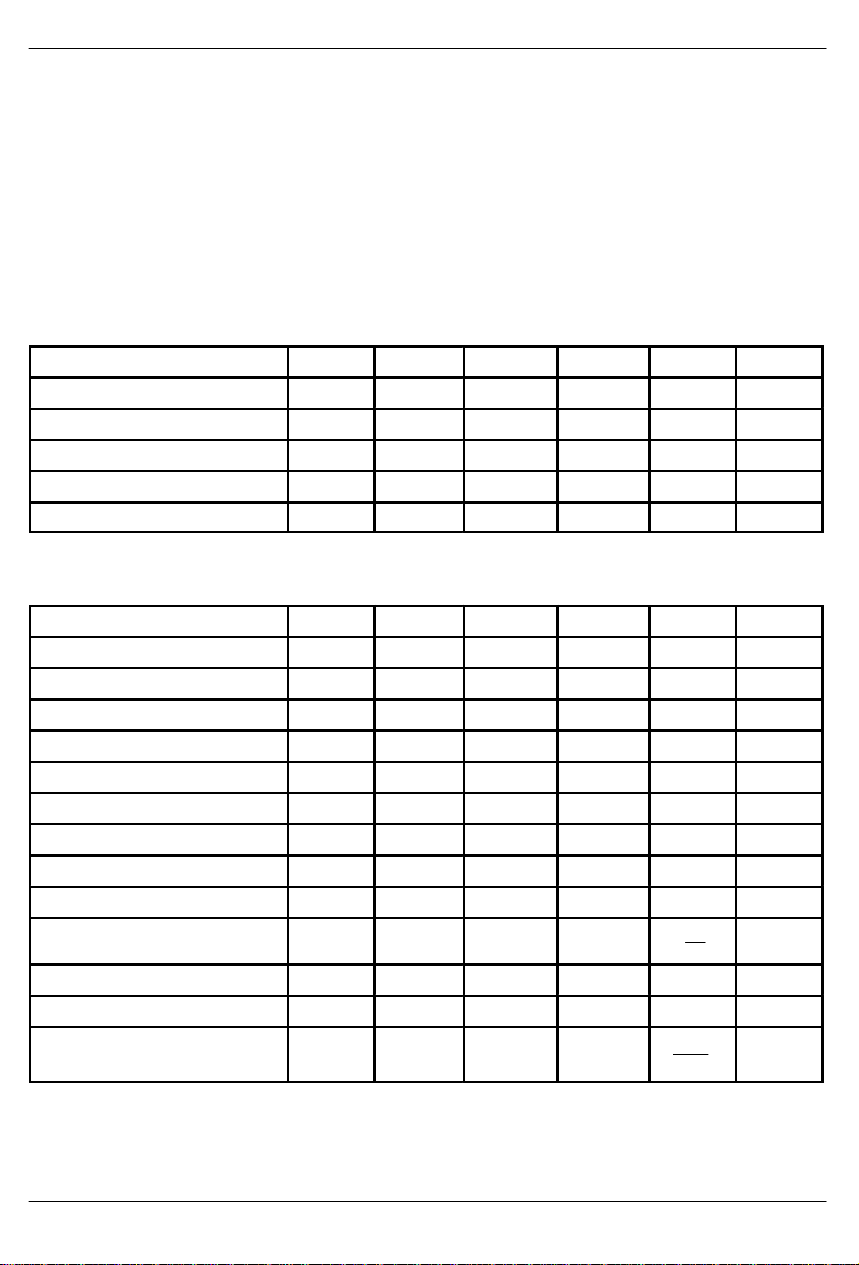
• Resistance Values
DS1667-10: 10K 39 ohms 1.1 MHz
DS1667-50: 50K 195 ohms 200 kHz
DS1667-100: 100K 390 ohms 100 kHz
DESCRIPTION
The DS1667 is a dual–solid state potentiometer that is
adjustable by digitally selected resistive elements.
Each potentiometer is composed of 256 resistive elements. Between each resistive section of each potentiometer are tap points accessible to the wiper. The position of the wiper on the resistive array is set by an 8–bit
register that controls which tap point is connected to the
wiper output. Each 8–bit register can be read or written
by sending or receiving data bits over a 3–wire serial
port. In addition, the resistors can be stacked such that
RESOLUTION -3 dB POINT
PIN ASSIGNMENT
NINV0
OUT1
1
2
INV0
3
V
B
4
W1
5
H1
6
L1
7
RST
8
CLK
9
10
GND
20-Pin DIP (300 Mil) and 20-Pin SOIC
20
V
CC
19
OUT0
18
SOUT
17
W0
16
H0
15
L0
14
COUT
13
DQ
12
INVI
11
NINVI
PIN DESCRIPTION
V
CC
GND - Ground
L0, L1 - Low End of Resistor
H0, H1 - High End of Resistor
W0, W1 - Wiper End of Resistor
V
B
SOUT - Wiper for Stacked
RST
DQ - Serial Port Input/Output
CLK - Serial Port Clock Input
COUT - Cascade Serial Port Output
NINV0, NINVI - Noninverting OP AMP Input
INV0, INVI - Inverting OP AMP Input
OUT0, OUT1 - OP AMP Outputs
a single potentiometer of 512 sections results. When
two separate potentiometers are used, the resolution of
the DS1667 is equal to the resistance value divided by
256. When the potentiometers are stacked end to end,
the resistance value is doubled while the resolution remains the same. The DS1667 also contains two high
gain wide bandwidth operational amplifiers. Each amplifier has both the inverting and non-inverting inputs
and the output available for user configuration. The operational amplifiers can be paired with the resistive ele-
- +5 Volt Supply
- Substrate Bias and OP AMP
Negative Supply
Configuration
- Serial Port Reset Input
Copyright 1995 by Dallas Semiconductor Corporation.
All Rights Reserved. For important information regarding
patents and other intellectual property rights, please refer to
Dallas Semiconductor databooks.
021492 1/11
Page 2
DS1667
ments to perform such functions as analog to digital
conversion, digital to analog conversion, variable gain
amplifiers, and variable oscillators.
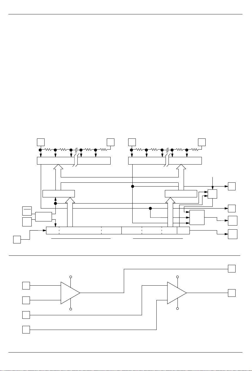
OPERATION - DIGITAL RESISTOR SECTION
The DS1667 contains two potentiometers, each of
which has its wiper set by a value contained in an 8 bit
register (see Figure 1). Each potentiometer consists of
256 resistors of equal value with tap points between
each resistor and at the low end.
In addition, the potentiometer can be stacked by connecting them in series such that the high end of poten-
BLOCK DIAGRAM Figure 1
RESISTOR SECTION
L0 H0 L1 H1
256–TO–1 MULTIPLEXER 256–TO–1 MULTIPLEXER
WIPER 0–8 BITS WIPER 1–8 BITS
tiometer 0 is connected to the low end of potentiometer
1. When stacking potentiometers, the stack select bit is
used to select which potentiometer wiper will appear at
the stack multiplexer output (SOUT). A zero written to
the stack multiplexer will connect wiper 0 to the SOUT
pin. This wiper will determine which of the 256 bottom
taps of the stacked potentiometer is selected. When a 1
is written to the stack multiplexer, wiper 1 is selected and
one of the upper 256 taps of the stacked potentiometer
is presented at the SOUT pin.
STACK SELECT
BIT
W1
1 BIT
RST
CONTROL
LOGIC
CLK
DQ
OP AMP SECTION
INV0
NINV0
INV1
NINV1
021492 2/11
W0
STACK
MULTI–
PLEXER
LSB SSWIPER0 MSB WIPER1 MSBLSB
07816
V
CC
–
+
V
B
I/O SHIFT REGISTER
V
CC
–
+
V
B
SOUT
COUT
OUT0
OUT1
Page 3

DS1667
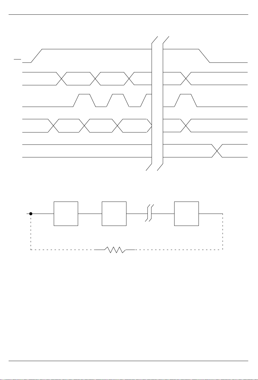
Information is written to and read from the wiper 0 and
wiper 1 registers and the stack select bit via the 17-bit
I/O shift register. The I/O shift register is serially loaded
by a 3 wire serial port consisting of RST
, DQ, and CLK. It
is updated by transferring all 17 bits (Figure 2). Data can
be entered into the 17 bit shift register only when the
input is at a high level. While at a high level, the
RST
RST function allows serial entry of data via the D/Q pin.
The potentiometers always maintain their previous value until RST is taken to a low level, which terminates
data transfer. While RST input is low, the DQ and CLK
inputs are ignored.
Valid data is entered into the I/O shift register while RST
is high on the low-to-high transition of the CLK input.
Data input on the DQ pin can be changed while the clock
input is high or low, but only data meeting the setup requirements will enter the shift register. Data is always
entered starting with the value of the stack select bit.
The next 8 bits to be entered are those specifying the
wiper 1 setting. The MSB of these 8 bits is sent first. The
next 8 bits to be entered are those specifying the wiper 0
setting, sent MSB first. The 17th bit to be entered, therefore, will be the least significant bit of the wiper 0 setting.
If fewer than 17 bits are entered, the value of the potentiometer settings will result from the number of bits that
were entered plus the remaining bits of the old value
shifted over by the number of bits sent. If more than 17
bits are sent, only the last 17 bits are left in the shift register. Therefore, sending other than 17 bits can produce
indeterminate potentiometer settings.
As bits are entered into the shift register, the previous
value is shifted out bit by bit on the cascade serial port
pin (COUT). By connecting the COUT pin to the DQ pin
of a second DS1667, multiple devices can be daisy
chained together as shown in Figure 3.
When connecting multiple devices, the total number of
bits sent is always 17 times the number of DS1667s in
the daisy chain. In applications where it is desirable to
read the settings of potentiometers, the COUT pin of the
last device connected in a daisy chain must be connected back to the DQ input of the first device through a
resistor with a value of 1K to 10K. This resistor provides
isolation between COUT and DQ when writing to the device (see Figure 3).
When reading data, the DQ line is left floating by the
reading device. When RST
is held low, bit 17 is always
present on the COUT pin, which is fed back to the input
DQ pin through the resistor (see Figure 4).This data bit
can now be read by the reading device. The RST
pin is
then transitioned high to initiate a data transfer. When
the CLK input transitions low to high, bit 17 is loaded into
the first position of the I/O shift register and bit 16 becomes present on COUT and DQ. After 17 bits (or 17
times the number of devices for a daisy chain), the data
has shifted completely around and back to its original
position. When RST
is transitioned back low to end data
transfer, the value (the same as before the read occurred) is loaded into the wiper 0 and wiper 1 registers
and the stack select bit.
When power is applied to the DS1667, the device always has the wiper settings at half position and the
stack select bit is at zero.
021492 3/11
Page 4
DS1667
WRITING DATA Figure 2
RST
DQ
CLK
PREVIOUS
I/O SR
WIPER 0 & 1
STACK SELECT
CONTROL
REG.
PREVIOUS VALUE
CASCADING MULTIPLE DEVICES Figure 3
DQ DQ DQ
DS1667
#1
C
OUT
DS1667
#2
DON’T CAREDON’T CARE BIT 16 BIT 15 BIT 14 BIT 0
NEW CONTROL REG.+0, 1+0
NEW VALUE
C
DS1667
C
OUT
#3
OUT
021492 4/11
OPTIONAL FEEDBACK
RESISTOR FOR READING DATA
Page 5

READING DATA Figure 4
RST
DS1667
C
OUT
CLK
CONTROL
REGISTERS
BIT 16
BIT 15 BIT 14 BIT 0 BIT 16
CURRENT SETTINGS
DS1667 LINEARITY MEASUREMENTS
An important specification for the DS1667 is linearity,
that is, for a given digital input, how close the analog output is to that which is expected.
The test circuit used to measure the linearity of the
DS1667 is shown in Figure 5. Note that to get an accurate output voltage it is necessary to assure that the output current is 0, in order to negate the effects of wiper
impedance RW which is typically 400 ohms. For any
given setting N for the pot, the expected voltage output
at SOUT is:
VO = -5 + [10 X (N/256)] (in volts)
Absolute linearity is a comparison of the actual measured output voltage versus the expected value given
by the equation above, and is given in terms of an LSB,
which is the change in expected output when the digital
input is incremented by 1. In this case the LSB is 10/256
or 0.03906 volts. The equation for the absolute linearity
of the DS1667 is:
(actual) VO(expected)
V
O
LSB
The specification for absolute linearity of the DS1667 is
+
1 LSB typical.
Relative linearity is a comparison of the difference of actual output voltages of two successive taps and the difference of the expected output voltages of two successive taps. The expected difference of output voltages is
1 LSB or 0.03906V for the measurement system of Fig-
AL (in LSBs)
NO
CHANGES
ure 5. Relative linearity is expressed in terms of an LSB
and is given by the equation:
(actual) LSB
V
O
LSB
RL
The specification for relative linerity of the DS1667 is
+
0.5 LSB typical.
Figure 6 is a plot of absolute linearity (AL) and relative
linearity (RL) versus wiper setting for a typical DS1667
at 25°C.
DESCRIPTION AND OPERATION - OP AMP
SECTION
The DS1667 contains two operational amplifiers which
are ideal for operation from a single 5V supply and
ground or from +5V supplies (see Figure 1). An internal
resistor divider defines the internal reference of the op
amp to be halfway between the power supplies, i.e.:
V
V
DD
B
2
For optimal performance, choose analog ground to be
this value. The operational amplifiers feature rail to rail
output swing in addition to an input common mode
range that includes the positive rail. Performance features include broad band noise immunity as well as voltage gain into realistic loads specified at both 600 ohms
and 2K ohms. High voltage gain is produced with low
input offset voltage and low offset voltage drift. Current
consumption is less than 1.9 mA per amplifier and the
device is virtually immune to latchup.
021492 5/11
Page 6

DS1667
LINEARITY MEASUREMENT CONFIGURATION Figure 5
+5V
HX
X=0 POT0
X=1 POT1
POTX
RWX
LX
–5V
WX
DS1667 ABSOLUTE AND RELATIVE LINEARITY Figure 6
I0 = 0
+
V
0
–
021492 6/11
Page 7
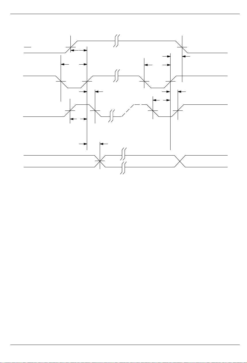
TIMING DIAGRAM: RESISTOR SECTION Figure 7
DS1667
RST
CLK
DQ INPUTS
C
OUT
t
HHT
t
W
t
H
t
SU
t
PLH
t
HLT
t
W
t
H
t
SU
021492 7/11
Page 8
DS1667
ABSOLUTE MAXIMUM RATINGS*
Voltage on Any Pin Relative to Ground (VB = GND) –0.5V to +7.0V
Voltage on Resistor Pins when V
Voltage on V
Operating Temperature 0°C to 70°C
B
Storage Temperature –55°C to +125°C
Soldering Temperature 260°C for 10 seconds
*This is a stress rating only and functional operation of the device at these or any other conditions above those
indicated in the operation sections of this specification is not implied. Exposure to absolute maximum rating
conditions for extended periods of time may affect reliability.
= -5.5V -5.5V to +7.0V
B
-5.5V to GND
RECOMMENDED DC OPERATING CONDITIONS RESISTOR SECTION (0°C to 70°C)
PARAMETER SYMBOL MIN TYP MAX UNITS NOTES
Positive Supply Voltage V
Input Logic 1 V
Input Logic 0 V
Negative Supply Voltage V
CC
IH
IL
B
+4.5 5.0 5.5 V 1
2.0 VCC+0.5 V 1
-0.5 +0.8 V 1
-5.5 GND V 1
Resistor Inputs L, H, W VB - 0.5 VCC + 0.5 V 2
DC ELECTRICAL CHARACTERISTICS
RESISTOR SECTION (0
°C to 70°C; V
PARAMETER SYMBOL MIN TYP MAX UNITS NOTES
Positive Supply Current I
Negative Supply Current I
Input Leakage I
Wiper Resistance R
Wiper Current I
Output Leakage I
Logic 1 Output @ 2.4 Volts I
Logic 0 Output @ 0.4 Volts I
End–to–End Resistor Tolerance TOL
CC
W
LO
OH
OL
B
U
W
–1 +1 µA
400 1000 ohms
–1 +1 µA
–1.0 mA
R
–20 +20 %
Noise (ref: 1V) N –120
Absolute Linearity AL 1.0 LSB
Relative Linearity RL 0.5 LSB
Resistor Temperature Coefficient TC
R
= 5.0V ± 10%, VB = -5.0V ± 10%)
CC
3 5 mA
3 5 mA
1 mA
4 mA
dB
Hz
850 ppm
°C
021492 8/11
Page 9
DS1667
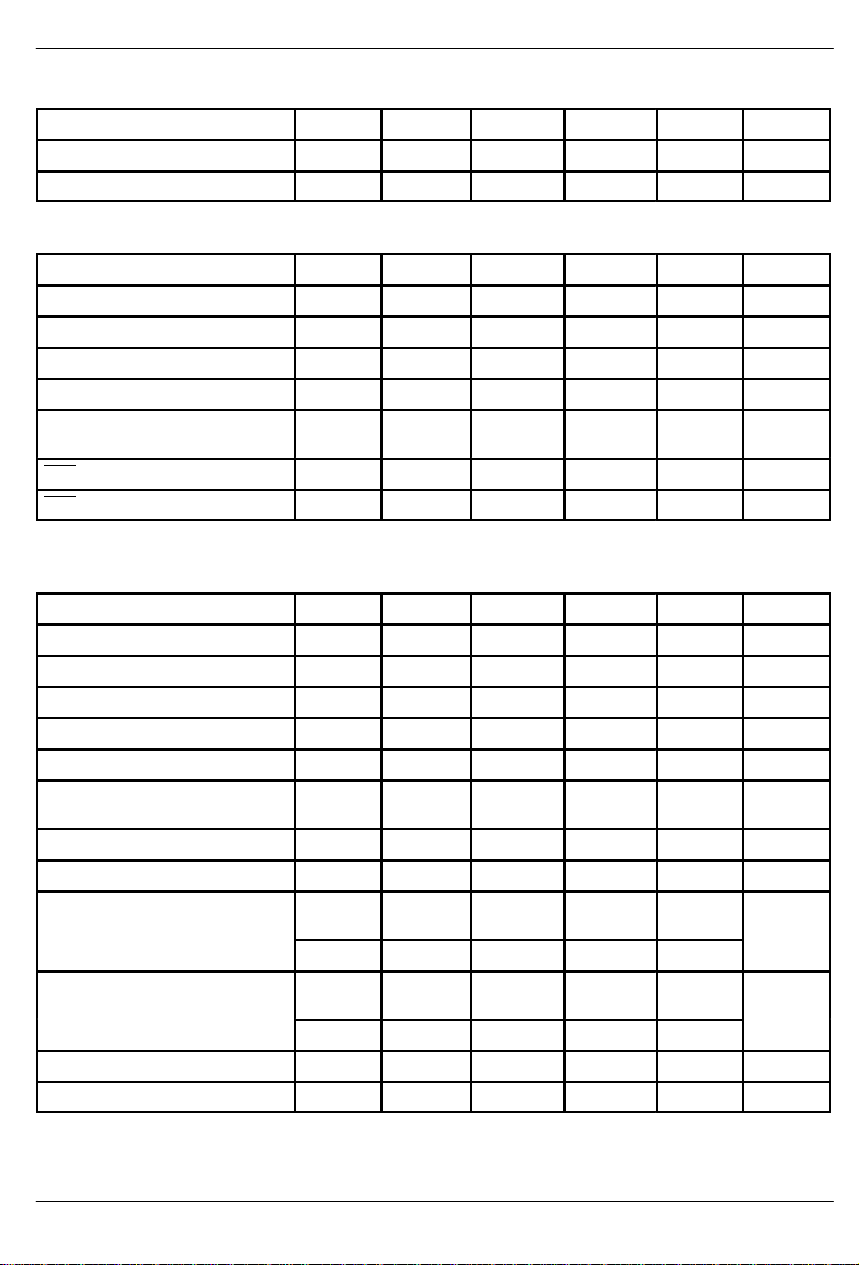
CAPACITANCE (tA = 25°C)
PARAMETER SYMBOL MIN TYP MAX UNITS NOTES
Input Capacitance C
Output Capacitance C
IN
OUT
5 pF
7 pF
AC ELECTRICAL CHARACTERISTICS RESISTOR SECTION (0°C to 70°C, VCC = 5V ± 10%)
PARAMETER SYMBOL MIN TYP MAX UNITS NOTES
CLK Frequency f
Width of CLK Pulse t
Data Setup Time t
Data Hold Time t
Propagation Delay Time Low to
High Level Clock to Output
RST High to Clock Input High t
RST Low from Clock Input High t
CLK
SU
t
PLH
HHT
HLT
W
50 ns
30 ns
H
10 ns
50 ns
50 ns
10 MHz
50 ns 3
OPERATIONAL AMPLIFIER SECTION
DC ELECTRICAL CHARACTERISTICS (0
°C to 70°C; V
PARAMETER SYMBOL MIN TYP MAX UNITS NOTES
Input Offset Voltage V
Input Offset Voltage Drift V
Common Mode Rejection CM
Positive Power Supply Rejection +PS
Negative Power Supply Rejection –PS
Input Common Mode Voltage
Range
C
OS
OSD
CCM
R
R
R
VB+1.5V V
Large Signal Voltage Gain 106 dB RL=2KΩ
Large Signal Voltage Gain 96 dB
Output Swing V
Output Swing V
Output Swing V
Output Swing V
Output Current
V
Output Current V
SWGH
SWGL
SWGH
SWGL
O,SOURCE
O,SINK
4.6 4.7 V R
–4.7 –4.6 V V
4.5 4.6 V R
–4.6 –4.5 V V
13 58 mA
13 63 mA VO = +5V
= 5.0V ± 10%, VB = -5.0V ± 10%)
CC
5 10 mV
10 uV/°C
62 dB
62 dB
62 dB
CC
V
RL=600KΩ
=2KΩ
L
to GND
= –5V
B
=600KΩ
L
to GND
= –5V
B
VO = 0V
021492 9/11
Page 10

DS1667
OPERATIONAL AMPLIFIER SECTION
AC ELECTRICAL CHARACTERISTICS (0
°C to 70°C; V
PARAMETER SYMBOL MIN TYP MAX UNITS NOTES
Slew Rate V
SL
0.7 2 V/µs 6
Gain Bandwidth Product GBP 2.5 MHz 5
Phase Margin PM 75 deg 5
Gain Margin GM 20 dB 5
Amp–to–Amp Isolation AAI 130 dB
Input Referred Voltage Noise IRVF 100
Input Referred Current Noise IRV1 .0002
Total Harmonic Distortion HD 0.1 % F=10 KHz
= 5.0V ± 10%)
CC
Ǹ
nVń Hz
Ǹ
pAń Hz
F=1 KHz
F=1 KHz
AV=–10
RL=2KΩ
=1V
V
O
NOTES:
1. All voltages are referenced to ground.
2. Resistor inputs cannot exceed the substrate bias voltage in the negative direction
3. Measured with a load as shown in Figure 8.
4. Over a frequency range of 0 - 1 KHz.
5. Load is R
6. VDD = +5.0V VB = -5.0V connected as voltage follower with 10V step input and RL = ∞.
7. To achieve best op amp performance, V
ground =
= 600 Ω CL = 10 pF
L
.
) V
V
DD
B
2
= +5.0V VB = -5.0V and analog ground = 0V . In general analog
DD
PP
8. OP AMPS idle, no load.
021492 10/11
Page 11

DS1667
LOAD SCHEMATIC Figure 8
D.U.T.
680 Ω
+5 VOLTS
1.1K
50 pF
021492 11/11
 Loading...