Page 1

r
www.dalsemi.com
DS1666
Audio Digital Resisto
FEATURES
128 position, digitally controlled poten-
tiometer
Operates from a +5 volts power supply with
TTL signal inputs
Wide analog voltage range of ±5 volts
Low-power CMOS
14-pin DIP or 16-pin SOIC for surface
mount applications
Default position on power up sets wiper
position to 10% of active digital taps (3% of
the total end-to-end resistance)
Operating temperature range
– Industrial temp. range: -40°C to +85°C
Resistance/Step
Resistance values Low End High End -3dB Point
DS1666-10 10K 24ȍ 152ȍ 1.0 MHz
DS1666-50 50K 122ȍ 759ȍ 200 kHz
DS1666-100 100K 243ȍ 1.519ȍ 100 kHz
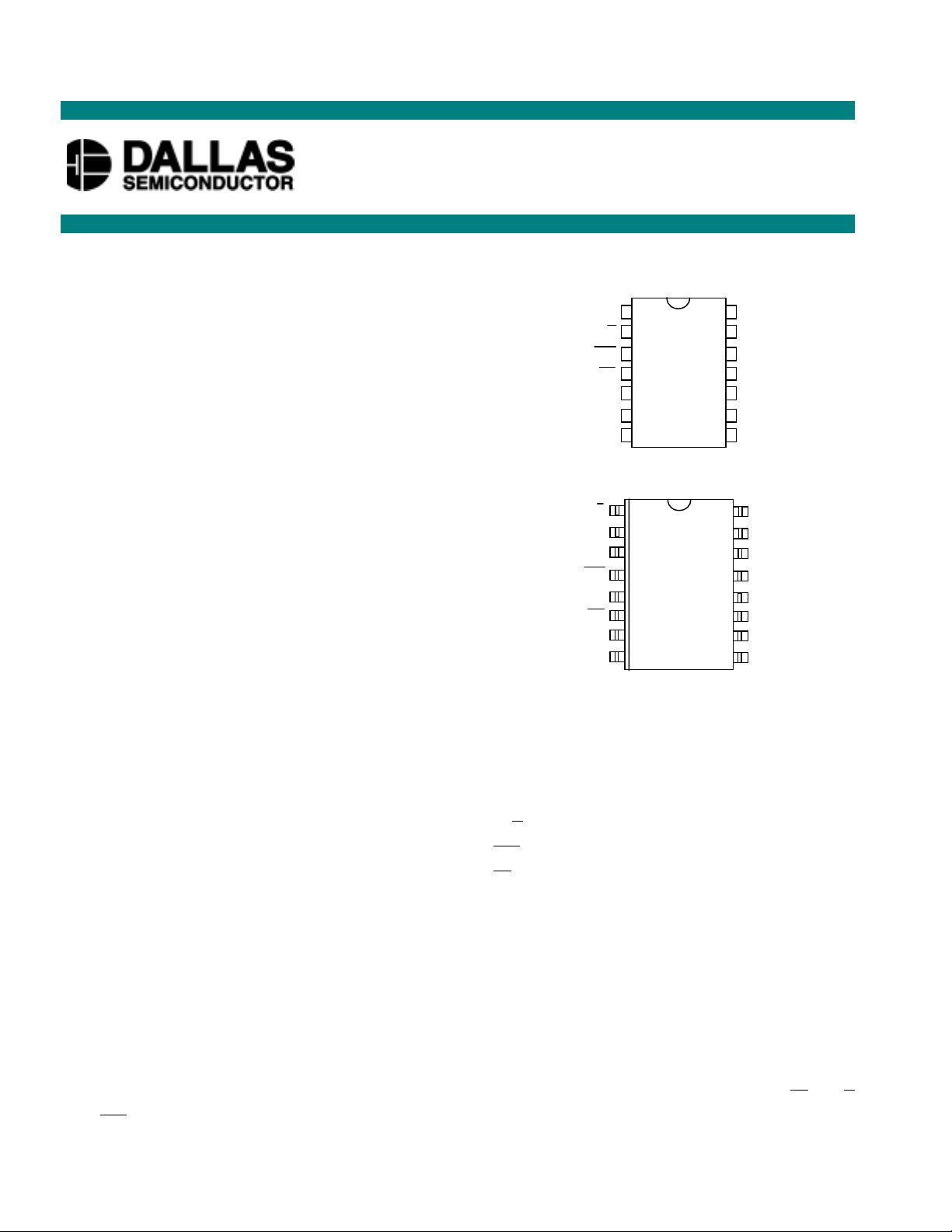
PIN ASSIGNMENT
1
NC
2
U/D
3
INC
4
CS
GND
See Mech. Drawings Section
U/D
NC
NC
INC
NC
CS
NC
GND
See Mech. Drawings Section
5
6
NC
7
NC
14-PIN DIP (300 MIL)
1
2
3
4
5
6
7
8
16-PIN SOIC (300 MIL)
14
13
12
11
10
16
15
14
13
12
11
10
NC
V
CC
V
B
V
W
V
H
9
V
L
8
NC
V
CC
NC
V
B
V
W
V
H
NC
NC
9
V
L
PIN DESCRIPTIONS
V
H
V
L
V
W
U/ D - Up/Down Control
INC - Wiper Movement Control
CS - Chip Select for Wiper Movement
NC - No Connection
V
CC
GND - Ground
V
B
- High Terminal of Potentiometer
- Low Terminal of Potentiometer
- Wiper Terminal of Potentiometer
- 5V Power Supply Input
- Substrate Bias Voltage (0 to -5V)
DESCRIPTION
The DS1666 Audio Digital Resistor is a solid-state potentiometer composed of 127 digitally controlled
resistive elements. Between each resistive section and both ends of the potentiometer are tap points
multiplexed to the wiper. The position of the wiper on the resistance array is controlled by the CS , U/ D
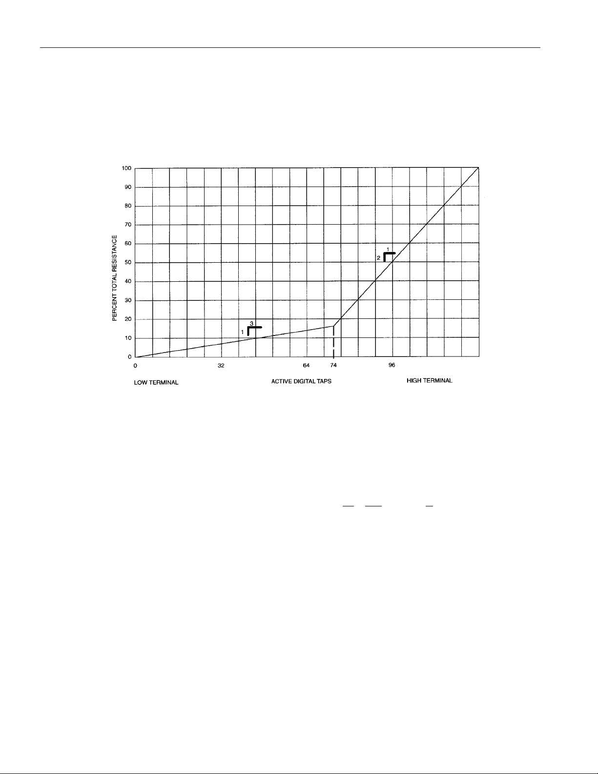
and INC inputs. The taper of the DS1666 is shown in Figure 1.
1 of 9 102899
Page 2

DS1666
The DS1666 is uniquely designed to provide a potentiometer that is pseudo-logarithmic rather than linear
across its entire range. The lower half of the potentiometer advances 1% of total resistance for each 3%
of scale advanced, providing for precise amplification of low volume signals. The upper half of the
potentiometer advances 2% of resistance for every 1% of scale advanced, providing for the lower
resolution gain required for high volume amplification.
GRAPH OF AUDIO TAPER Figure 1
OPERATION
The DS1666 has a total of 128 tap-points including the VL and VH terminals. A total of 127 resistive
segments exist between the VL and VH terminals. These tap-points are accessible to the VWterminal
whose position is controlled via a 3-terminal control port. A block diagram of the DS1666 is shown in
Figure 2.
The 3-terminal port of the DS1666 provides an increment/ decrement interface which is activated via a
chip select input. This interface consists of the input signals CS , INC , and U/ D . These input signals
control a 7-bit up/down counter. The output of the 7-bit up/down counter controls a 1 of 128 decoder to
select wiper position. The timing diagram for the 3-terminal interface control is shown in Figure 4.
ANALOG CHARACTERISTICS
The DS1666 has a pseudo-logarithmic resistor array that resembles an audio taper potentiometer as
shown in Figure 1. Taps on the lower portion of the potentiometer increment 0.25% of the total
resistance and are specified to within ±0.5% of the expected value. Taps on the higher portion increment
1.5% of the total resistance and are specified to within ±2.0% of the expected value.
End-to-End Resistance Tolerance = ±20 %
Temperature Coefficient = 750 PPM/°C typical
2 of 9 102899
Page 3

DS1666
PIN DESCRIPTIONS
VCC - Power Supply. The DS1666 will support supply voltages ranging from +4.5 to +5.5 volts.
GND - Ground Terminal.
VB- Negative Bias. The DS1666 will support a negative bias ranging from 0 to -5 volts.
H - High-Terminal of Potentiometer. It is not required that this terminal be connected to a potential
greater than the V
voltage, (V
), or go below the negative bias, (VB).
CC
VL - Low-Terminal of Potentiometer. It is not required that this terminal be connected to a potential less
than the V
terminal. Voltage applied to the VLterminal cannot exceed the power-supply voltage, (VCC),
H
or go below the negative bias (VB).
V
- Wiper of the Potentiometer. Its position on the resistor array is controlled by the 3-terminal control
W
port. Voltage applied to the wiper cannot exceed the power-supply voltage, VCC, or go below the
negative bias (VB).
CS - Chip Select. The CS input is used to activate the control port of the DS1666. This input is active
low. When in a high-state, activity on the INC and U/ D port pins will not affect or change wiper
position.
terminal. Voltage applied to the VHterminal can not exceed the power-supply
L
INC - Wiper Movement Control. This input provides for wiper position changes when the CS pin is low.
Wiper position changes will occur one position per high-to-low transition of this input signal. Position
changes will not occur if the CS pin is in a high-state.
U/ D - Up/Down Control. This input sets the direction of wiper movement. When in a high-state and CS
is low, any high-to-low transition on INC will cause a one position movement of the wiper towards the
VH terminal. When in a low-state and CS is low, any high-to-low transitions on INC will cause the
position of the wiper to move towards the VL terminal.
3 of 9 102899
Page 4

BLOCK DIAGRAM Figure 2
DS1666
MODE SELECTION Figure 3
4 of 9 102899
Page 5

DS1666
ABSOLUTE MAXIMUM RATINGS*
Voltage on CS , INC , U/ D and U/ D and VCC Relative to Ground -0.5V to +7.0V
Voltage on VH, VL and VW Relative to Ground -6.5V to +6.5V
Voltage on V
B
-6.5V to GND
Operating Temperature -40° to +85°C
Storage Temperature -55°C to +125°C
Soldering Temperature 260°C for 10 seconds
* This is a stress rating only and functional operation of the device at these or any other conditions above
those indicated in the operation sections of this specification is not implied. Exposure to absolute
maximum rating conditions for extended periods of time may affect reliability.
RECOMMENDED DC OPERATING CONDITIONS (-40°C to +85°C)
PARAMETER SYMBOL MIN TYP MAX UNITS NOTES
Supply Voltage V
Input Logic 1 V
Input Logic 0 V
VH, VL, VW Voltage V
VB Voltage V
CC
IH
IL
R
B
+4.5 5.0 5.5 V 1
2.0 VCC+0.5 V 1
-0.5 +0.8 V 1
VB-0.3 VCC+0.3 V 1, 3
-5.5 GND V 1
DC ELECTRICAL CHARACTERISTICS (-40°C to +85°C; VCC = 5.0V ± 10%)
PARAMETER SYMBOL MIN TYP MAX UNITS NOTES
Supply Current I
Input Leakage I
Wiper Resistance R
Wiper Current I
CC
LI
W
-1 +1 µA
W
0.2 4.5 mA 4
350 900
Ω
1mA
2
CAPACITANCE (tA=25°C)
PARAMETER SYMBOL CONDITION TYP MAX UNITS NOTES
Capacitance C
IN
tA=25°C
6pF
5 of 9 102899
Page 6

DS1666
ANALOG RESISTOR CHARACTERISTICS (-40°C to +85°C; VCC = 5.0V ± 10%)
PARAMETER SYMBOL MIN TYP MAX UNITS NOTES
Total Resistance
“-10”
“-50”
“-100”
10
50
100
KΩ
KΩ
KΩ
5
5
5
End-to-End Resistor Tolerance -20 +20 % 8
Absolute Tolerance
Low End (0.25% Increments)
High End (1.5% Increments)
-3 dB Cutoff Frequency f
CUTOFF
Temperature Coefficient 750
-0.5
-2.0
+0.5
+2.0
%
%
MHz 7
ppm/°C
6
6
AC ELECTRICAL CHARACTERISTICS (-40°C to +85°C; VCC = 5.0V ± 10%)
PARAMETER SYMBOL MIN TYP MAX UNITS NOTES
CS to INC Setup
INC High to U/ D Change
t
CI
t
ID
100 ns
100 ns
U/ D to INC Setup
INC Low Period
INC High Period
INC Low to Wiper Change
t
DI
t
IL
t
IH
t
IW
1µs
500 ns
1µs
200 ns
6 of 9 102899
Page 7

AC TIMING Figure 4
NOTES:
1. All Voltages are referenced to ground.
DS1666
2. Typical Values are for TA=25°C and nominal supply voltages.
3. Resistors input voltages cannot go below VB or exceed VCC by the amounts shown.
4. Maximum current specifications are based on the clock rate of INC input. This specification
represents the current required when changing the wiper position.
5. The DS1666 is available in three end-to-end resistor values. These include 10KΩ for the DS1666-10;
50KΩ for the DS1666-50; and 100KΩ for the DS1666-100.
6. Absolute tolerance is used to compare measured wiper voltage versus expected wiper voltage as
determined by wiper position.
7. -3dB cutoff frequency characteristics for the DS1666 depend on potentiometer total resistance. The
DS1666-10 is 1 MHz; the DS1666-50 is 200 KHz; and the DS1666-100 is 100 KHz.
8. Valid at 25°C only
AC TEST CONDITIONS
Input Pulse Levels 0V to 3V
Input Rise and Fall Times 10 ns
7 of 9 102899
Page 8

DS1666 ORDERING INFORMATION
ORDERING
NUMBER
DS1666-010 14L DIP -40°C TO +85°C
PACKAGE OPERATING
TEMPERATURE
DS1666
VERSION
10 kΩ
DS1666-050 14L DIP -40°C TO +85°C
DS1666-100 14L DIP -40°C TO +85°C
DS1666S-010* 16L SOIC (300-mil) -40°C TO +85°C
DS1666S-050* 16L SOIC (300-mil) -40°C TO +85°C
DS1666S-100* 16L SOIC (300-mil) -40°C TO +85°C
* Add “/T & R” for tape and reel packaging.
50 kΩ
100 kΩ
10 kΩ
50 kΩ
100 kΩ
8 of 9 102899
Page 9

DS1666
DATA SHEET REVISION SUMMARY
The following represent the key differences between 07/26/93 and 06/18/97 version of the DS1666 data
sheet. Please review this summary carefully.
1. Remove commercial temp grade reference.
2. Add order info table.
3. Improve operating description and add “ANALOG Resistor CHARACTERISTICS”.
9 of 9 102899
 Loading...