

Page 1
www.dalsemi.com
A8A9A
A
A12A
A
A
A
A
A
A
A
A
A
A1A
DS1643/DS1643P
Nonvolatile Timekeeping RAM
FEATURES
Integrated NV SRAM, real time clock,
crystal, power-fail control circuit and lithium
energy source
Clock registers are accessed ident ically to the
static RAM. These registers are resident in the
eight top RAM locations.
Totally nonvolatile with over 10 years of
operation in the absence of power
Access times of 70 ns and 100 ns
BCD coded year, month, date, day, hours,
minutes, and seconds with leap year
compensation valid up to 2100
Power-fail write protection allows for ±10%
VCC power supply tolerance
Lithium energy source is electrically
disconnected to retain freshness until power is
applied for the first time
DS1643 only (DIP Module)
– Standard JEDEC byte-wide 8K x 8 RAM
pinout
DS1643P only (PowerCap Module Board)
– Surface mountable package for direct
connection to PowerCap containing
battery and crystal
– Replaceable battery (PowerCap)
– Power-fail output
– Pin-for-pin compatible with other
densities of DS164XP Timekeeping RAM
ORDERING INFORMATION
DS1643-XXX 28-pin DIP module
-70 70 ns access
-100 100 ns access
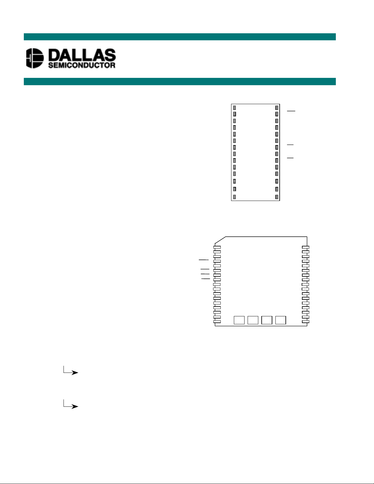
PIN ASSIGNMENT
1
NC
A12
DQ0
DQ1
DQ2
GND
28-PIN Encapsulated Package
NC
NC
NC
PFO
V
CC
WE
OE
CE
DQ7
DQ6
DQ5
DQ4
DQ3
DQ2
DQ1
DQ0
GND
34-PIN PowerCap Module Board
(USES DS9034PCX PowerCap)
2
A7
3
4
A6
A5
5
6
A4
A3
7
A2
8
A1
9
A0
10
11
12
13
14
(700-mil Extended)
1
2
3
4
5
6
7
8
9
10
11
12
13
14
15
X1 GND
16
17
VCC
28
27
CE2
26
25
24
23
22
21
20
19
18
17
16
15
V
BAT
X2
11
OE
10
CE
DQ7
DQ6
DQ5
DQ4
DQ3
34
33
32
31
30
29
28
27
26
25
24
23
22
21
20
19
18
NC
NC
NC
NC
11
10
9
8
7
6
5
4
3
2
0
*DS1643P-XXX 34-pin PowerCap Module Board
-70 70 ns access
-100 100 ns access
*DS9034PCX PowerCap
(Required; must be ordered
separately)
1 of 14 022101
Page 2

DS1643/DS1643P
PIN DESCRIPTION
A0-A12 - Address Input
CE - Chip Enable
CE2 - Chip Enable 2 (DIP Module
only)
OE - Output Enable
WE - Write Enable
V
- +5 Volts
CC
GND - Ground
DQ0-DQ7 - Data Input/Output
NC - No Connect
RST - Power-on Reset Output
(PowerCap Module board only)
X1, X2 - Crystal Connection
V
- Battery Connection
BAT
DESCRIPTION
The DS1643 is a 8K x 8 nonvolatile static RAM with a full function Real Time Clock (RTC) which are
both accessible in a byte-wide format. The nonvolatile timekeeping RAM is functionally equivalent to
any JEDEC standard 8K x 8 SRAM. The device can also be easily substituted in ROM, EPROM and
EEPROM sockets providing read/write nonvolatility and the addition of the real time clock function. The
real time clock information resides in the eight uppermost RAM locations. The RTC registers contain
year, month, date, day, hours, minutes, and seconds data in 24-hour BCD format. Corrections for the d ay
of the month and leap year are made automatically. The RTC clock registers are double-buffered to avoid
access of incorrect data that can occur during clock update cycles. The double-buffered system also
prevents time loss as the timekeeping countdown continues unabated by access to time register data. The
DS1643 also contains its own power-fail circuitry which deselects the device when the V
an out of tolerance condition. This feature prevents loss of data from unpredictable system operation
brought on by low V
as errant access and update cycles are avoided.
CC
supply is in
CC
PACKAGES
The DS1643 is available in two packages: 28-pin DIP module and 34-pin PowerCap module. The 28-pin
DIP style module integrates the crystal, lithium energy source, and silicon all in one package. The 34-pin
PowerCap Module Board is designed with contacts for connection to a separate PowerC ap (DS9034PCX)
that contains the crystal and battery. This design allows the PowerCap to be mounted on top of the
DS1643P after the completion of the surface mount process. Mounting the PowerCap aft er the surface
mount process prevents damage to the crystal and battery due to high temperatures required for solder
reflow. The PowerCap is keyed to prevent reverse insertion. The PowerCap Module Board and PowerCap
are ordered separately and shipped in separate containers. The part number for the PowerCap is
DS9034PCX.
CLOCK OPERATIONS-READING THE CLOCK
While the double-buffered register structure reduces the chanc e of r eadin g incor rect d ata, internal updates
to the DS1643 clock registers should be halted before clock data is read to prevent reading of data in
transition. However, halting the internal clock register updating process does not affect clock accuracy.
Updating is halted when a one is written into the read bit, the seventh most significant bit in the control
register. As long as a 1 remains in that position, updating is halted. After a halt is issued, the registers
reflect the count, that is day, date, and time that was current at the moment the halt command was issued.
However, the internal clock registers of the double-buffered s ystem continue to update so that the clock
accuracy is not affected by the access of data. All of the DS1643 registers are updated simultaneously
after the clock status is reset. Updating is within a second after the read bit is written to 0.
2 of 14
Page 3
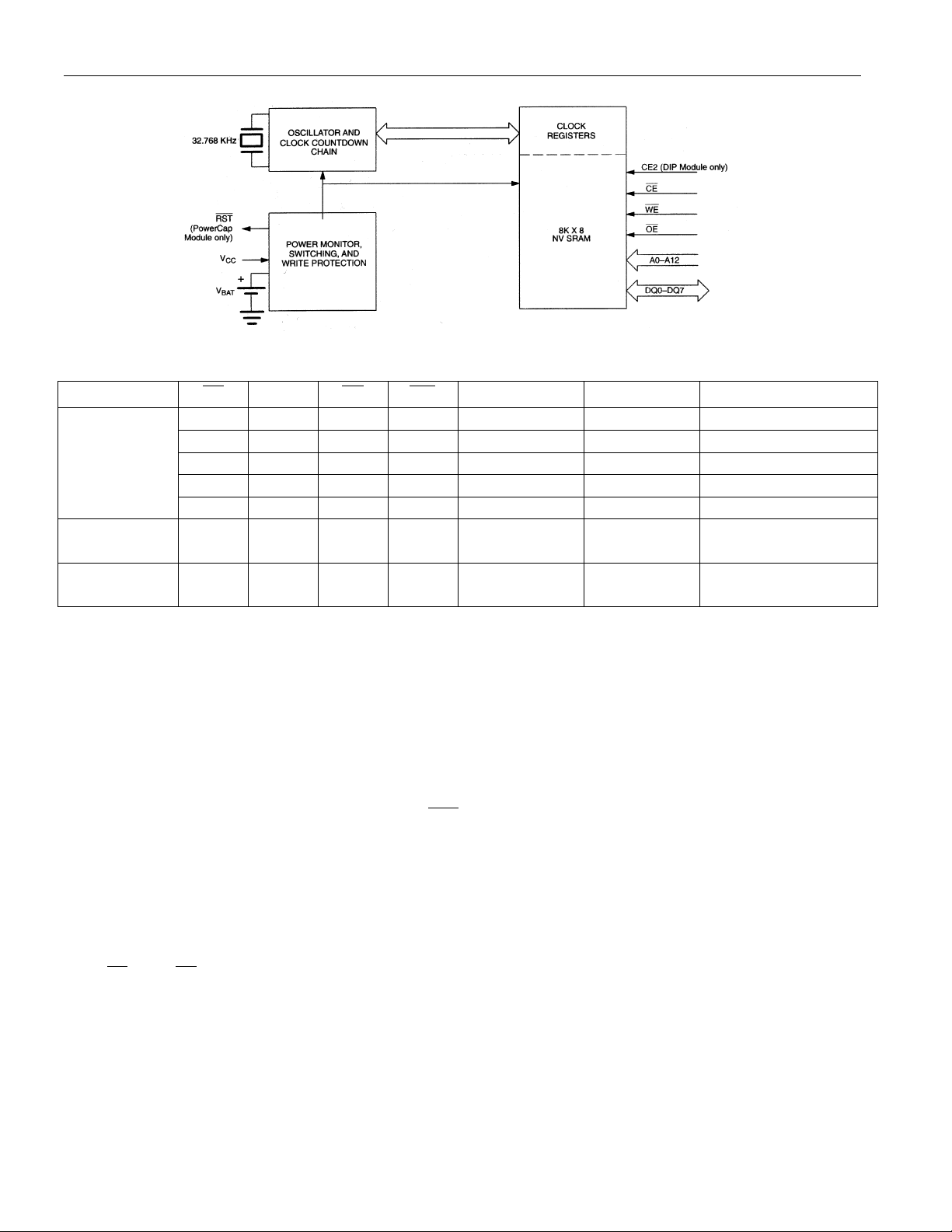
BLOCK DIAGRAM DS1643 Figure 1
DS1643 TRUTH TABLE Table 1
V
CC
5 VOLTS
± 10%
<4.5 VOLTS
>V
BAT
<V
BAT
CE
V
IH
XVILX X DESELECT H IGH Z STANDBY
V
IL
V
IL
V
IL
XXXXDESELECTHIGH ZCMOS STANDBY
XXXXDESELECTHIGH ZDATA RETENTION
CE2
OE WE
X X X DESELECT HIGH Z STANDBY
V
V
V
IH
IH
IH
XVILWRITE DATA IN ACTIVE
V
V
IL
IH
V
V
IH
IH
DS1643/DS1643P
MODE DQ POWER
READ DATA OUT ACTIVE
READ HIGH Z ACTIVE
MODE
SETTING THE CLOCK
The 8-bit of the control register is the write bit. Setting the write bit to a 1, like the read bit, halts updates
to the DS1643 registers. The user can then load them with the correct day, date and time data in 24 hour
BCD format. Resetting the write bit to a 0 then transfers those values to the actual clock counters and
allows normal operation to resume.
STOPPING AND STARTING THE CLOCK OSCILLATOR
The clock oscillator may be stopped at any time. To increase the shelf life, the oscillator can be turned off
to minimize current drain from the battery. The
OSC bit is the MSB for the seconds registers. Setting it to
a 1 stops the oscillator.
FREQUENCY TEST BIT
Bit 6 of the day byte is the frequency test bit. When the frequency test bit is set to logic 1 and the
oscillator is running, the LSB of the seconds register will toggle at 512 Hz. When the seconds register is
being read, the DQ0 line will toggle at the 512 Hz frequency as long as conditions for access remain valid
(i.e., CE low, OE low, CE2 high, and address for seconds register remain valid and stable).
CLOCK ACCURACY (DIP MODULE)
The DS1643 is guaranteed to keep time accuracy to within ±1 minute per month at 25°C.
CLOCK ACCURACY (POWERCAP MODULE)
The DS1643P and DS9034PCX are each individually tested for accuracy. Once mounted together, the
module is guaranteed to keep time accuracy to within ±1.53 minutes per month (35 ppm) at 25°C.
3 of 14
Page 4
DS1643/DS1643P
DS1643 REGISTER MAP - BANK1 Table 2
ADDRES
S
B
7
B
6
B
5
1FFF - - - - - - - - YEAR 00-99
1FFE X X X - - - - - MONTH 01-12
1FFDXX------ DATE01-31
1FFC X FT X X X - - - DAY 01-07
1FFB X X - - - - - - HOUR 00-23
1FFAX-------MINUTES00-59
1FF9
OSC
-------
1FF8 WRXXXXXXCONTROLA
OSC = STOP BIT
W = WRITE BIT X = UNUSED
DATA
B
4
B
3
B
2
B
1
B
0
FUNCTION
SECONDS 00-59
R = READ BIT FT = FREQUENCY TEST
NOTE:
All indicated “X” bits are not dedicated to any particular function and can be used as normal RAM bits.
RETRIEVING DATA FROM RAM OR CLOCK
The DS1643 is in the read mode whenever WE (write enable) is high and CE (chip enable) is low. The
device architecture allows ripple-through access to any of the address locat ions in the NV SRAM. Valid
data will be available at the DQ pins within t
and OE access times and states are satisfied. If CE or OE access times are not met, valid data will be
available at the latter of chip enable access (t
data input/output pins (DQ) is controlled by CE and OE . If the outputs are activated before t
lines are driven to an intermediate state until tAA. If the address inputs are changed while CE and OE
remain valid, output data will remain valid for output data hold time (tOH) but will then go indeterminate
until the next address access.
after the last address input is stable, providing that the CE
AA
) or at output enable access time (t
CEA
). The state of the
OEA
, the d ata
AA
WRITING DATA TO RAM OR CLOCK
The DS1643 is in the write mode whenever WE and CE are in their active st ate. The start of a write is
referenced to the latter occurring transition of WE or CE . The addresses must be held valid throu ghout
the cycle.
write cycle. Data in must be valid t
typical application, the
CE or WE must return inactive for a minimum of t
prior to the end of write and remain valid for tDH afterward. In a
DS
OE signal will be high during a write cycle. However, OE can be active provided
that care is taken with the data bus to avoid bus contention. If
prior to the initiation of another read or
WR
OE is low prior to WE transitioning low
the data bus can become active with read data defined by the addr ess inputs. A low transition on WE will
then disable the outputs t
after WE goes active.
WEZ
DATA RETENTION MODE
When VCC is within nominal limits (VCC > 4.5 volts) the DS1643 can be accessed as described above with
read or write cycles. However, when V
protection occurs) the internal clock registers and RAM are blocked from access. This is accomplished
internally by inhibiting access via the CE signal. At this time the power-on reset output signal (RST ) will
be driven active low and will remain active until V
level of the internal battery supply, power input is switched from the V
clock activity, RAM, and clock data are maintained from the battery until V
is below the power-fail point VPF (point at which write
CC
returns to nominal levels. When VCC falls below the
CC
pin to the internal battery and
CC
is returned to nominal
CC
4 of 14
Page 5

DS1643/DS1643P
level. The RST signal is an open drain output and requires a pull up. Except for the RST , all control, data,
and address signals must be powered down when VCC is powered down.
BATTERY LONGEVITY
The DS1643 has a lithium power source that is designed to provide energy for clock activity, and clock
and RAM data retention when the V
is sufficient to power the DS1643 continuously for the life of the equipment in which it is installed. For
specification purposes, the life expectanc y is 10 years at 25°C with the internal clock os cillator running in
the absence of V
power. Each DS1643 is shipped from Dallas Semiconducto r with its lithium energy
CC
source disconnected, guaranteein g full energy capacit y. When VCC is first applied at a level greater than
VPF, the lithium energy source is enabled for battery backup operation. Actual life expectancy of the
Ds1643 will be much longer than 10 years since no lithium battery energy is consumed when V
present.
suppl y is not present. The capability of this internal power supply
CC
CC
is
5 of 14
Page 6

DS1643/DS1643P
ABSOLUTE MAXIMUM RATINGS*
Voltage on Any Pin Relative to Ground -0.3V to +7.0V
Operating Temperature 0°C to 70°C
Storage Temperature -40°C to +85°C
Soldering Temperature J-STD-020A Specification (See Note 7)
* This is a stress rating only and functional operation of the device at these or a n y other conditions above
those indicated in the operation sections of this specification is not implied. Exposure to absolute
maximum rating conditions for extended periods of time may affect reliability.
RECOMMENDED DC OPERATING CONDITIONS (0°C to 70°C)
PARAMETER SYMBOL MIN TYP MAX UNITS NOTES
Logic 1 Voltage All Inputs V
Logic 0 Voltage All Inputs V
IH
IL
2.2 VCC+0.3 V
-0.3 0.8 V
DC ELECTRICAL CHARACTERISTICS (0°C to=70°C; V
= 5.0V ±=10%)
CC
PARAMETER SYMBOL MIN TYP MAX UNITS NOTES
Active Supply Current I
TTL Standby Current
I
CC
CC1
15 50 mA 2, 3
1 3 mA 2, 3
(CE =VIH, CE2=VIL)
CMOS Standby Current
(CE =VCC-0.2V
,
I
CC2
1 3 mA 2, 3
CE2=GND+0.2V)
Input Leakage Current (any input) I
Output Leakage Current (any output) I
Output Logic 1 Voltage
(I
= -1.0 mA)
OUT
Output Logic 0 Voltage
(I
= +2.1 mA)
OUT
V
V
Write Protection Voltage V
IL
OL
OH
OL
PF
-1 +1
-1 +1
µA
µA
2.4 1
0.4 1
4.25 4.37 4.50 V 1
6 of 14
Page 7

DS1643/DS1643P
READ CYCLE, AC CHARACTERISTICS (0°C to 70°C; V
= 5.0V ±=10%)
CC
70 ns access 100 ns access
PARAMETER SYMBOL MIN MAX MIN MAX UNITS NOTES
Read Cycle Time t
Address Access Time t
CE and CE2 to DQ Low-Z
CE Access Time
CE2 Access Time t
CE and CE2 Data Off Time
OE to DQ Low-Z
OE Access Time
OE Data Off Time
Output Hold from Address t
RC
AA
t
CEL
t
CEA
CE2A
t
CEZ
t
OEL
t
OEA
t
OEZ
OH
70 100 ns 4
70 100 ns 4
5 5 ns 4
70 100 ns 4
80 105 ns 4
25 35 ns 4
5 5 ns 4
35 55 ns 4
25 35 ns 4
5 5 ns 4
READ CYCLE TIMING DIAGRAM
WRITE CYCLE, AC CHARACTERISTICS (0°C to 70°C; V
= 5.0V ±=10%)
CC
70 ns access 100 ns access
PARAMETER SYMBOL MIN MAX MIN MAX UNITS NOTES
Write Cycle Time t
Address Setup Time t
WE Pulse Width
CE Pulse Width
t
CE2 Pulse Width t
Data Setup Time t
Data Hold Time t
Address Hold Time t
WE Data Off Time
Write Recovery Time t
WC
AS
WEW
t
CEW
CE2W
DS
DH
AH
t
WEZ
WR
70 100 ns 4
0 0 ns 4
50 70 ns 4
60 75 ns 4
65 85 ns 4
30 40 ns 4
0 0 ns 4
5 5 ns 4
25 35 ns 4
5 5 ns 4
7 of 14
Page 8

WRITE CYCLE TIMING DIAGRAM, WRITE-ENABLE CONTROLLED
WRITE CYCLE TIMING DIAGRAM, CE, CE2 CONTROLLED
DS1643/DS1643P
8 of 14
Page 9

DS1643/DS1643P
POWER-UP/DOWN AC CHARACTERISTICS (0°C to 70°C; V
= 5.0V ±=10%)
CC
PARAMETER SYMBOL MIN TYP MAX UNITS NOTES
CE or WE at V
, CE2 at VIL, Before
IH
t
PD
0
µs
Power-down
VCC Fall Time: VPF(MAX) to VPF(MIN) t
VCC Fall Time: VPF(MIN) to V
BAT
VCC Rise Time: VPF(MIN) to VPF(MAX) t
Power-up Recover Time t
Expected Data Retention Time
F
t
FB
R
REC
t
DR
300
10
0
µs
µs
µs
35 ms
10 years 5, 6
(Oscillator On)
POWER-UP/POWER-DOWN TIMING
CAPACITANCE (t
= 25°C)
A
PARAMETER SYMBOL MIN TYP MAX UNITS NOTES
Capacitance on all pins C
Capacitance on all output pins C
IN
O
9 of 14
7pF
10 pF
Page 10

DS1643/DS1643P
AC TEST CONDITIONS
Output Load: 100 pF + 1TTL Gate
Input Pulse Levels: 0.0 to 3.0 Volts
Timing Measurement Reference Levels:
Input: 1.5V
Output: 1.5V
Input Pulse Rise and Fall Times: 5 ns
NOTES:
1. Voltages are referenced to ground.
2. Typical values are at 25°C and nominal supplies.
3. Outputs are open.
4. The CE2 control signal functions exactl y the same as the CE signal except that t he logic levels for
active and inactive levels are opposite.
5. Data retention time is at 25°C.
6. Each DS1643 has a built-in switch that disconnects the lithium source until VCC is first applied by the
user. The expected tDR is defined for DIP modules as a cumulative time in the absence of VCC starting
from the time power is first applied by the user.
7. Real-Time Clock Modules (DIP) can be successfully processed through conventional wave-soldering
techniques as long as temperatures as long as temperature exposure to the lithium energy source
contained within does not exceed +85°C. Post-solder cleaning with water washing techniques is
acceptable, provided that ultrasonic vibration is not used.
In addition, for the PowerCap:
a. Dallas Semiconductor recommends that PowerCap Module bases experience one pass through
solder reflow oriented with the label side up (“live-bug”).
b. Hand soldering and touch-up: Do not touch or apply the soldering iron to leads for more than 3
seconds. To solder, apply flux to the pad, heat the lead frame pad and apply solder. To remove the
part, apply flux, heat the lead frame pad until the solder reflow and use a solder wick to remove
solder.
10 of 14
Page 11

DS1643 28-PIN PACKAGE
PKG 28-PIN
DIM MIN MAX
A IN.
MM
B IN.
MM
C IN.
MM
D IN.
MM
E IN.
MM
F IN.
MM
G IN.
MM
H IN.
MM
J IN.
MM
K IN.
MM
1.470
37.34
0.675
17.75
0.315
8.51
0.075
1.91
0.015
0.38
0.140
3.56
0.090
2.29
0.590
14.99
0.010
0.25
0.015
0.43
1.490
37.85
0.740
18.80
0.335
9.02
0.105
2.67
0.030
0.76
0.180
4.57
0.110
2.79
0.630
16.00
0.018
0.45
0.025
0.58
DS1643/DS1643P
11 of 14
Page 12

DS1643P
PKG INCHES
DIM MIN NOM MAX
A
B
C
D
E
F
G
0.920 0.925 0.930
0.980 0.985 0.990
- - 0.080
0.052 0.055 0.058
0.048 0.050 0.052
0.015 0.020 0.025
0.025 0.027 0.030
DS1643/DS1643P
NOTE:
Dallas Semiconductor recommends that PowerCap Module bases experience one pass through solder
reflow oriented with the label side up (“live-bug”).
Hand soldering and touch-up: Do not touch or apply the soldering iron to leads for more than 3 (three)
seconds.
To solder, apply flux to the pad, heat the lead frame pad and appl y solder. To remove the p art, apply flux,
heat the lead frame pad until the solder reflows and use a solder wick to remove solder.
12 of 14
Page 13

DS1643P WITH DS9034PCX ATTACHED
PKG INCHES
DIM MIN NOM MAX
A
B
C
D
E
F
G
0.920 0.925 0.930
0.955 0.960 0.965
0.240 0.245 0.250
0.052 0.055 0.058
0.048 0.050 0.052
0.015 0.020 0.025
0.020 0.025 0.030
DS1643/DS1643P
13 of 14
Page 14
RECOMMENDED POWERCAP MODULE LAND PATTERN
PKG INCHES
DIM MIN NOM MAX
A
B
C
D
E
- 1.050 -
- 0.826 -
- 0.050 -
- 0.030 -
- 0.112 -
DS1643/DS1643P
14 of 14
 Loading...