

Page 1
r
www.maxim-ic.com
SC
SDA
SC
SDA
DS1631
±0.5°C Accuracy Digital Thermomete
and Thermostat
FEATURES
§ Temperature measurements require no
external components
§ Measures temperatures from -55°C to +125°C
(-67°F to +257°F)
§ ±0.5°C accuracy over a range of 0°C to
+70°C
§ Output resolution is user-selectable to 9, 10,
11, or 12 bits
§ Wide power-supply range (2.7V to 5.5V)
§ Converts temperature to digital word in
750ms (max)
§ Multidrop capability simplifies distributed
temperature-sensing applications
§ Thermostatic settings are user-definable and
nonvolatile (NV)
§ Data is read/written through a 2-wire serial
interface (SDA and SCL pins)
§ Applications include thermostatic controls,
industrial systems, consumer products,
thermometers, or any thermally sensitive
system
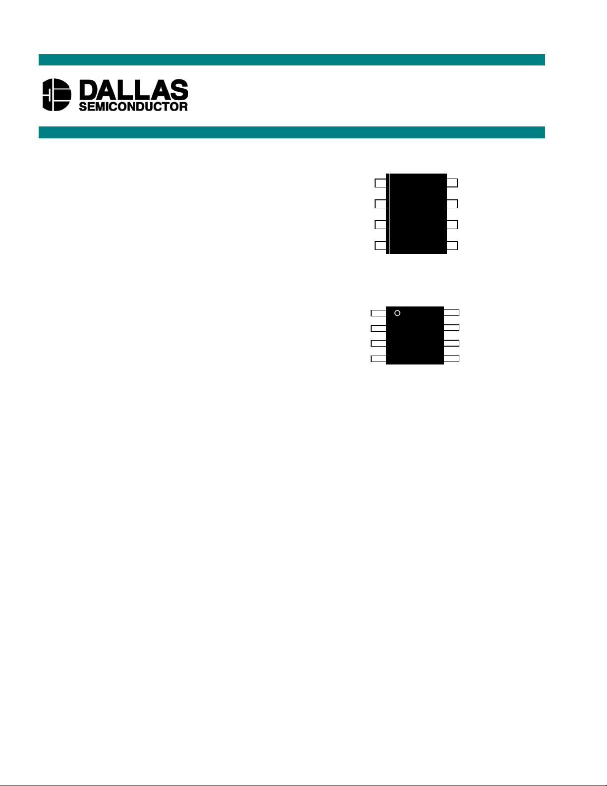
§ Available in 8-pin SO (150mil) and mSOP
packages
PIN ASSIGNMENT
DS1631Z
7
6
T
OUT
GND
2
L
3
DS1631Z—8-pin SO (150mil)
D1631
7
6
T
OUT
GND
2
L
3
DS1631U—mSOP
PIN DESCRIPTION
SDA - Open-Drain Data I/O
SCL - Clock Input
T
GND - Ground
V
A
A
A
- Thermostat Output
OUT
- Power Supply (2.7V to 5.5V)
DD
- Address Input
0
- Address Input
1
- Address Input
2
V
DD
A
0
A
1
A
2
V
DD
A
0
A
1
A
2
DESCRIPTION
The DS1631 digital thermometer and thermostat provides 9-, 10-, 11-, or 12-bit digital temperature
readings over a range of -55°C to +125°C. The thermometer accuracy is ±0.5°C from 0°C to +70°C with
3.0V £ V
The thermostat output (T
thermostat trip point (T
£ 5.5V. The thermostat provides custom hysteresis with user-defined trip points (TH and TL).
DD
) becomes active when the temperature of the device exceeds the upper
OUT
), and remains active until the temperature drops below the lower thermostat trip
H
point (TL).
The T
and TL registers and thermometer configuration settings are stored in NV EEPROM so the
H
DS1631 can be programmed prior to installation. Communication with the DS1631 is achieved through a
standard 2-wire serial interface.
1 of 14 012402
Page 2
DETAILED PIN DESCRIPTION Table 1
A
A
A1A2A
0
OU
PIN SYMBOL DESCRIPTION
1SDAData input/output pin for 2-wire serial communication port. Open drain.
2SCLClock input pin for 2-wire serial communication port.
3T
OUT
4 GND
5A
6A
7A
2
1
0
Thermostat output pin. Push-pull.
Ground pin.
Address input pin.
Address input pin.
Address input pin.
8VDDSupply Voltage. 2.7V to 5.5V input power pin.
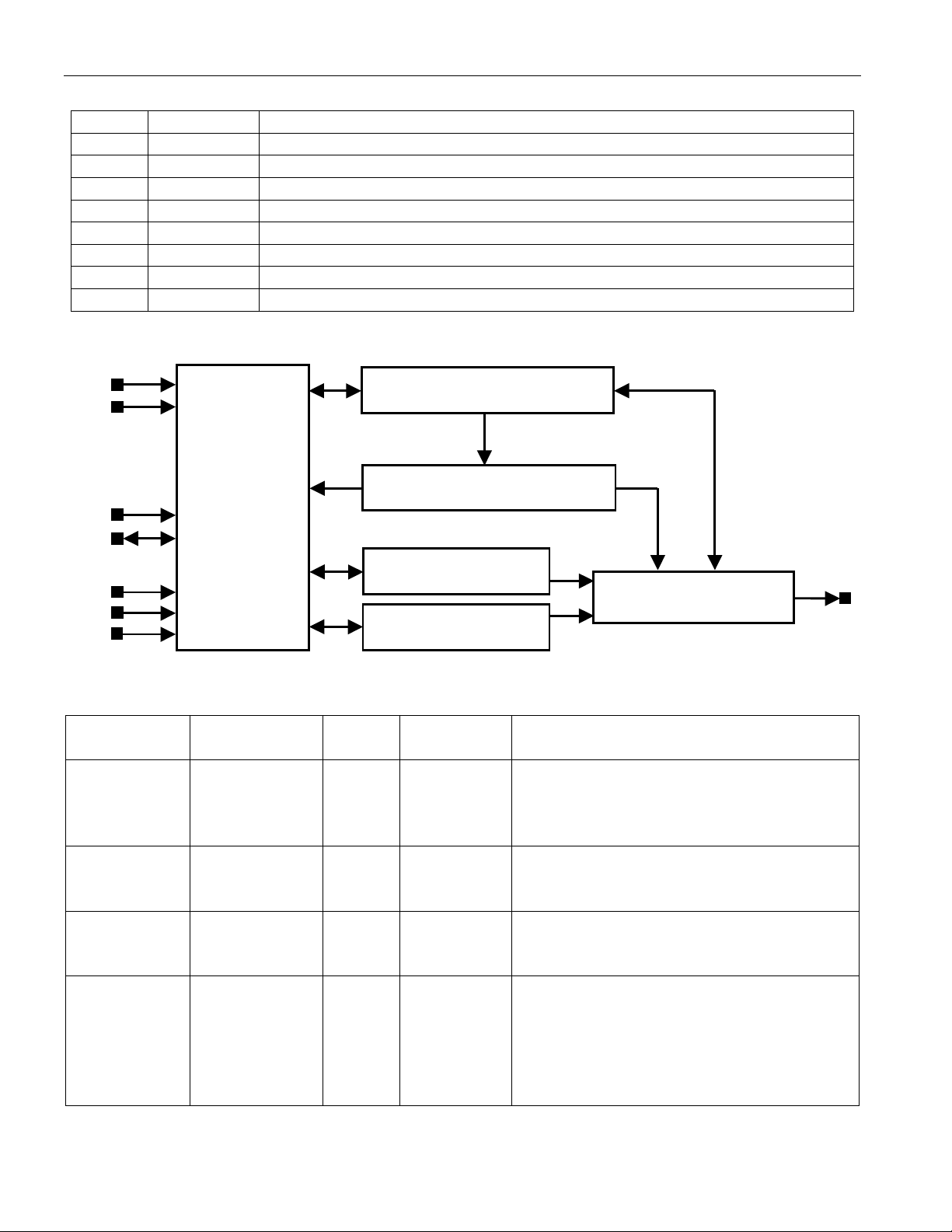
DS1631 FUNCTIONAL BLOCK DIAGRAM Figure 1
DS1631
V
GND
SCL
SD
ADDRESS
AND
I/O CONTROL
CONFIGURATION REGISTER
ND CONTROL LOGIC
TEMPERATURE SENSOR
TH REGISTER
REGISTER
T
L
DIGITAL
COMPARATOR/LOGIC
DS1631 REGISTER SUMMARY Table 2
REGISTER
NAME
Temperature (Read Only) 2 bytes SRAM Measured temperature in two’s complement
T
H
T
L
Configuration (Read/
USER
ACCESS
(Read/
Write)
(Read/
Write)
Write, but
some bits are
Read Only—
see Table 5)
SIZE MEMORY
TYPE
REGISTER CONTENTS
AND POWER-UP/POR STATE
format.
Power-up/POR state: -60ºC (1100 0100
0000 0000)
2 bytes EEPROM Upper alarm trip point in two’s complement
format.
Power-up/POR state: user defined.
2 bytes EEPROM Lower alarm trip point in two’s
complement format.
Power-up/POR state: user defined.
1 byte SRAM and
EEPROM
Configuration and status information.
Unsigned data.
6 MSbs = SRAM
2 LSbs (POL and 1SHOT bits) = EEPROM
Power-up/POR state: 100011XX (XX =
User defined)
T
T
2 of 14
Page 3

DS1631
OVERVIEW
The DS1631 measures temperature using a bandgap-based temperature sensor. A delta-sigma analog-todigital converter (ADC) converts the measured temperature to a 9-, 10-, 11-, or 12-bit (user-selectable)
digital value that is calibrated in degrees centigrade; for Fahrenheit applications a lookup table or
conversion routine must be used. The DS1631 also provides thermostat capability with userprogrammable NV trip-point registers. Communication with the DS1631 is achieved through a standard
2-wire serial interface.
Detailed DS1631 pin descriptions are provided in Table 1 and user-accessible registers are summarized in
Table 2.
Note: The DS1631 is software- and pin-compatible with DS1621. This compatibility covers all
functions/commands described in the DS1621 data sheet including access to the Count_Remain and
Count_Per_C registers for high-resolution temperature calculations based on the legacy dual-oscillator
architecture. Refer to Application Note 176 Using the DS1631 in DS1621 Applications for more
information.
OPERATION—MEASURING TEMPERATURE
The DS1631 can be programmed to take continuous temperature measurements (continuous conversion
mode) or to take single temperature measurements on command (one-shot mode). The measurement
mode is programmed through the 1SHOT bit in the configuration register: 1SHOT = 1—one-shot mode;
1SHOT = 0—continuous conversion mode. The 1SHOT bit is stored in NV EEPROM, so it can be
programmed prior to installation if desired. In continuous conversion mode, when a Start Convert T
command is issued, the DS1631 will perform consecutive temperature measurements until a Stop Convert
T command is issued. In one-shot mode, the Start Convert T command causes one temperature
measurement to be taken, then the DS1631 returns to a low-power idle state. One-shot mode is
recommended for use in power-sensitive applications.
The resolution of the DS1631 digital temperature data is user-configurable to 9, 10, 11, or 12 bits,
corresponding to temperature increments of 0.5°C, 0.25°C, 0.125°C, and 0.0625°C, respectively. The
default resolution at power-up is 12 bits, and it can be changed through the R0 and R1 bits in the
configuration register as explained in the CONFIGURATION REGISTER section of this data sheet. Note
that the conversion time doubles for each additional bit of resolution.
After each temperature measurement and analog-to-digital conversion, the DS1631 stores the temperature
as a 16-bit two’s complement number in the 2-byte temperature register (see Figure 2). The sign bit (S)
indicates if the temperature is positive or negative: for positive numbers S = 0 and for negative numbers S
= 1. The Read Temperature command provides user access to the temperature register.
Bits 3 through 0 of the temperature register are hardwired to 0. When the DS1631 is configured for 12-bit
resolution, the 12 MSbs (bits 15 through 4) of the temperature register will contain temperature data. For
11-bit resolution, the 11 MSbs (bits 15 through 5) of the temperature register will contain data, and bit 4
will read out as 0. Likewise, for 10-bit resolution, the 10 MSbs (bits 15 through 6) will contain data, and
for 9-bit the 9 MSbs (bits 15 through 7) will contain data, and all unused LSbs will contain 0s. Table 3
gives examples of 12-bit resolution digital output data and the corresponding temperatures.
3 of 14
Page 4
TEMPERATURE, TH, and TL REGISTER FORMAT Figure 2
bit 15 bit 14 bit 13 bit 12 bit 11 bit 10 bit 9 bit 8
MS Byte
LS Byte
S2
bit 7 bit 6 bit 5 bit 4 bit 3 bit 2 bit 1 bit 0
-1
2
6
-2
2
5
2
-3
2
4
2
-4
2
3
2
2
2
1
2
0000
12-BIT RESOLUTION TEMPERATURE/DATA RELATIONSHIP Table 3
DS1631
0
2
TEMPERATURE
(°C)
DIGITAL OUTPUT
(BINARY)
DIGITAL OUTPUT
(HEX)
+125 0111 1101 0000 0000 7D00h
+25.0625 0001 1001 0001 0000 1910h
+10.125 0000 1010 0010 0000 0A20h
+0.5 0000 0000 1000 0000 0080h
0 0000 0000 0000 0000 0000h
-0.5 1111 1111 1000 0000 FF80h
-10.125 1111 0101 1110 0000 F5E0h
-25.0625 1110 0110 1111 0000 E6F0h
-55 1100 1001 0000 0000 C900h
OPERATION—THERMOSTAT FUNCTION
The DS1631 thermostat output (T
updated value until the next conversion completes. T
defined upper and lower trip points. When the measured temperature meets or exceeds the value stored in
the upper trip-point register (TH), T
below the value stored in the lower trip-point register (TL) (see Figure 3). This allows the user to program
any amount of hysteresis into the output response. The active state of T
the polarity bit (POL) in the configuration register: POL = 1—T
active low.
) is updated after every temperature conversion, and remains at the
OUT
is activated and deactivated based on user-
OUT
will become active and stay active until the temperature falls
OUT
is user-programmable through
OUT
is active high; POL = 0—T
OUT
OUT
is
The user-defined values in the T
and TL registers (see Figure 2) must be in two’s complement format
H
with the MSb (bit 15) containing the sign bit (S). The resolution of the TH and TL values is determined by
the R0 and R1 bits in the configuration register (see Table 4), so the TH and TL resolution will match the
output temperature resolution. For example, for 10-bit resolution bits 5 through 0 of the TH and T
registers will read out as 0 (even if 1s are written to these bits), and the converted temperature will be
compared to the 10 MSbs of TH and TL.
The TH and TL registers and the POL bit are stored in EEPROM; therefore, they are NV and can be
programmed prior to installation of the DS1631. Writing to and reading from the T
, TL, and
H
configuration registers is achieved using the Access TH, Access TL, and Access Config commands.
Another thermostat feature is the temperature high and low flags (THF and TLF) in the configuration
register. These bits provide a record of whether the temperature has been greater than TH or less than T
at anytime since the DS1631 was powered up. If the temperature ever exceeds the TH register value, the
THF bit in the configuration register will be set to 1, and if the temperature ever falls below the T
value,
L
the TLF bit in the configuration register will be set to 1. Once THF and/or TLF has been set, it will
remain set until over-written with a 0 by the user or until the power is cycled.
4 of 14
L
L
Page 5
THERMOSTAT OUTPUT OPERATION Figure 3
b
b
b
b
b
b
g
DS1631
Lo
ic 1
Logic 0
POL=1 (T
T
L
is active high)
OUT
T
OUT
T
H
Temp
CONFIGURATION REGISTER
The configuration register allows the user to program various DS1631 options such as conversion
resolution, T
polarity, and operating mode. It also provides information to the user about conversion
OUT
status, EEPROM activity, and thermostat activity. The configuration register is arranged as shown in
Figure 4 and detailed descriptions of each bit are provided in Table 5. This register can be read from and
written to using the Access Config command. Note that the POL and 1SHOT bits are stored in EEPROM
and all other configuration register bits are SRAM.
CONFIGURATION REGISTER Figure 4
MSb
it 6
it 5
it 4
it 3
it 2
it 1 LSb
DONE THF TLF NVB R1 R0 POL* 1SHOT*
*NV (EEPROM)
RESOLUTION CONFIGURATION Table 4
R1 R0 RESOLUTION CONVERSION
0 0 9-bit 93.75ms
0 1 10-bit 187.5ms
1 0 11-bit 375ms
1 1 12-bit 750ms
START, STOP, AND ACK SIGNALS Figure 5
SDA
SCL
TIME (MAX)
START
Condition
5 of 14
ACK (or NACK)
From Receiver
STOP
Condition
Page 6

CONFIGURATION REGISTER BIT DESCRIPTIONS Table 5
BIT NAME
(USER ACCESS)
DONE—Temperature
Conversion Done
(Read Only)
THF—Temperature High Flag
(Read/Write)
TLF—Temperature Low Flag
(Read/Write)
NVB—NV Memory
Busy
(Read Only)
R1—Resolution Bit 1
(Read/Write)
R0—Resolution Bit 0
(Read/Write)
POL*— T
Polarity
OUT
(Read/Write)
1SHOT*— Conversion Mode
(Read/Write)
*Stored in EEPROM
Power-up/POR state = 1
DONE = 0—Temperature conversion is in progress.
DONE = 1—Temperature conversion is complete.
Power-up/POR state = 0.
THF = 0—The measured temperature has not exceeded the value
stored in the TH register since power-up.
THF = 1—At some point since power-up the measured temperature
has been higher than the value stored in the TH register. THF will
remain a 1 until it is over-written with a 0 by the user or until the
power is cycled.
Power-up/POR state = 0
TLF = 0—The measured temperature has not been lower than the
value stored in the TL register since power-up.
TLF = 1—At some point since power-up the measured temperature
has been lower than the value stored in the TL register. TLF will
remain a 1 until it is over-written with a 0 by the user or until the
power is cycled.
Power-up/POR state = 0
NVB = 1—A write to EEPROM memory is in progress
NVB = 0—NV memory is not busy.
Power-up/POR state = 1
Used to set conversion, TH, and TL resolution (see Table 4)
Power-up/POR state = 1
Used to set conversion, TH, and TL resolution (see Table 4)
Power-up/POR state = last value written to this bit
POL = 1—T
POL = 0—T
Power-up/POR state = last value written to this bit
1SHOT = 1—One-shot mode. The Start Convert T command will
cause a single temperature conversion and then the device will return
to a low-power standby state.
1SHOT = 0—Continuous conversion mode. The Start Convert T
command will initiate continuous temperature conversions.
FUNCTIONAL DESCRIPTION
is active high.
OUT
is active low.
OUT
DS1631
6 of 14
Page 7

DS1631
2-WIRE SERIAL DATA BUS
The DS1631 communicates over a standard bidirectional 2-wire serial data bus that consists of a serial
clock (SCL) signal and serial data (SDA) signal. The DS1631 interfaces to the bus through the SCL input
pin and open-drain SDA I/O pin.
The following terminology is used to describe 2-wire communication:
Master Device: Microprocessor/microcontroller that controls the slave devices on the bus. The master
device generates the SCL signal and START and STOP conditions.
Slave: All devices on the bus other than the master. The DS1631 always functions as a slave.
Bus Idle or Not Busy: Both SDA and SCL remain high. SDA is held high by a pullup resistor when the
bus is idle, and SCL must either be forced high by the master (if the SCL output is push-pull) or pulled
high by a pullup resistor (if the SCL output is open-drain).
Transmitter: A device (master or slave) that is sending data on the bus.
Receiver: A device (master or slave) that is receiving data from the bus.
START Condition: Indicates the beginning of a data transfer to all devices on the bus. The master
generates a START condition by pulling SDA from high to low while SCL is high (see Figure 5). A
repeated START is sometimes used at the end of a data transfer (instead of a STOP) to indicate that the
master will perform another operation.
STOP Condition: Indicates the end of a data transfer to all devices on the bus. The master generates a
STOP condition by transitioning SDA from low to high while SCL is high (see Figure 5). After the
STOP is issued, the master releases the bus to its idle state.
Acknowledge (ACK): When a device (either master or slave) is acting as a receiver, it must generate an
acknowledge (ACK) on the SDA line after receiving every byte of data. The receiving device performs an
ACK by pulling the SDA line low for an entire SCL period (see Figure 5). During the ACK clock cycle,
the transmitting device must release SDA. A variation on the ACK signal is the “not acknowledge”
(NACK). When the master device is acting as a receiver, it uses a NACK instead of an ACK after the last
data byte to indicate that it is finished receiving data. The master indicates a NACK by leaving the SDA
line high during the ACK clock cycle.
Slave Address: Every slave device on the bus must have a unique 7-bit address that allows the master to
access that device. The DS1631’s 7-bit bus address is as follows:
bit 6 bit 5 bit 4 bit 3 bit 2 bit 1 bit 0
1001A2A
A
1
0
where bits 2, 1, and 0 are user selectable through the A2, A1, and A0 pins. The three user-selectable
address bits allow up to eight DS1631s to be multi-dropped on the same bus.
Control Byte: The control byte is transmitted by the master and consists of the 7-bit slave address plus a
read/write (R/W¯¯) bit. If the master is going to read data from the slave device then R/W¯¯ = 1, and if the
master is going to write data to the slave device then R/W¯¯ = 0.
Command Byte: The command byte can be any of the command protocols described in the DS1631
COMMAND SET section of this data sheet.
7 of 14
Page 8

DS1631
GENERAL 2-WIRE INFORMATION
§ All data is transmitted MSb first over the 2-wire bus.
§ A pullup resistor is required on the SDA line and, when the bus is idle, both SDA and SCL must remain
in a logic-high state.
§ All bus communication must be initiated with a START condition and terminated with a STOP
condition. During a START or STOP is the only time SDA is allowed to change states while SCL is
high. At all other times, changes on the SDA line can only occur when SCL is low: SDA must remain
stable when SCL is high.
§ One bit of data is transmitted on the 2-wire bus each SCL period.
§ After every 8-bit (1-byte) transfer, the receiving device must answer with an ACK (or NACK), which
takes one SCL period. Therefore, nine clocks are required for every one byte data transfer.
INITIATING COMMUNICATION WITH THE DS1631
To initiate communication with the DS1631, the master must generate a START followed by a control
byte containing the DS1631 bus address. The R/W¯¯ bit of the control byte must be a 0 (“write”) since the
master must next write a command byte to the DS1631. The DS1631 will respond with an ACK after
receiving the control byte. This must be followed by a command byte from the master, which tells the
DS1631 what type of operation is to be performed. The DS1631 will again respond with an ACK after
receiving the command byte.
If the command byte is a Start Convert T or Stop Convert T command (see Figure 6a), the transaction is
finished, and the master must issue a STOP to signal the end of the communication sequence. If the
command byte indicates a write or read operation, additional actions must occur as explained in the
following sections.
2-WIRE WRITES
The master can write data to the DS1631 by issuing an Access Config, Access TH, or Access TL
command following the control byte (see Figures 6b and 6d). Since the R/W¯¯ bit in the control byte was a
0 (“write”), the DS1631 is already prepared to receive data. Therefore, after the DS1631 sends an ACK in
response to the command byte, the master device can immediately begin transmitting data to the DS1631.
When writing to the configuration register, the master must send one byte of data, and when writing to the
or TL registers the master must send two bytes of data. After receiving each data byte, the DS1631 will
T
H
respond with an ACK, and the transaction is finished with a STOP from the master.
2-WIRE READS
The master can read data from the DS1631 by issuing an Access Config, Access TH, Access TL, or Read
Temperature command following the control byte (see Figures 6c and 6e). After the DS1631 sends an
ACK in response to the command, the master must generate a repeated START followed by a control
byte with the same DS1631 address as the first control byte. However, this time the R/
which tells the DS1631 that a “read” is being performed. After the DS1631 sends an ACK in response to
the control byte, it will begin transmitting the requested data on the next clock cycle, provided the master
continues to generate the clock signal on SCL. When reading from the configuration register, the DS1631
will transmit one byte of data, after which the master must respond with a NACK followed by a STOP.
For two-byte reads (i.e., from the temperature, TH or TL, register), the master must respond to the first
data byte with an ACK and to the second byte with a NACK, followed by a STOP. If only one byte of
temperature data is needed, the master can issue a NACK followed by a STOP after reading the first data
byte, and the DS1631 will quit transmitting data.
W¯¯ bit must be a 1,
8 of 14
Page 9

2-WIRE INTERFACE TIMING Figure 6
DS1631
P
N
STOP
NACK
(Master)
C1 C0
C2
C3
P
STOP
N
(Master)
NACK
D2 D1 D0
D3
Data Byte
(from DS1631)
D6 D5 D4
P
STOP
AD2D6 D5 D4
ACK
(DS1631)
D1 D0A0
D3
Data Byte
(from Master)
P
STOP
ACK
(DS1631)
ACK
(DS1631)
100AD7A2
1
D7
A
R
A2 A1 A0
00
S1 1
100
1
ACK
(DS1631)
Control Byte
Repeat
START
(DS1631)
ACK
D2 D0D7D6 D5 D4
D3
D4
D6 D5
A
D2 D1 D0D7 AD1
D3
AC7 C6 C5 C4
C1 C0
C3
P
STOP
ACK
(DS1631)
LS Data Byte
(from Master)
ACK
(DS1631)
MS Data Byte
(from Master)
ACK
(DS1631)
…
…
A
ACK
(Master)
D3
MS Data Byte
(from DS1631)
D7
AD2D1D0D6 D5 D4
ACK
R
A2 A1 A0
00
S 11
AC4
C0
C2 C1C7
C3
(DS1631)
Control Byte
START
Repeat
(DS1631)
ACK
…
D2 D1 D0
D3
D5
D6 D4
D7
…
LS Data Byte
(from DS1631)
a) Issue a "Start Convert T” or “Stop Convert T” Command
Command Byte
AC7C6C5C4 A
ACK
W
A2 A1 A0
00
S 11
SCL
SDA
(DS1631)
Control Byte
START
Command Byte
AA1 1 0 1 0
ACK
W
00
S 11
b) Write to the Configuration Register
SCL
SDA
(DS1631)
Control Byte
START
c) Read From the Configuration Register
SCL
010 A
A1S1 1
W
A2 A1 A0
00
SDA
Command Byte
ACK
(DS1631)
Register
L
or T
H
Control Byte
START
d) Write to the T
SCL
Command Byte
A
ACK
W
A2 A1 A0 C2
Control Byte
00
S 11
START
SDA
Register
L
, or T
H
(DS1631)
e) Read From the Temperature, T
SCL
Command Byte
C6 C5A2 A1 A0
A
ACK
W
00
S 11
SDA
(DS1631)
Control Byte
START
9 of 14
Page 10

DS1631
DS1631 COMMAND SET
The DS1631 command set is detailed below and is summarized in Table 6.
Start Convert T [ 51h ]
Initiates temperature conversions. If the part is in one-shot mode (1SHOT = 1), only one conversion will
be performed. In continuous mode (1SHOT = 0), continuous temperature conversions will be performed
until a Stop Convert T command is issued.
Stop Convert T [ 22h ]
Stops temperature conversions when the device is in continuous conversion mode (1SHOT = 0).
Read Temperature [ AAh ]
Reads last converted temperature value from the 2-byte temperature register.
Access TH [ A1h ]
Reads or writes the 2-byte TH register.
Access TL [ A2h ]
Reads or writes the 2-byte TL register.
Access Config [ ACh ]
Reads or writes the 1-byte configuration register.
Software POR [ 54h ]
Initiates a software power-on reset (POR).
DS1631 COMMAND SET Table 6
2-Wire Bus Activity
Command Description Protocol
TEMPERATURE
Start Convert T Initiates temperature
conversions.
Stop Convert T Halts temperature conversions. 22h Idle
Read
Temperature
Access TH Reads or writes the TH register. A1h Two data bytes are
Access TL Reads or writes the TL register. A2h Two data bytes are
Access Config Reads or writes the
Software POR Initiates a software power-on
Reads last converted
temperature value from
temperature register.
THERMOSTAT
configuration register.
OTHER
reset.
51h Idle
AAh Two data bytes are
ACh One data byte is
54h Idle
After Command is
Issued
transmitted by the
DS1631.
transmitted.
transmitted.
transmitted.
Notes
1
2, 3
2, 3
2, 3
10 of 14
Page 11

DS1631
NOTES:
1) If only one byte of temperature data is needed, the master can issue a NACK followed by a STOP
after reading the first data byte, and the DS1631 will quit transmitting data.
2) After issuing a write command, no further writes should be requested for at least 10ms due to the
EEPROM write cycle time.
3) Data direction depends upon R/ W bit in the 2-wire control byte.
DS1631 OPERATION EXAMPLE
In this example, the master configures the DS1631 (A1A2A3 = 000) for continuous conversions and
thermostatic function.
MASTER
MODE
DS1631
MODE
DATA
(MSb first) COMMENTS
TX RX START Master issues a START condition.
TX RX 90h Master sends control byte with R/W¯¯ = 0.
RX TX ACK DS1631 generates acknowledge bit.
TX RX ACh Master sends Access Config command.
RX TX ACK DS1631 generates acknowledge bit.
TX RX 02h Master writes a data byte to the configuration register to
put the DS1631 in continuous conversion mode and set the
T
polarity to active high.
OUT
RX TX ACK DS1631 generates acknowledge bit.
TX RX START Master generates a repeated START condition.
TX RX 90h Master sends control byte with R/W¯¯ = 0.
RX TX ACK DS1631 generates acknowledge bit.
TX RX A1h Master sends Access TH command.
RX TX ACK DS1631 generates acknowledge bit.
TX RX 28h Master sends most significant data byte for TH = +40°C.
RX TX ACK DS1631 generates acknowledge bit.
TX RX 00h Master sends least significant data byte for TH = +40°C.
RX TX ACK DS1631 generates acknowledge bit.
TX RX START Master generates a repeated START condition.
TX RX 90h Master sends control byte with R/W¯¯ = 0.
RX TX ACK DS1631 generates acknowledge bit.
TX RX A2h Master sends Access TL command.
RX TX ACK DS1631 generates acknowledge bit.
TX RX 0Ah Master sends most significant data byte for TL = +10°C.
RX TX ACK DS1631 generates acknowledge bit.
TX RX 00h Master sends least significant data byte for TL = +10°C.
RX TX ACK DS1631 generates acknowledge bit.
TX RX START Master generates a repeated START condition.
TX RX 90h Master sends control byte with R/W¯¯ = 0.
RX TX ACK DS1631 generates acknowledge bit.
TX RX 51h Master sends Start Convert T command.
RX TX ACK DS1631 generates acknowledge bit.
TX RX STOP Master issues a STOP condition.
11 of 14
Page 12

DS1631
ABSOLUTE MAXIMUM RATINGS*
Voltage on any Pin Relative to Ground -0.5V to +6.0V
Operating Temperature Range -55°C to +125°C
Storage Temperature Range -55°C to +125°C
Solder Dip Temperature (10s) +260°C
Reflow Oven Temperature +220°C
* These are stress ratings only and functional operation of the device at these or any other conditions
above those indicated in the operation sections of this specification is not implied. Exposure to absolute
maximum rating conditions for extended periods of time may affect reliability.
DC ELECTRICAL CHARACTERISTICS (-55°C to +125°C; V
= 2.7V to 5.5V)
DD
PARAMETER SYMBOL CONDITIONS MIN MAX UNITS NOTES
Supply Voltage V
Thermometer Error T
DD
ERR
0°C to +70°C
3.0V £ V
DD
0°C to +70°C
2.7V £ V
DD
£ 5.5V
< 3.0V
2.7 5.5 V 1
±½
°C 2
±1
-55°C to +125°C ±2
Low-Level Input
V
IL
-0.5 0.3V
DD
V
Voltage
High-Level Input
V
IH
0.7V
DD
VDD + 0.3 V
Voltage
Output Voltage
Input Current each
V
V
OL1
OL2
3mA sink current 0 0.4 VSDA Low-Level
6mA sink current 0 0.6 V
0.4 < V
< 0.9V
I/O
DD
-10 +10 µA
I/O pin
Active Supply
Current
I
DD
Temperature
conversion
1mA
-55°C to +85°C
Temperature
1.25 mA
conversion
+85°C to +125°C
E2 Write 400 µA
Communication only 110 µA
Standby Supply
I
STBY
0°C to +70°C 800 nA 4
Current
Output Logic
OUT
Voltage
V
V
OH
OL
1mA source current 2.4 V 1T
4mA sink current 0.4 V 1
3
NOTES:
1) All voltages are referenced to ground.
2) See Typical Curve (Figure 7).
3) Specified with T
4) Specified with temperature conversions stopped; T
and A
, A1, A2 = 0 or VDD.
0
pin open; VDD = 5V; A0, A1, A2 = 0 or VDD; and f
OUT
12 of 14
³ 2Hz.
SCL
pin open; VDD = 5V; SDA = VDD; SCL = VDD;
OUT
Page 13

EEPROM AC ELECTRICAL CHARACTERISTICS
(-55°C to +100°C; V
PARAMETER SYMBOL CONDITIONS MIN TYP MAX UNITS
EEPROM Write Cycle Time t
EEPROM Writes N
EEPROM Data Retention t
wr
EEWR
EEDR
-55°C to +55°C 50k writes
-55°C to +55°C 10 years
DS1631
= 2.7V to 5.5V)
DD
410ms
AC ELECTRICAL CHARACTERISTICS (-55°C to +125°C; V
= 2.7V to 5.5V)
DD
PARAMETER SYMBOL CONDITION MIN TYP MAX UNITS NOTES
Temperature
Conversion Time
t
TC
9-bit resolution 93.75
10-bit resolution 187.5
ms
11-bit resolution 375
12-bit resolution 750
SCL Frequency f
Bus Free Time
t
BUF
SCL
0 400 kHz
1.3 µs 1
Between a STOP and
START Condition
START and Repeated
t
HD:STA
0.6 µs 1, 2
START Hold Time
from Falling SCL
Low Period of SCL t
High Period of SCL t
Repeated START
LOW
HIGH
t
SU:STA
1.3 µs 1
0.6 µs 1
0.6 µs 1
Condition Setup Time
to Rising SCL
Data-Out Hold Time
t
HD:DAT
0 0.9 µs 1
from Falling SCL
Data-In Setup Time to
t
SU:DAT
100 ns 1
Rising SCL
Rise Time of SDA and
SCL
Fall time of SDA and
SCL
STOP Setup Time to
t
R
t
F
t
SU:STO
20 +
0.1C
20 +
0.1C
B
B
1000 ns 1, 3
300 ns 1, 3
0.6 µs 1
Rising SCL
Capacitive Load for
C
B
400 pF
each Bus Line
I/O Capacitance C
Input Capacitance C
Spike Pulse Width that
t
SP
I/O
I
050ns
10 pF
5pF
can be Suppressed by
Input Filter
All values referenced to V
= 0.9 VDD and V
IH
= 0.1 VDD.
IL
NOTES:
1) See timing diagram in Figure 8.
2) After this period the first clock pulse is generated.
3) For example, if CB = 300pF, then tR[min] = tF[min] = 50ns.
13 of 14
Page 14

TYPICAL PERFORMANCE CURVE Figure 7
0.5
0.4
0.3
0.2
DS1631
0.1
0
-0.1
-0.2
-0.3
-0.4
-0.5
-5 5 15253545556575
TIMING DIAGRAM Figure 8
-3
s
s
+3
Mean
Temperature (°C)
14 of 14
 Loading...