

Page 1
DS1624
Digital Thermometer and Memory
www.dalsemi.com
312
475
SDA
SCL
NC
GND
VDDA
0
A
1
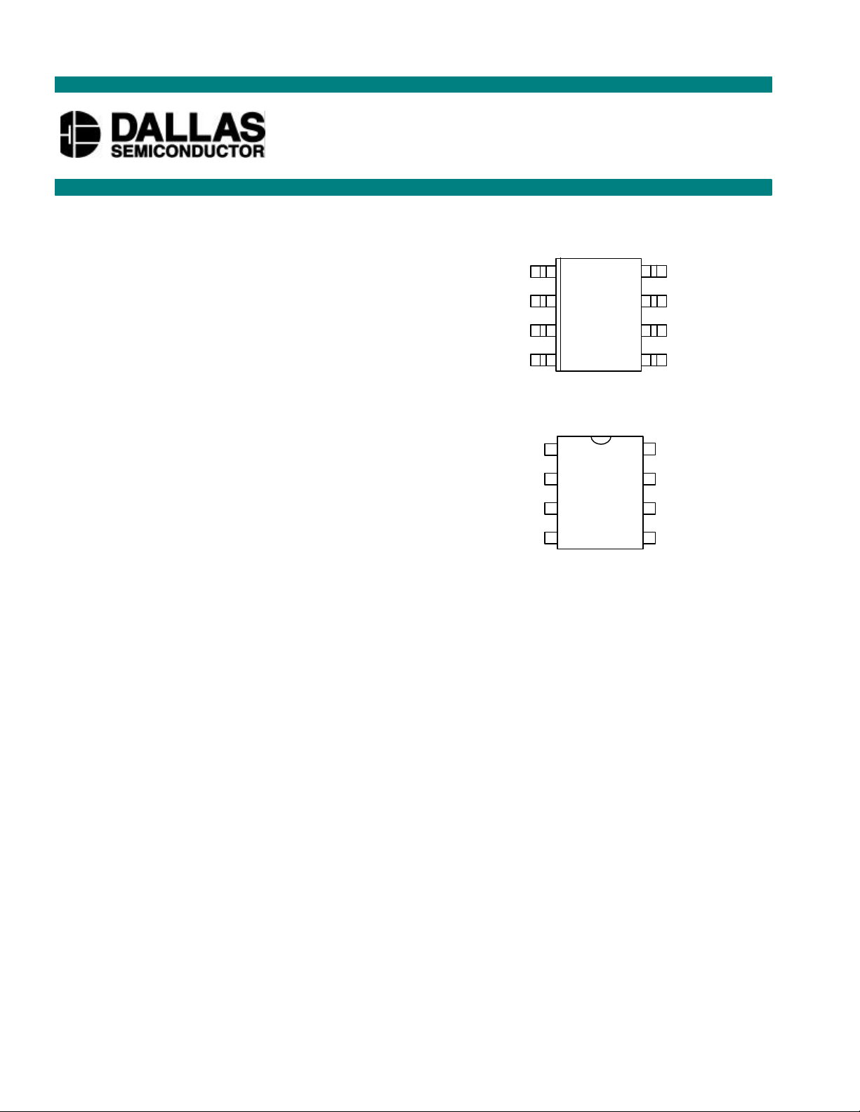
A2DS1624S 8-PIN SOIC (208 MIL)
312
4
8
5
SDA
SCL
NC
GND
VDDA
0
A
1
A2DS1624 8-PIN DIP (300 MIL)
FEATURES
§ Temperature measurements require no
external components
§ Measures temperatures from -55°C to +125°C
in 0.03125°C increments. Fahrenheit
equivalent is -67°F to +257°F in 0.05625°F
increments
§ Temperature is read as a 13-bit value (two
byte transfer)
§ Converts temperature to digital word in 1
second (max)
§ 256 bytes of E2 memory on board for storing
information such as frequency compensation
coefficients
§ Data is read from/written via a 2-wire serial
interface (open drain I/O lines)
§ Applications include temperature-
compensated crystal oscillators for test
equipment and radio systems
§ 8-pin DIP or SOIC packages
PIN ASSIGNMENT
6
See Mech Drawings Section
7
6
See Mech Drawings Section
PIN DESCRIPTION
SDA - 2-Wire Serial Data Input/Output
SCL - 2-Wire Serial Clock
GND - Ground
A0 - Chip Address Input
A1 - Chip Address Input
A2 - Chip Address Input
V
NC - No Connection
- Digital Power Supply (+3V - +5V)
DD
DESCRIPTION
The DS1624 consists of a digital thermometer and 256 bytes of E
13-bit temperature readings which indicate the temperature of the device. The E
store frequency compensation coefficients for digital correction of crystal frequency due to temperature.
Any other type of information may also reside in this user space.
2
memory. The thermometer provides
2
memory allows a user to
1 of 16 072099
Page 2
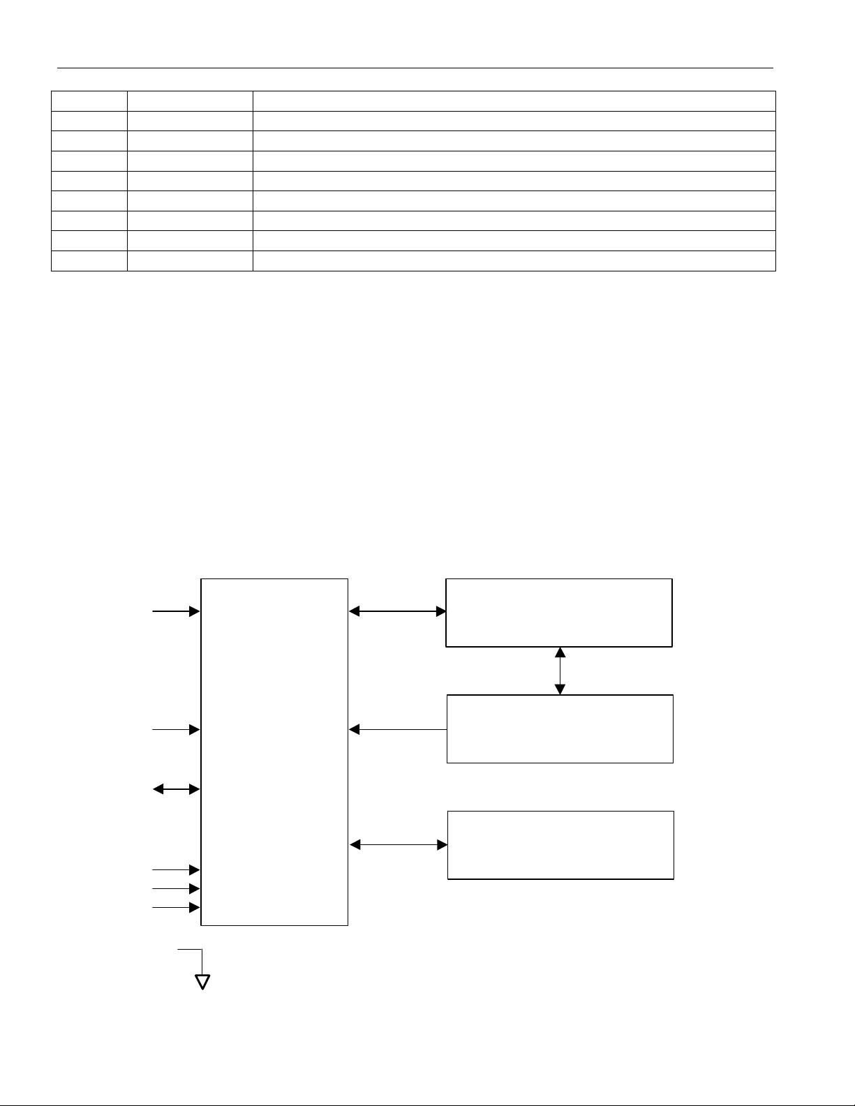
DS1624
STATUS REGISTER &
CONTROL LOGIC
TEMPERATURE SENSOR
EEPROM MEMORY (256 BYTES)
ADDRESS
V
DD
SCL
SDAA1A2
A0
GND
DETAILED PIN DESCRIPTION Table 1
PIN SYMBOL DESCRIPTION
1 SDA Data input/output pin for 2-wire serial communication port.
2 SCL Clock input/output pin for 2-wire serial communication port.
3 NC No connect. No Internal Connection.
4 GND
5 A2
6 A1
7 A0
8 V
DD
Ground pin.
Address input pin.
Address input pin.
Address input pin.
Supply Voltage 2.7V to 5.5V input power pin.
OVERVIEW
A block diagram of the DS1624 is shown in Figure 1. The DS1624 consists of two separate functional
units: 1) a 256–byte nonvolatile E
2
memory, and 2) a direct–to–digital temperature sensor.
The nonvolatile memory is made up of 256 bytes of E
2
memory. This memory may be used to store any
type of information the user wishes; for example, frequency compensation coefficients may be placed in
this memory to allow for compensation of measured frequency depending upon the temperature at which
the measurement is made. These memory locations are accessed through the 2–wire serial bus.
The direct to digital temperature sensor allows the DS1624 to measure the ambient temperature and
report the temperature value in a 13–bit word, with 0.03125°C resolution. The temperature sensor and its
related registers are accessed through the 2–wire serial interface.
DS1624 FUNCTIONAL BLOCK DIAGRAM Figure 1
AND
I/O CONTROL
2 of 16
Page 3

DS1624
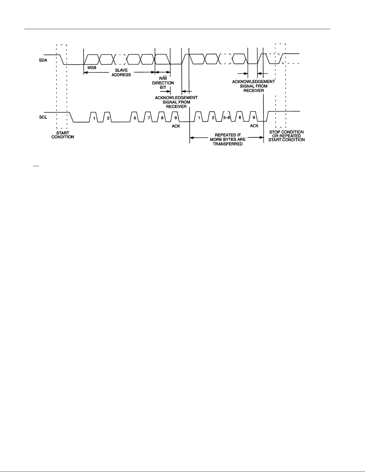
2-WIRE SERIAL DATA BUS
The DS1624 supports a bi–directional two–wire bus and data transmission protocol. A device that sends
data onto the bus is defined as a transmitter, and a device receiving data as a receiver. The device that
controls the message is called a “master”. The devices that are controlled by the master are “slaves”. The
bus must be controlled by a master device which generates the serial clock (SCL), controls the bus access,
and generates the START and STOP conditions. The DS1624 operates as a slave on the two–wire bus.
Connections to the bus are made via the open–drain I/O lines SDA and SCL. The following bus protocol
has been defined (See Figure 2):
• Data transfer may be initiated only when the bus is not busy.
• During data transfer, the data line must remain stable whenever the clock line is HIGH. Changes in
the data line while the clock line is high will be interpreted as control signals.
Accordingly, the following bus conditions have been defined:
Bus not busy: Both data and clock lines remain HIGH.
Start data transfer: A change in the state of the data line, from HIGH to LOW, while the clock is HIGH,
defines a START condition.
Stop data transfer: A change in the state of the data line, from LOW to HIGH, while the clock line is
HIGH, defines the STOP condition.
Data valid: The state of the data line represents valid data when, after a START condition, the data line
is stable for the duration of the HIGH period of the clock signal. The data on the line must be changed
during the LOW period of the clock signal. There is one clock pulse per bit of data.
Each data transfer is initiated with a START condition and terminated with a STOP condition The
number of data bytes transferred between START and STOP conditions is not limited, and is determined
by the master device. The information is transferred byte–wise and each receiver acknowledges with a
ninth bit.
Within the bus specifications a regular mode (100 KHz clock rate) and a fast mode (400 KHz clock rate)
are defined. The DS1624 works in both modes.
Acknowledge: Each receiving device, when addressed, is obliged to generate an acknowledge after the
reception of each byte. The master device must generate an extra clock pulse which is associated with this
acknowledge bit.
A device that acknowledges must pull down the SDA line during the acknowledge clock pulse in such a
way that the SDA line is stable LOW during the HIGH period of the acknowledge related clock pulse. Of
course, setup and hold times must be taken into account. A master must signal an end of data to the slave
by not generating an acknowledge bit on the last byte that has been clocked out of the slave. In this case,
the slave must leave the data line HIGH to enable the master to generate the STOP condition.
3 of 16
Page 4
DS1624
DATA TRANSFER ON 2-WIRE SERIAL BUS Figure 2
Figure 2 details how data transfer is accomplished on the two–wire bus. Depending upon the state of the
R/W bit, two types of data transfer are possible:
1. Data transfer from a master transmitter to a slave receiver. The first byte transmitted by the
master is the slave address. Next follows a number of data bytes. The slave returns an acknowledge
bit after each received byte.
2. Data transfer from a slave transmitter to a master receiver. The first byte (the slave
address) is transmitted by the master. The slave then returns an acknowledge bit. Next follows a
number of data bytes transmitted by the slave to the master. The master returns an acknowledge bit
after all received bytes other than the last byte. At the end of the last received byte, a ‘not
acknowledge’ is returned.
The master device generates all of the serial clock pulses and the START and STOP conditions. A
transfer is ended with a STOP condition or with a repeated START condition. Since a repeated START
condition is also the beginning of the next serial transfer, the bus will not be released.
The DS1624 may operate in the following two modes:
1. Slave receiver mode: Serial data and clock are received through SDA and SCL. After each byte is
received an acknowledge bit is transmitted. START and STOP conditions are recognized as the
beginning and end of a serial transfer. Address recognition is performed by hardware after reception
of the slave address and direction bit.
2. Slave transmitter mode: The first byte is received and handled as in the slave receiver mode.
However, in this mode the direction bit will indicate that the transfer direction is reversed. Serial data
is transmitted on SDA by the DS1624 while the serial clock is input on SCL. START and STOP
conditions are recognized as the beginning and end of a serial transfer.
SLAVE ADDRESS
A control byte is the first byte received following the START condition from the master device. The
control byte consists of a four bit control code; for the DS1624, this is set as 1001 binary for read and
write operations. The next three bits of the control byte are the device select bits (A2, A1, A0). They are
used by the master device to select which of eight devices are to be accessed. These bits are in effect the
4 of 16
Page 5
DS1624
three least significant bits of the slave address. The last bit of the control byte (R/W) defines the
operation to be performed. When set to a “1”, a read operation is selected, when set to a “0”, a write
operation is selected. Following the START condition the DS1624 monitors the SDA bus checking the
device type identifier being transmitted. Upon receiving the 1001 code and appropriate device select bits,
the slave device outputs an acknowledge signal on the SDA line.
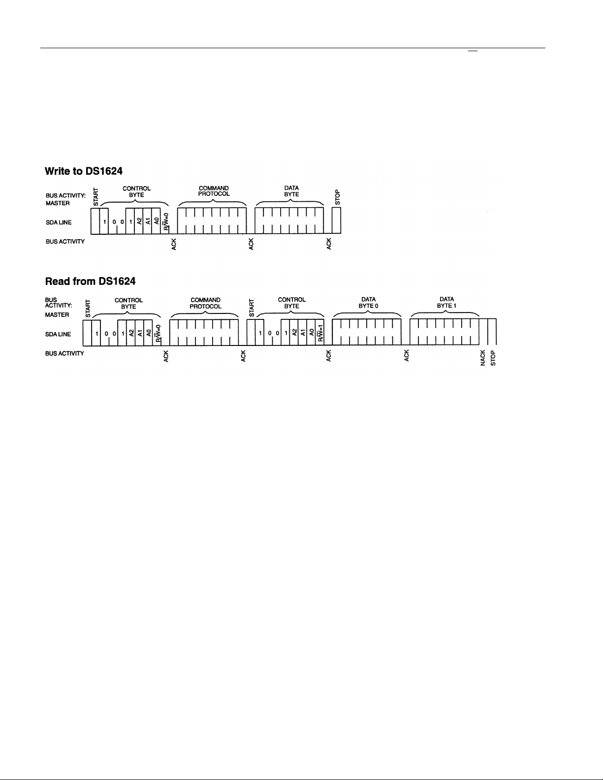
2-WIRE SERIAL COMMUNICATION WITH DS1624 Figure 3
OPERATION-MEASURING TEMPERATURE
A block diagram of the DS1624 is shown in Figure 1. The DS1624 measures temperatures through the
use of an on–board proprietary temperature measurement technique. A block diagram of the temperature
measurement circuitry is shown in Figure 4.
The DS1624 measures temperature by counting the number of clock cycles that an oscillator with a low
temperature coefficient goes through during a gate period determined by a high temperature coefficient
oscillator. The counter is preset with a base count that corresponds to –55 °C. If the counter reaches zero
before the gate period is over the temperature register, which is also preset to the –55°C value, is
incremented indicating that the temperature is higher than –55 °C.
At the same time, the counter is preset with a value determined by the slope accumulator circuitry. This
circuitry is needed to compensate for the parabolic behavior of the oscillators over temperature. The
counter is then clocked again until it reaches zero. If the gate period is still not finished, then this process
repeats.
The slope accumulator is used to compensate for the nonlinear behavior of the oscillators over
temperature, yielding a high resolution temperature measurement. This is done by changing the number
of counts necessary for the counter to go through for each incremental degree in temperature. To obtain
the desired resolution, both the value of the counter and the number of counts per °C (the value of the
slope accumulator) at a given temperature must be known.
5 of 16
Page 6

TEMPERATURE MEASURING CIRCUITRY Figure 4
LSB
SLOPE ACCUMULATOR
PRESET COMPARE
DS1624
LOW TEMPERATURE
COEFFICIENT OSCILLATOR
HIGH TEMPERATURE
COEFFICIENT OSCILLATOR
COUNTER PRESET
INC
=0
COUNTER
STOP
=0
TEMPERATURE REGISTER
SET/CLEAR
Internally, this calculation is performed by the DS1624 to provide 0.03125 °C resolution. The temperature
reading is provided in a 13–bit, two’s complement reading by issuing READ TEMPERATURE
command. Table 2 describes the exact relationship of output data to measured temperature. The data is
transmitted serially through the 2–wire serial interface, MSB first. The DS1624 can measure temperature
over the range of -55°C to +125°C in 0.03125°C increments. For Fahrenheit usage a lookup table or
conversion factor must be used.
TEMPERATURE/DATA RELATIONSHIPS Table 2
TEMP DIGITAL OUTPUT
(Binary)
+125°C 01111101 00000000 7D00h
+25.0625°C 00011001 00010000 1910h
+½°C 00000000 10000000 0080h
+0°C 00000000 00000000 0070h
-½°C 11111111 10000000 FF80h
-25.0625°C 11100110 11110000 E6F0h
-55°C 11001001 00000000 C900h
Since data is transmitted over the 2–wire bus MSB first, temperature data may be written to/read from the
DS1624 as either a single byte (with temperature resolution of 1 °C) or as two bytes, the second byte
containing the value of the 5 least significant bits of the temperature reading as shown in Table 1. Note
that the remaining three bits of this byte are set to all 0’s.
DIGITAL OUTPUT
(Hex)
6 of 16
Page 7

DS1624
0001010100010000LSB
MSB
Temperature is represented in the DS1624 in terms of a 0.03125 °C LSB, yielding the following 13–bit
format:
= +25.0625°C
OPERATION AND CONTROL
A configuration/status register is used to determine the method of operation of the DS1624 will use in a
particular application as well as indicating the status of the temperature conversion operation.
The configuration register is defined as follows:
CONFIGURATION/STATUS REGISTER
DONE 1 0 0 1 0 1 1SHOT
where
DONE = Conversion Done bit. “1” = Conversion complete, “0” = conversion in progress.
1SHOT = One Shot Mode. If 1SHOT is “1”, the DS1624 will perform one temperature conversion upon
receipt of the Start Convert T protocol. If 1SHOT is “0”, the DS1624 will continuously perform
temperature conversions. This bit is nonvolatile and the DS1624 is shipped with 1SHOT = “0”.
Since the configuration register is implemented in E2, writes to the register require 10 ms to complete.
After issuing a command to write to the configuration register, no further accesses to the DS1624 should
be made for at least 10 ms.
OPERATION – MEMORY
BYTE PROGRAM MODE
In this mode, the master sends addresses and one data byte to the DS1624.
Following a START condition, the device code (4–bit), the slave address (3 bit), and the R/W bit, which
is logic LOW, are placed onto the bus by the master. The master then sends the Access Memory protocol.
This indicates to the addressed DS1624 that a byte with a word address will follow after it has generated
an acknowledge bit. Therefore, the next byte transmitted by the master is the word address and will be
written into the address pointer of the DS1624. After receiving the acknowledge of the DS1624, the
master device transmits the data word to be written into the addressed memory location. The DS1624
acknowledges again and the master generates a STOP condition. This initiates the internal programming
cycle of the DS1624. A repeated START condition, instead of a STOP condition, will abort the
programming operation.
During the programming cycle the DS1624 will not acknowledge any further accesses to the device until
the programming cycle is complete (approximately 10 ms.)
7 of 16
Page 8

DS1624
PAGE PROGRAM MODE
To program the DS1624 the master sends addresses and data to the DS1624 which is the slave. This is
done by supplying a START condition followed by the 4–bit device code, the 3–bit slave address, and the
R/W bit which is defined as a logic LOW for a write. The master then sends the Access Memory
protocol. This indicates to the addressed slave that a word address will follow. The slave outputs the
acknowledge pulse to the master during the ninth clock pulse. When the word address is received by the
DS1624 it is placed in the address pointer defining which memory location is to be written. The DS1624
will generate an acknowledge after every 8–bits received and store them consecutively in an 8–byte RAM
until a STOP condition is detected which initiates the internal programming cycle.
A repeated START condition, instead of a STOP condition, will abort the programming operation.
During the programming cycle the DS1624 will not acknowledge any further accesses to the device until
the programming cycle is complete (approximately 10 ms).
If more than 8 bytes are transmitted by the master the DS1624 will roll over and overwrite the data
beginning with the first received byte. This does not affect erase/ write cycles of the EEPROM array and
is accomplished as a result of only allowing the address register’s bottom 3 bits to increment while the
upper 5 bits remain unchanged. The DS1624 is capable of 50,000 writes (25,000 erase/write cycles)
before EEPROM wear out may occur.
If the master generates a STOP condition after transmitting the first data word, byte programming mode
is entered.
READ MODE
In this mode, the master is reading data from the DS1624 E
address to the device with R/W set to “0”. The master then sends the Access Memory protocol and, after
receiving an acknowledge, then provides the word address, which is the address of the memory location
at which it wishes to begin reading. Note that while this is a read operation the address pointer must first
be written. During this period the DS1624 generates acknowledge bits as defined in the appropriate
section.
The master now generates another START condition and transmits the slave address. This time the R/
bit is set to “1” to put the DS1624 in read mode. After the DS1624 generates the acknowledge bit it
outputs the data from the addressed location on the SDA pin, increments the address pointer, and, if it
receives an acknowledge from the master, transmits the next consecutive byte. This auto-increment
sequence is only aborted when the master sends a STOP condition instead of an acknowledge. When the
address pointer reaches the end of the 256–byte memory space (address FFh) it will increment from the
end of the memory back to the first location of the memory (address 00h).
2
memory. The master first provides the slave
W
COMMAND SET
Data and control information is read from and written to the DS1624 in the format shown in Figure 3. To
write to the DS1624, the master will issue the slave address of the DS1624 and the R/W bit will be set to
“0”. After receiving an acknowledge the bus master provides a command protocol. After receiving this
protocol the DS1624 will issue an acknowledge then the master may send data to the DS1624. If the
DS1624 is to be read, the master must send the command protocol as before then issue a repeated START
condition and the control byte again, this time with the R/W bit set to “1” to allow reading of the data
from the DS1624. The command set for the DS1624 as shown in Table 3 is as follows:
8 of 16
Page 9

DS1624
Access Memory [17h]
This command instructs the DS1624 to access its E
byte is the value of the word address to be accessed. See OPERATION–MEMORY section for detailed
explanations of the use of this protocol and data format following it.
2
memory. After issuing this command, the next data
Access Config [ACh]
If R/W is “0”, this command writes to the configuration register. After issuing this command, the next
data byte is the value to be written into the configuration register. If R/W is “1”, the next data byte read is
the value stored in the configuration register.
Read Temperature [AAh]
This command reads the last temperature conversion result. The DS1624 will send two bytes in the
format described earlier, which are the contents of this register.
Start Convert T [EEh]
This command begins a temperature conversion. No further data is required. In one–shot mode the
temperature conversion will be performed and then the DS1624 will remain idle. In continuous mode this
command will initiate continuous conversions.
Stop Convert T [22h]
This command stops temperature conversion. No further data is required. This command may be used to
halt a DS1624 in continuous conversion mode. After issuing this command, the current temperature
measurement will be completed then the DS1624 will remain idle until a Start Convert T is issued to
resume continuous operation.
DS1624 COMMAND SET Table 3
2-WIRE BUS
DATA AFTER
ISSUING
INSTRUCTION DESCRIPTION PROTOCOL
PROTOCOL NOTES
TEMPERATURE CONVERSION COMMANDS
Read
Temperature
Reads last converted temperature
value from temperature register.
AAh <read 2 bytes
data>
Start Convert T Initiates temperature conversion. EEh idle 1
Stop Convert T Halts temperature conversion. 22h idle 1
THERMOSTAT COMMANDS
Access Memory Reads or writes to 256-byte
17h <write data> 2
EEPROM memory.
Access Config Reads or writes configuration data
ACh <write data> 2
to configuration register.
NOTES:
1. In continuous conversion mode a Stop Convert T command will halt continuous conversion. To
restart, the Start Convert T command must be issued. In one–shot mode a Start Convert T command
must be issued for every temperature reading desired.
2. Writing to the E
further reads or writes should be requested for at least 10 ms.
2
typically requires 10 ms at room temperature. After issuing a write command, no
9 of 16
Page 10

DS1624
During the programming cycle the DS1624 will not acknowledge any further accesses to the device until
the programming cycle is complete (approximately 10 ms).
MEMORY FUNCTION EXAMPLE
BUS MASTER
MODE
{Command protocol for configuration register}
{Start here}
TX RX START Bus Master Initiates a Start condition.
TX RX <cadr,0> Bus Master sends DS1624 address;
RX TX ACK DS1624 generates acknowledge bit.
TX RX ACh Bus Master sends Access Config
RX TX ACK DS1624 generates acknowledge bit. 1
TX RX 00h Bus Master sets up DS1624 for continuous
RX TX ACK DS1624 generates acknowledge bit. 2, 4
TX RX STOP Bus Master initiates the STOP condition.
{Command protocol for Start Convert T}
{Start here}
TX RX START Bus Master initiates a Start condition.
TX RX <cadr,0> Bus Master sends DS1624 address;
RX TX ACK DS1624 generates acknowledge bit.
TX RX EEh Bus Master sends Start Convert T
RX TX ACK DS1624 generates acknowledge bit. 1
TX RX STOP Bus Master initiates the STOP condition.
{Command protocol for reading the Temperature}
{Start here}
TX RX START Bus Master initiates a Start condition.
TX RX <cadr,0> Bus Master sends DS1624 address;
RX TX ACK DS1624 generates acknowledge bit.
TX RX AAh Bus Master sends Read Temp command
RX TX ACK DS1624 generates acknowledge bit. 1
TX RX START Bus Master initiates a Repeated Start
TX RX <cadr,1> Bus Master sends DS1624 address;
RX TX ACK DS1624 generates acknowledge bit.
RX TX <data> DS1624 sends the MSB byte of
TX RX ACK Bus Master generates acknowledge bit.
RX TX <data> DS1624 sends the LSB byte of
DS1624
MODE
DATA (MSB
FIRST)
COMMENTS NOTES
R/W=”0”;
command protocol.
conversion.
R/W=0;
command protocol.
R/W=0;
protocol.
condition.
R/W=1;
Temperature.
Temperature.
10 of 16
Page 11

BUS MASTER
MODE
DS1624
MODE
DATA (MSB
FIRST)
TX RX NACK Bus Master sends “NO
TX RX STOP Bus Master initiates the STOP condition.
{Command protocol for writing to EEPROM}
{Start here}
TX RX START Bus Master initiates a Start condition.
TX RX <cadr,0> Bus Master sends DS1624 address;
RX TX ACK DS1624 generates acknowledge bit.
TX RX 17h Bus Master sends Access Memory
RX TX ACK DS1624 generates acknowledge bit. 1
TX RX <madr> Bus Master sets the starting memory
RX TX ACK DS1624 generates acknowledge bit.
TX RX <data> Bus Master sends the first byte of data.
RX TX ACK DS1624 generates acknowledge bit.
TX RX <data> Bus Master sends the second byte of data.
RX TX ACK DS1624 generates acknowledge bit.
. . . .
. . . .
. . . .
. . . .
TX RX <data> Bus Master sends the n-th byte of data. 3
RX TX ACK DS1624 generates acknowledge bit.
TX RX STOP Bus Master initiates the STOP condition. 2, 4
{Command protocol for reading from EEPROM}
{Start here}
TX RX START Bus Master initiates a Start condition.
TX RX <cadr,0> Bus Master sends DS1624 address;
RX TX ACK DS1624 generates acknowledge bit.
TX RX 17h Bus Master sends Access Memory
RX TX ACK DS1624 generates acknowledge bit. 1
TX RX <madr> Bus Master sends the starting memory
RX TX ACK DS1624 generates acknowledge bit.
TX RX START Bus Master initiates a Repeated Start
TX RX <cadr,1> Bus Master sends DS1624 address;
RX TX ACK DS1624 generates acknowledge bit.
RX TX <data> DS1624 sends the first byte of data.
TX RX ACK Bus Master generates acknowledge bit.
DS1624
COMMENTS NOTES
ACKNOWLEDGE” bit.
R/W=0;
command protocol.
address.
R/W=0;
command protocol.
address.
condition.
R/W=1;
11 of 16
Page 12

DS1624
BUS MASTER
MODE
RX TX <data> DS1624 sends the second byte of data.
TX RX ACK Bus Master generates acknowledge bit.
. . . .
. . . .
. . . .
. . . .
RX TX <data> DS1624 sends the n-th byte of data. 5
TX RX NACK Bus Master send “NO KWOWLEDGE”
TX RX STOP Bus Master initiates the STOP condition.
DS1624
MODE
DATA (MSB
FIRST)
COMMENTS NOTES
bit.
NOTES:
1. If this protocol follows a write and the DS1624 does not acknowledge here, restart the protocol at the
Start here. If it does acknowledge, continue on.
2. Wait for write to complete (10 ms typ. 50 ms max). If DS1624 does not acknowledge the command
protocol immediately following a configure register or write mem protocol, the DS1624 has not
finished writing. Restart the new command protocol until the DS1624 acknowledges.
3. If n is greater than eight, the last eight bytes are the only bytes saved in memory. If the starting
address is 00 and the incoming data is 00 11 22 33 44 55 66 77 88 99, the result will be mem00=88
mem01=99 mem02=22 mem03=33 mem04=44 mem05=55 mem06=66 mem07=77. The data wraps
around and overwrites itself.
4. The STOP condition causes the DS1624 to initiate the write to EEPROM sequence. If a START
condition comes instead of the STOP condition, the write is aborted. The data is not saved.
5. For reading, the address is incremented. If the starting address is 04h and 30 bytes of data are read
out, 21h is the final address read.
ABSOLUTE MAXIMUM RATINGS*
Voltage on Any Pin Relative to Ground –0.5V to +7.0V
Operating Temperature –55°C to +125°C
Storage Temperature –55°C to +125°C
Soldering Temperature 260°C for 10 seconds
* This is a stress rating only and functional operation of the device at these or any other conditions above
those indicated in the operation sections of this spe cification is not implied. Exposure to absolute
maximum rating conditions for extended periods of time may affect reliability.
12 of 16
Page 13

DS1624
DD
DD
RECOMMENDED DC OPERATING CONDITIONS
PARAMETER SYMBOL MIN TYP MAX UNITS NOTES
Supply Voltage V
DD
2.7 5.0 5.5 V 1
DC ELECTRICAL CHARACTERISTICS (-55°C to +125°C; VDD=2.7V to 5.5V)
PARAMETER SYMBOL CONDITION MIN TYP MAX UNITS NOTES
±½Thermometer Error T
VDD+
0.5
10 pF
1000
100
°C 10
V
V
Low Level Input Voltage V
High Level Input Voltage V
Pulse width of spikes
which must be
suppressed by the input
filter
V
Voltage
V
Input Current each I/O
pin
I/O Capacitance C
Active Supply Current I
Standby Supply Current I
STBY
ERR
t
SP
OL1
OL2
I/O
CC
IL
IH
0°C to 70°C
-55°C to +0°C
and +70°C to
+125°C
See Typical Curve
-0.5 0.3V
0.7V
Fast Mode 0 50 ns
3 mA sink
0 0.4 VLow Level Output
current
6 mA sink
0 0.6 V
current
0.4<V
<0.9V
I/O
DD
-10 +10 µA 2
Temperature
Coversion
E2 Write 400 µA 3, 4
Communica-
tion Only
1 3 µA 3, 4
13 of 16
Page 14

DS1624
AC ELECTRICAL CHARACTERISTICS (-55°C to +125°C; VDD=2.7V to 5.5V)
PARAMETERS SYMBOL CONDITION MIN TYP MAX UNITS NOTES
Temperature
Conversion Time
NV Write Cycle
Time
SLK Clock
Frequency
Bus Free Time
Between a
STOP and START
Condition
Hold Time
(Repeated)
START Condition
Low Period of
SCL Clock
High Period of
SCL Clock
Setup Time for a
Repeated
START Condition
Data Hold Time t
Data Setup Time t
Rise Time of both
SDA and
SCL Signals
Fall Time of both
SDA and
SCL Signals
Setup Time for
STOP
Condition
Capacitive Load
for each Bus
Line
All values referred to VIH=0.9 VDD and VIL=0.1 VDD.
T
TC
t
WR
f
SCL
t
BUF
t
HD:STA
t
LOW
t
HIGH
t
SU:STA
HD:DAT
SU:DAT
t
R
t
F
t
SU:STO
C
b
400 1000 ms
0°C to 70°C 10 50 ms 9
Fast Mode
Standard Mode
Fast Mode
Standard Mode
Fast Mode
Standard Mode
Fast Mode
Standard Mode
Fast Mode
Standard Mode
Fast Mode
Standard Mode
Fast Mode
Standard Mode
Fast Mode
Standard Mode
Fast Mode
Standard Mode
Fast Mode
Standard Mode
Fast Mode
Standard Mode
0
0
1.3
4.7
0.6
4.0
1.3
4.7
0.6
4.0
0.6
4.7
0
0
100
250
20+0.1C
20+0.1C
0.6
4.0
400
KHz
100
µs
µs 5
µs
µs
µs
0.9 µs 6
ns 7
B
300
ns 8
1000
B
300
ns 8
300
µs
400 pF
14 of 16
Page 15

DS1624
AC ELECTRICAL CHARACTERISTICS (-55°C to +125°C; VDD=2.7V to 5.5V)
PARAMETER SYMBOL MIN TYP MAX UNITS NOTES
Input Capacitance C
I
5 pF
NOTES:
1. All voltages are referenced to ground.
2. I/O pins of fast mode devices must not obstruct the SDA and SCL lines if V
3. I
4. I
specified with SDA pin open.
CC
specified with VCC at 5.0V and SDA, SCL = 5.0V, 0°C to 70°C.
CC
is switched off.
DD
5. After this period, the first clock pulse is generated.
6. The maximum t
HD:DAT
has only to be met if the device does not stretch the LOW period ( t
LOW
) of the
SCL signal.
7. A fast mode device can be used in a standard mode system, but the requirement t
SU:DAT
>250 ns must
then be met. This will automatically be the case if the device does not stretch the LOW period of the
SCL signal. If such a device does stretch the LOW period of the SCL signal, it must output the next
data bit to the SDA line t
RMAX+tSU:DAT
= 1000+250 = 1250 ns before the SCL line is released.
8. Cb – total capacitance of one bus line in pF.
9. Writing to the nonvolatile memory should only take place in the 0°C to 70°C temperature range.
10. See Typical Curve for specification limits outside the 0°C to 70°C temperature range. Thermometer
error reflects sensor accuracy as tested during calibration.
TIMING DIAGRAMS
15 of 16
Page 16

TYPICAL PERFORMANCE CURVE
DS1624 DIGITAL THERMOMETER AND THERMOSTAT
TEMPERATURE READING ERROR
DS1624
TEMPERATURE (deg. C)
16 of 16
 Loading...