

Page 1
A
A
A
A
r
www.maxim-ic.com
www.maxim-ic.com
DS1616
Temperature and Three-Input
Muxed 8-Bit Data Recorde
FEATURES
§ Measures four channels of data:
- Integrated 8-bit temperature sensor
- Integrated 8-bit analog-to-digital
converter (ADC) with a three-input mux
§ Digital thermometer measures temperature
-40°C to +85°C in +0.5°C increments with
±2°C accuracy
§ Real-time clock/calendar (RTC) in BCD
format counts seconds, minutes, hours, date,
month, day of the week, and year with leapyear compensation; fully Y2K-compliant
§ Automatically wakes up and measures
temperature and/or ADC data at userprogrammable intervals from 1 to 255
minutes
§ 2048-byte datalog memory
§ Records long-term temperature histogram in
63 bins with +2.0°C resolution
§ Records long-term ADC data histogram in 64
bins with 4-bit resolution/bin (32 mV/bin) for
ADC Channel 1
§ Programmable temperature-high and -low
alarm trip points
§ Programmable ADC data-high and -low alarm
trip points
§ Records time stamp and duration when
temperature or ADC Channel 1 Data leaves
the interval specified by the trip points
§ Two serial interface options:
- 3-wire synchronous serial interface
- Asynchronous serial interface compatible
with standard UARTs
§ Memory partitioned into 32-byte pages for
packetizing data
§ On-chip 16-bit CRC generator to safeguard
data read operations in asynchronous
communications mode
§ Unique, factory lasered 64-bit serial number
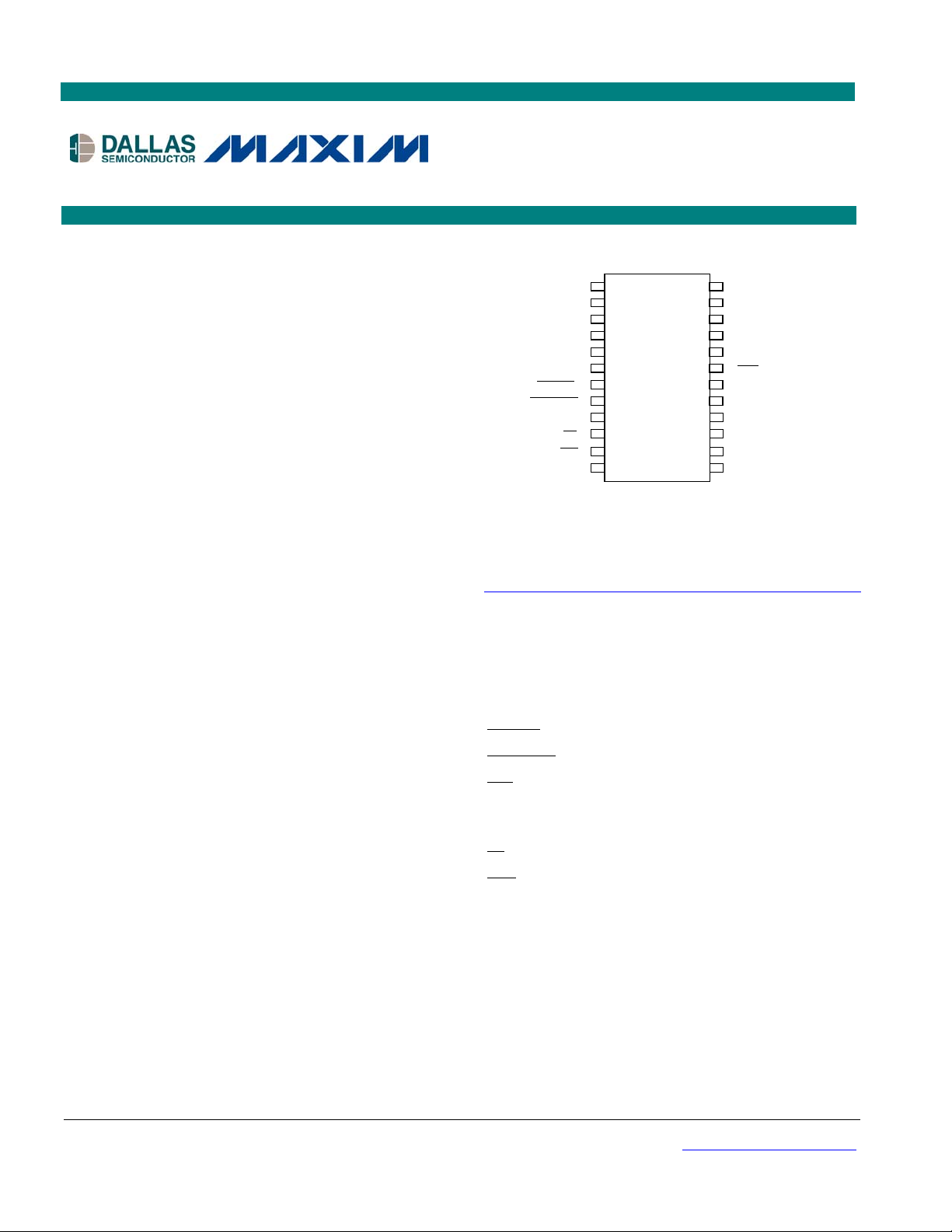
PIN ASSIGNMENT (Top View)
V
BAT
X1
X2
GND
N.C.
COMSEL
INSPEC
OUTSPEC
N.C.
ST
INT
GND
1
2
3
4
5
6
7
8
9
10
11
12
DS1616 24 DIP (600mil)
DS1616S 24 SO (300mil)
Package Dimension Information
http://www.maxim-ic.com/TechSupport/DallasPackInfo.htm
24
23
22
21
20
19
18
17
16
15
14
13
V
CC
Rx
Tx
SCLK
I/O
RST
GND
GND
IN3
IN2
IN1
N.C.
PIN DESCRIPTION
V
BAT
X1 - Crystal Input
X2 - Crystal Output
AINx - Analog in
INSPEC - In-Specification Output
OUTSPEC - Out-of-Specification Output
INT - Interrupt Output
GND - Digital Ground
AGND - Analog Ground
ST - Start/Status Input
RST - 3-Wire Reset Input
I/O - 3-Wire Input/Output
SCLK - 3-Wire Clock Input
Tx - Transmit Output
Rx - Receive Input
COMSEL - Communication Select
V
CC
- Battery Supply
- +5V Supply
Note: Some revisions of this device may incorporate deviations from published specifications known as errata. Multiple revisions of any device
may be simultaneously available through various sales channels. For information about device errata, click here: http://www.maxim-ic.com/errata.
1 of 28 081902
Page 2

DS1616
ORDERING INFORMATION
PART PIN-PACKAGE TEMP RANGE
DS1616 24 DIP -40°C to +85°C
DS1616S 24 SO 0°C to +70°C
DESCRIPTION
The DS1616 is an integrated temperature/data recorder. It combines a real-time clock (RTC),
temperature sensor, and a three input muxed 8-bit Analog-to-Digital Converter (ADC). Data logging is
supported for all four data channels and the and histogram functionality is supported for the temperature
sensor and ADC Channel 1 only. A programmable sample rate feature makes the device ideal for
applications requiring datalogging over short or long time frames.
The RTC provides seconds, minutes, hours, day, date, month, and year information with leap year
compensation, Year 2000 compliance, and also provides an alarm interrupt. Temperature measurement is
provided via integrated thermal technology which can measure temperatures from -40°C to +85°C in
0.5°C increments. An integrated three input muxed 8-bit ADC allows the device to record data from
other types of sensors.
The datalog function samples data at a user-defined sample rate and writes the data to the Datalog
memory. A total of 2048 bytes of data may be recorded. If only one data channel is selected, a total of
2048 samples can be recorded for that channel. If two channels are enabled, each channel can record
1024 samples. If three or four channels are enabled, each channel can record 512 samples. In the case of
only three channels enabled, the location corresponding to the disabled channel will be 0 to allow the rollover function to work smoothly.
Histogram functionality is provided for the Thermal Sensor and ADC Channel 1, and is implemented by
sampling the data and then incrementing the count value in a data bin associated with that value. The
DS1616 provides 63 2-byte data bins in 2°C increments for the temperature channel and 64 2-byte data
bins in 4-bit resolution steps (32mV/bin) for the ADC Data Channel 1. The sampling rate can be
programmed at intervals ranging from once per minute to once every 255 minutes.
The DS1616 provides programmable high- and low-temperature alarm trip points that allow the device to
monitor whether the temperature stays within desired limits. Likewise, high- and low- trip points can be
programmed for the ADC data. The device can drive an interrupt or status pin if the ADC data falls
outside of the programmable limits. The Temperature Sensor and Channel 1 of the ADC can also have
any event that falls outside of the programmed limits recorded with a time and date stamp and the
duration of the out-of-limits condition for additional analysis in the Alarm Memory. The DS1616 can be
programmed to begin sampling data via a pushbutton input or via a command sent over the serial
interface by a host machine.
A 64-bit serial number is available for unique product identification and tracking.
OVERVIEW
The block diagram in Figure 1 shows the relationship between the major control and memory sections of
the DS1616. The device has six major data components: 1) RTC and control blocks, 2) 32-byte User NV
RAM with 64-bit lasered serial number, 3) 96 bytes of alarm event/duration memory, 4) 128 bytes of
temperature histogram RAM, 5) 128 bytes of ADC Channel 1 data histogram RAM, and 6) 2048 bytes of
datalog memory. All memory is arranged in a single linear address space.
2 of 28
Page 3
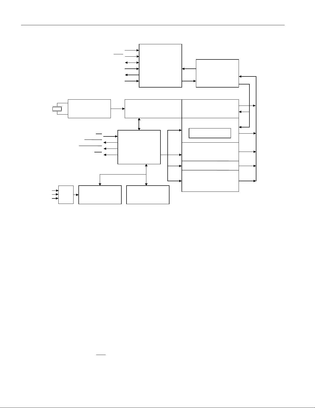
DS1616 Block Diagram Figure 1
SCLK
RST
I/O
COMSEL
Tx
Rx
X1
OSCILLATOR
AND
X2
DIVIDER
ST
INSPEC
OUTSPEC
INT
INTERNAL RTC
AND CONTROL
REGISTERS
CONTROL
LOGIC
SERIAL
INTER FACE
DS1616
MEMORY
FUNCTION
CONTROL
RTC AND CONTROL
REGISTERS
USER NVRAM
OPTIONAL
SERIAL NUMBER
ALARM TIME STAMP
AND DURATION
LOGGING MEMORY
HISTOGRAM MEMORY
DATALOG MEMORY
AIN
3 TO 1
MUX
A/D
CONVERTER
TEMPERATURE
SENSOR
SIGNAL DESCRIPTIONS
The following paragraphs describe the function of each pin.
VCC - VCC is a +5-volt input supply. Communication with the DS1616 can take place only when VCC is
connected to a +5-volt supply.
- Battery input for standard lithium cell or other energy source. All functions of the DS1616 with the
V
bat
exception of the serial interface circuitry are powered by V
powered by V
when VCC > V
CC
. If a battery or other energy source is not used, V
bat
connected directly to GND.
GND - GND connections are not internally connected, so all GND connections must be connected
directly to ground.
AGND - Analog ground should be connected directly to digital ground externally to eliminate ground
noise and potential differences.
when VCC < V
bat
. All functions are
bat
should be
bat
COMSEL (Communication Select Input) - This pin determines whether serial communication is
asynchronous or synchronous. When pulled high to V
place via the SCLK, I/O, and
RST pins. When COMSEL is tied to ground, asynchronous communication
, communication is synchronous and will take
CC
utilizing the TX and RX pins is selected. If this pin is floated, the DS1616 will operate in the
asynchronous communications mode since the COMSEL pin has a weak internal pulldown resistor.
3 of 28
Page 4

DS1616
Tx (Transmit Output) - Transmit output of the asynchronous serial interface. Tx is tri-stated whenever
VCC < V
bat
.
Rx (Receive Input) - Receive input of the asynchronous serial interface.
SCLK (3-Wire Serial Clock Input) - The SCLK pin is the serial clock input for the 3-wire synchronous
communications channel.
I/O (3-Wire Input/Output) - The I/O pin is the data Input/Output signal for the 3-wire synchronous
communications channel.
RST (3-Wire Reset Input) - The RST pin is the communications reset pin for the 3-wire synchronous
communications channel.
NTI (Interrupt Output) - The INT pin is an open drain active low output that can be connected to an
interrupt input of a microprocessor. The
INT output remains low as long as the status bit causing the
interrupt is present and the corresponding interrupt-enable bit is set.
INSPEC (Open Drain In-Specification Output) - This pin, in conjunction with the OUTSPEC pin, is
used to signal the status of the operation and data of the DS1616.
OUTSPEC (Open Drain Out-of-Specification Output) - This pin, in conjunction with the INSPEC pin,
is used to signal the status of the operation and data of the DS1616.
ST (Start/Status Button Input) - The ST pin provides two functions. First, when enabled as the datalog
start source (SE bit in Control 1 register is a logic 1), the ST pin is used to instruct the DS1616 to begin
recording data based on the programmed start delay and data sample rate. The ST pin must be held low
for at least 0.5 seconds for a datalog mission to begin.
Secondly, the ST pin can be used to poll the status of the recorded data. After datalogging has begun, the
ST pin instructs the DS1616 to report the status of the recorded data via the INSPEC and OUTSPEC pins.
AIN1, AIN2, AIN3 (Analog Inputs) - The AINx pins are the muxed inputs to the ADC.
X1, X2 - Connections for a standard 32.768 kHz quartz crystal, Daiwa part number DT-26S or
equivalent. For greatest accuracy, the DS1616 must be used with a crystal that has a specified load
capacitance of 6 pF. There is no need for external capacitors or resistors. Note: X1 and X2 are very high
impedance nodes. It is recommended that they and the crystal be guard-ringed with ground and that high
frequency signals be kept away from the crystal area. For more information on crystal selection and
crystal layout considerations, refer to Application Note 58: Crystal Considerations with Dallas Real-Time
Clocks.
N.C. (No Connect) - These pins should be left unconnected or tied to ground.
4 of 28
Page 5

DS1616
MEMORY
The memory map in Figure 2a shows the general organization of the DS1616. As can be seen in the
figure, the device is segmented into 32-byte pages. Pages 0 and 1 contain the RTC and Control registers
(see Figure 2b for more detail). The User NV RAM resides in page 2. Pages 17 to 19 are assigned to
storing the alarm time stamps and durations and pages 64 to 71 are reserved for histogram memory. The
data logging memory covers pages 128 to 191. Memory pages 3 to 16, 20 to 63, 68 to 127, and 192 and
up are reserved for future extensions.
The end user can write only to the RTC and Control registers and the User NV RAM. The rest of the
memory map is read-only from the end user’s perspective.
DS1616 MEMORY MAP Figure 2a
Address Register definition Page(s)
0000H
003FH
0040H
005FH
0060H
0217H
0218H
021FH
0220H
027FH
0280H
07FFH
0800H
087FH
0880H
08FFH
0900H
0FFFH
1000H
17FFH
1800H
and higher
RTC and Control Registers 0 - 1
User NV RAM 2
(Reserved for Future Extensions) 3 – 16*
Serial Number 16**
Alarm Time Stamps and Durations 17 – 19
(Reserved for Future Extensions) 20 – 63
Temperature Histogram (63 Bins of 2 Bytes Each) 64 – 67
ADC Channel 1 Data Histogram (64 Bins of 2 Bytes Each) 68 – 71
(Reserved for Future Extensions) 72 – 127
Datalog Memory (64 pages) 128 – 191
(Reserved for Future Extensions) 192 +
* First 8 bytes
** Last 8 bytes
5 of 28
Page 6
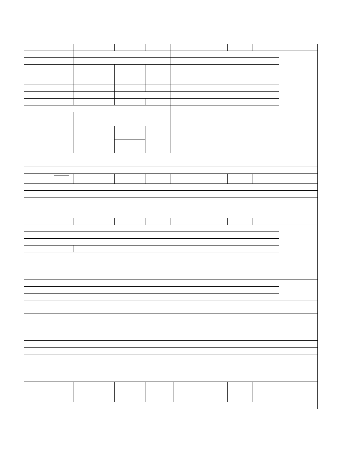
DS1616 RTC AND CONTROL PAGE Figure 2b
Addr. Bit 7 Bit 6 Bit 5 Bit 4 Bit 3 Bit 2 Bit 1 Bit 0 Function
00 0 10 Seconds Single Seconds
01 0 10 Minutes Single Minutes
10 h02 0 12/24
A/P
030 0 000 Day Of Week
04 0 0 10 Date Single Date
05 Y2K 0 0 10 m. Single Months
06 10 Years Single Years
07 MS 10 Seconds Alarm Single Seconds Alarm
08 MM 10 Minutes Alarm Single Minutes Alarm
10 ha.09 MH 12/24
A/P
0A MD 0 0 0 0 Day Of Week Alarm
0B Low Temperature Threshold
0C High Temperature Threshold
0D Number Of Minutes Between Temperature Conversions Sample Rate
0E
0F (reads 00h) Reserved
10 (reads 00h) Reserved
11 Current Temperature Temperature
12 Start Delay Register (LSB) Start Delay
13 Start Delay Register (MSB) Start Delay
14 DR MEM CLR MIP SIP LOBAT TLF THF ALMF Status 1
15 Minutes
16 Hours
17 Date
18 Y2K Month
19 Year
1A Low Byte
1B Medium Byte
1C High Byte
1D Low Byte
1E Medium Byte
1F High Byte
20 Current ADC Channel 1 Data Sensor Input
21 Current ADC Channel 2 Data Sensor Input
22 Current ADC Channel 3 Data Sensor Input
23 Low ADC Channel 1 Data Threshold ADC Data
24 High ADC Channel 1 Data Threshold Ch1 Alarm
25 Low ADC Channel 2 Data Threshold ADC Data
26 High ADC Channel 2 Data Threshold Ch2 Alarm
27 Low ADC Channel 3 Data Threshold ADC Data
28 High ADC Channel 3 Data Threshold Ch3 Alarm
29 0 CS0
2A 0 ALF1 AHF1 ALF2 AHF2 ALF3 AHF3 0 Status 2
2B-3F (reads 00h) Reserved
EOSC
CLR 0 SE RO TLIE THIE AIE Control 1
CS1
(Temp)
(ADC 1)
10 h Single Hours
10 h.
alm.
CS2
(ADC 2)
CS3
(ADC 3)
Single Hours Alarm
ALIE AHIE 0 Control 2
RealTime
Clock
Registers
RealTime
Clock
Alarm
Temperature
Alarm
Start
Time
Stamp
Current
Samples
Counter
Total
Samples
Counter
DS1616
1
2
3
6 of 28
Page 7
DS1616 ALARM TIME STAMPS AND DURATIONS FOR THE THERMAL
SENSOR AND ADC CHANNEL 1 Figure 2c
Sample Counter Address
(Low, Medium, High Bytes)
220, 221, 222 223 T1 Low
224, 225, 226 227 T2 Low
228, 229, 22A 22B T3 Low
22C, 22D, 22E 22F T4 Low
230, 231, 232 233 T5 Low
234, 235, 236 237 T6 Low
238, 239, 23A 23B T1 High
23C, 23D, 23E 23F T2 High
240, 241, 242 243 T3 High
244, 245, 246 247 T4 High
248, 249, 24A 24B T5 High
24C, 24D, 24E 24F T6 High
250, 251, 252 253 D1 Low
254, 255, 256 257 D2 Low
258, 259, 25A 25B D3 Low
25C, 25D, 25E 25F D4 Low
260, 261, 262 263 D5 Low
264, 265, 266 267 D6 Low
268, 269, 26A 26B D1 High
26C, 26D, 26E 26F D2 High
270, 271, 272 273 D3 High
274, 275, 276 277 D4 High
278, 279, 27A 27B D6 High
27C, 27D, 27E 27F D6 High
Duration
Address
Register
DS1616
DS1616 TEMPERATURE HISTOGRAM DATA BINS Figure 2d
Address (Low – High Byte) Register
800 – 801 -40, -39.5, -39, -38.5°C Data Bin
802 – 803 -38, -37.5, -37, -36.5°C Data Bin
804
↓
87B
87C – 87D 84, 84.5, 85°C Data Bin
↓
DS1616 ADC DATA HISTOGRAM DATA BINS Figure 2e
Address (Low – High Byte) Register
880 – 881 Channel 1 Code 00, 01, 02, 03h Data Bin
882 – 883 Channel 1 Code 04, 05, 06, 07h Data Bin
884
↓
8FD
8FE – 8FF Channel 1 Code FC, FD, FE, FFh Data Bin
↓
THERMAL SENSOR
The key to temperature monitoring in the DS1616 is an integrated thermal sensor. The thermal sensor
can measure temperature from -40°C to +85°C in 0.5°C increments (Fahrenheit equivalent is -40°F to
+183.2°F in 1.8°F increments). The thermal sensor provides an accuracy of ±2°C.
7 of 28
Page 8

DS1616
The thermal sensor is enabled by setting the CS0 bit of the Control 2 register to a logic 1. If the CS0 bit
is a logic 0, the thermal sensor will not be activated during a datalogging mission or for an individual
Read Data command. If CS0 = 0, the value in the Current Temperature register will be 11111111b.
The format of temperature data is defined such that the temperature value is maintained in a single byte of
data. Table 1 illustrates the format of the temperature data byte format. The values of T[7..0] range from
00000000b (for -40°C) to 11111010b (for +85°C). Each increment in the value of T[7..0] represents an
increase in temperature of 0.5°C. The following formula can be used to translate the temperature data
byte value into degrees Celsius: °C = 0.5(T[7..0]) - 40
TEMPERATURE DATA BYTE FORMAT Table 1
MSb LSb
T7 T6 T5 T4 T3 T2 T1 T0
When a datalog mission has been initiated and the thermal sensor is enabled (CS0=1), the DS1616
provides temperature recording at regular intervals. However, the device also allows for immediate
temperature sensing upon a user’s command when the device is not currently on a datalog mission and
the thermal sensor is enabled (CS0=1). This is accomplished by issuing the Read Data command to the
DS1616 over the serial interface.
The most recently recorded temperature value is written to the Current Temperature register, regardless of
whether that value was recorded from a datalog mission or from the issuance of the Read Data command.
The status of the contents of this register is provided by the Data Ready (DR) bit in the Status 1 register.
If DR is a logic 1, the data is valid. If DR is a logic 0, the data may not be reliable. If CS0 in the Control
2 register is a 0 such that the thermal sensor is disabled, the value in the Current Temperature register will
be 11111111b. The Read Data command will not output this byte of data.
During a datalog mission, the DR bit is cleared to a logic 0 when a temperature conversion has been
initiated and is set to a logic 1 upon the completion of the conversion. Likewise, the DR bit is cleared
immediately after the Read Data command is issued and is set to a logic 1 upon the completion of the
conversion. The Read Data command will only read the values in the current temperature/ADC data that
have been enabled by the CSx[03] bits in the control 2 register.
ANALOG-TO-DIGITAL CONVERTER (ADC)
The DS1616 contains an integrated 8-bit ADC with a 3 to 1 input mux to allow multiple sensors to be
monitored. An on-chip voltage reference is also provided by an integrated band gap circuit (2.04V ±3%).
The ADC input voltage must not be greater than the battery voltage.
An analog-to-digital conversion is the process of assigning a digital value to an analog input voltage.
This code represents the input value as a fraction of the full scale voltage (FSV) range. Thus the FSV
range is then divided by the ADC into 256 codes (8 bits). The FSV range is bounded by an upper limit
equal to the reference voltage and the lower limit, which is ground. The 2.04V (typical) bandgap
reference provides a resolution of 8mV between codes.
An input voltage equal to the reference voltage converts to FFh while an input voltage equal to ground
converts to 00h. The relative linearity of the ADC is ±0.5 LSB.
When a datalog mission has been initiated and one or more of the Analog Inputs are enabled (CS[1-3] =
1), the DS1616 provides data conversion and recording at regular intervals. However, the device also
8 of 28
Page 9

DS1616
allows for immediate data conversion upon a user’s command when the device is not currently
performing a conversion and one or more of the Analog Inputs are enabled (CS[1-3] = 1). This is
accomplished by issuing the Read Data command to the DS1616 over the serial interface.
The most recently recorded data value is written to the Current Data register that corresponds to the
analog channel(s) that is(are) enabled, regardless of whether that value was recorded from a datalog
mission or from the issuance of the Read Data command. The status of the contents of this register is
provided by the Data Ready (DR) bit in the Status 1 register. If DR is a logic 1, the data is valid. If DR is
a logic 0, the data may not be reliable. If a channel is not enabled, CS[1-3] is a logic 0, the contents of
the corresponding Current Data register will be 00000000b and not outputted when a Read Data
command is issued.
During a datalog mission, the DR bit is cleared to a logic 0 when a data conversion has been initiated and
is set to a logic 1 upon the completion of the conversion. Likewise, the DR bit is cleared immediately
after the Read Data command is issued and is set to a logic 1 upon the completion of the conversion.
DATA LOGGING
When the DS1616 datalogging function is enabled, the device is said to be on a “datalog mission” until
the datalogging is stopped.
During a datalog mission, temperature and/or ADC samples are successively written to the Datalog
memory pages. These memory pages are located at addresses 1000h to 17FFh.
The end user can program the DS1616 to record data from all four data channels or just one channel.
Channel selection is determined by the setting the Channel Select bits (CS0, CS1, CS2 and CS3) in the
Control 2 register to the appropriate states. A 1 in the CSx bit will enable the channel and allow the
results to be reported, while a 0 will disable the channel, prevent its data from being recorded, prevent the
data from being reported by the Read Data command, and set the contents of the memory location for the
Current Data register corresponding to that channel to a constant value, all 1s for the thermal sensor or all
0s for the ADC channels.
When 3 or 4 data channels are selected, the first data sample is written to address location 1000h, the
second is written to address location 1001h. The address is incremented with each additional data
sample, with samples alternating between the enabled channels. The second sample is always measured
immediately after the completion of the first measurement with the third and forth samples following the
second. The order of the sampling is the same as the order of the Channel Select registers. CS0 will be
sampled first, if it is enabled, followed by CS1, CS2 and CS3 if they are enabled. Any disabled channels
will be skipped. A total of 2048 registers have been reserved for datalog data, providing a total of 512
samples for each channel.
When three out of the four channels are enabled, a fourth byte of all 0s will be recorded in the Datalog
Memory after the three bytes of data from the enabled channels in order to allow the data to rollover and
remain in the correct positions.
When two data channels are selected, the first data sample is written to address location 1000h and the
second is then written to address location 1001h. The address is incremented with each additional data
sample, with samples alternating between the enabled channels.
The second sample is always measured immediately after the completion of the first measurement. A
total of 2048 registers have been reserved for datalog data, providing a total of 1024 samples each
channel.
9 of 28
Page 10

DS1616
If one data channel is selected, the entire datalog memory is dedicated to that one channel and therefore a
total of 2048 samples can be recorded.
A datalog mission can be initiated via two different methods: by a host instruction over the serial
interface or by a pushbutton input. When the SE bit in the Control 1 register is cleared to a logic 0, the
start function of the ST pin is disabled and writing any non-0 value to the Sample Rate register will start a
mission. When the SE bit is set to a logic 1, the pushbutton method of starting a mission is enabled.
Under this mode of operation, the DS1616 will begin a datalog mission when a non-0 value has been
written to the Sample Rate register and the ST pin has been held low for at least 0.5 seconds.
The sample rate during a datalog mission is equal to the value written to the Sample Rate register
multiplied by one minute. Writing a 0 to the MIP bit in the Status 1 register completes the mission.
Upon initiation of datalog mission by either method, the DS1616 will do two things:
1. The
INSPEC and OUTSPEC pins will generate four low pulses simultaneously.
2. The Mission-in-Progress (MIP) bit in the Status 1 register is set to a 1.
The time at which the first datalog sample is measured is dependent upon the value in the Start Delay
registers. The two-byte Start Delay register provide a method for the end user to program a delay before
sampling commences. The delay is roughly equal to the value in the Start Delay register times one
minute. For example, if the Start Delay register contain a value of 10, then the device will begin
recording data approximately ten minutes after it received either the pushbutton start signal or start
instruction. The Start Delay register are located at addresses 0012h and 0013h, with register 0012h being
the LSB and register 0013h being the MSB. The Start Delay register decrements every time the Seconds
register rolls over from 59 to 00. When this Start Delay register contains a 00, the first datalog sample
will be taken when the seconds register rolls over from 59 to 00.
The user has two options for dealing with the potential occurrence of a data overrun (i.e., more than 2048
total data samples). The first option is to enable the rollover feature of the DS1616. This is accomplished
by setting the Rollover bit (bit 3 of the Control 1 register) to 1. When the Rollover feature is enabled,
new data is written over previous data, starting with address 1000h. For example, if the Datalog memory
has been completely filled (i.e., 2048 data samples have been recorded) the next data sample will be
written to address location 1000h and the address pointer will be incremented with each successive data
sample.
The second option for dealing with data overrun is to stop recording data after the datalog memory has
been completely used. In other words, the DS1616 will stop recording data values after 2048 data
samples. This feature is enabled by disabling the Rollover feature. (Bit 3 of the Control 1 Register) set to
0.
It should be noted that during a datalog mission, a time stamp for the first sample is recorded, but is not
included for each subsequent sample. However, the time of acquisition for any data sample is easily
determined by considering the start time, the sample rate, the value in the Current Sample Counter, and
the address of the particular data sample in the datalog memory. If no rollover has occurred in the
datalog memory, the sample time associated with any particular data point can be calculated by
multiplying the address of the data by the sample rate and adding that to the stored start time value.
If the rollover feature has been enabled, the user can determine if rollover has occurred by reading the
value in the Current Samples register. This register counts the total number of samples that have been
acquired. If this value is greater than 07FFh (decimal 2047) then the user knows that rollover has
10 of 28
Page 11

DS1616
occurred. If rollover has occurred, the user needs to determine how many times rollover occurred in
determining the sample time for any particular data sample.
As a safety measure, the DS1616 has been designed such that the end user cannot write to the Datalog
Memory. This prevents the falsification of datalog data by writing values to datalog registers.
DATA HISTOGRAM
While on a datalog mission, the DS1616 also records a histogram of the temperature and/or ADC
Channel 1 data. The temperature histogram is provided by a series of 63 2-byte “data bins” that are
located in the Temperature Histogram memory pages (addresses 0800h to 087Fh). Each bin consists of a
16-bit binary counter that is incremented each time an acquired temperature value falls into the range of
the bin. The least significant byte of each bin is stored at the lower address. Bin 0 begins at memory
address 0800h, bin 1 at 0802h, and so on up to 087Ch for bin 62. See Figure 2d for temperature
histogram address map.
Likewise, the ADC Channel 1Data histogram is provided by a series of 64 2-byte “data bins” that are
located in the ADC Data Histogram memory pages (addresses 0880h to 08FFh). Each data bin represents
four ADC codes (32mV/bin). For example, bin 0 counts the frequency of ADC codes from 00-03h. Bin
1 counts the frequency of ADC codes from 04-07h, and so on. See Figure 2e for ADC Data histogram
address map.
After a temperature and/or ADC conversion is completed, the number of the bin to be updated is
determined by dropping the two least significant bits of the binary data value. For example, bin 0 of the
temperature histogram will be updated with every temperature reading from -40°C to -38.5°C. In the
same way, bin 1 is associated with the range of -38°C to -36.5°C. Bin 62, finally, counts temperature
values in the range of +84°C to +85.0°C. Since the device will not generate temperature values higher
than 85.0°C, bin 62 covers only three temperature values. The memory for a potential 64th bin exists, but
will always read 0s.
Since each data bin contains 2 bytes, a total of 65,535 samples can be accumulated. If more samples are
measured, the data bin will remain at the maximum value. In other words, the data bin value will not rollover in the event of an overrun.
ALARM LOGGING
For some applications it may be essential to record exactly when a data sample exceeds a predefined
tolerance band and for how long the violation remained. The Thermal Sensor (CS1) and ADC Channel 1
(CS2) are equipped with the alarm logging feature. The ADC Channels 2 & 3 do not have the logging
feature, but they still have the alarm feature and the ability to trigger an interrupt. If an out of tolerance
condition occurs on channels 2 or 3, the time and duration can be calculated from the Memory if the
memory has not rolled over since the alarm.
A tolerance band is specified by means of the Temperature Alarm registers (addresses 000Bh and 000Ch)
and the ADC Data Alarm [1-3] registers (addresses 0024h to 0029h). See figure 2b for more details on
the memory mapping. One can set a high and a low threshold. As long as the data samples stay within
the tolerance bands (i.e., are higher than the low threshold and lower than the high threshold), the DS1616
will not record any alarm.
If the temperature violates the temperature band, the DS1616 will generate an alarm and set either the
Temperature-High Flag (THF) or the Temperature-Low Flag (TLF) in the Status 1 register (address
0014h). In addition, the device generates a time stamp of when the alarm occurred and records the
11 of 28
Page 12

DS1616
duration of the alarming condition. The INT pin will be asserted by a high temperature alarm if the
Temperature-High Interrupt Enable (THIE) is set and will be asserted by a low temperature alarm if the
Temperature-Low Interrupt Enable (TLIE) is set.
Likewise, if ADC Channel 1 Data measurement violates the ADC Data band, either the ADC Data-High
1 or Data-Low 1 Flag (AHF1 or ALF1) will be set, a time stamp will be generated, and the duration of the
violation will be recorded. The INT pin will be asserted by a high-alarm if the ADC Data-High Interrupt
Enable (AHIE) is set and will be asserted by a low-alarm if the ADC Data-Low Interrupt Enable (ALIE)
is set.
The device stores a time stamp of a violating condition by copying contents of the 3-byte Current
Samples Counter when the alarm occurred. The least significant byte is stored at the lower address. One
address higher than a time stamp, the DS1616 maintains a 1-byte duration counter that stores the number
of times the data was found to be beyond the threshold. If this counter has reached its limit after 255
consecutive data readings and the data has not yet returned to a level within the tolerance band, the device
will issue another time stamp at the next higher address and open another counter to record the duration.
If the data returns to normal before the counter has reached its limit, the duration counter of the particular
time stamp will not increment any further. Should the data again cross this threshold, new time stamp will
be recorded and its associated counter will increment with each data reading outside the tolerance band.
This algorithm is implemented for the low- as well as for the high- thresholds.
Time stamps and durations for low-temperature violations are stored in the Registers 0220h to 0237h
(24 bytes) and registers 0238h to 024Fh (24 bytes) are reserved for high-temperature violations.
Registers 0250h to 0267h are reserved for low-ADC Channel 1 Data violations and registers 0268h to
027Fh are reserved for high-ADC Channel 1 Data violations.
This allocation allows the recording of 24 individual alarm events and periods (six each for hightemperature, low-temperature, high-ADC Channel 1 Data, and low-ADC Channel 1 Data violations).
The date and time of each of these periods can be determined from the Start Time Stamp and the time
sample rate. Figure 2c illustrates the Alarm Time Stamps and Durations registers.
INSPEC AND OUTSPEC PINS
Two special output pins, INSPEC and OUTSPEC , are intended to output the status of the DS1616. More
specifically, these pins can be used to control the illumination of LEDs. For example, the
INSPEC pin can
be used to pulse a green LED and the OUTSPEC pin can be used to pulse a red LED. When the end user
starts a datalog mission or polls the device for information, one or both of these pins will be pulsed four
times. Depending on the status of the device, both pins will be pulsed simultaneously or just one pin will
be pulsed at a time. Each pulse is 62.5 ms in duration and will start every half second. See Figures 9 and
10 for further details.
12 of 28
Page 13

DS1616
The INSPEC and OUTSPEC pins are used to provide visual feedback to the end user in the following
situations:
1. Datalog Mission Start
When a datalog mission is first initiated, the INSPEC and OUTSPEC pins will generate four low pulses
simultaneously to give the end user a visual indication that a datalog mission has begun.
2. Request for Status of Data
Following a user request for the status of recorded data, the INSPEC pin will generate four low pulses if
the recorded data is within the user-defined limits (as set in the Threshold registers). If the recorded
temperature data contains any readings that fall outside of these high- and low-temperature thresholds or
if the recorded ADC data from any of the three ADC channels that are enabled contains any readings that
fall outside of these high- and low-ADC Channel [1-3] Data thresholds, the OUTSPEC pin will be pulsed
four times. If the request comes after the mission has started (i.e., MIP = 1), but before the first sample
has been recorded, the INSPEC and OUTSPEC pins will generate a total of four low pulses alternately,
starting with the OUTSPEC pin.
The DS1616 provides two methods for the user to request the status of the data. The first method is to
send the Specification Test command over the serial interface. The second method is by holding the ST
pin low for at least half a second after the datalogger has already been started.
CLOCK, CALENDAR, AND ALARM
The time and calendar information is accessed by reading/writing the appropriate register bytes. Note
that some bits are set to 0. These bits will always read 0 regardless of how they are written. The contents
of the time, calendar, and alarm registers are in the Binary-Coded Decimal (BCD) format and Year 2000
compliant.
The RTC can be read at any time and the values used in other parts of the system outside the data logger
by issuing a Read Page command for memory page 0. See figure 2C for more details on the RTC
memory map.
The DS1616 can run in either 12-hour or 24-hour mode. Bit 6 of the hours register is defined as the 12or 24-hour mode select bit. When high, the 12-hour mode is selected. In the 12-hour mode, bit 5 is the
AM/PM bit with logic 1 being PM. In the 24-hour mode, bit 5 is the second 10-hour bit (20-23 hours).
The DS1616 also contains a time of day alarm. The alarm registers are located in registers 0007h to
000Ah. Bit 7 of each of the alarm registers are mask bits (see Table 2). When all of the mask bits are
logic 0, an alarm will occur once per week when the values stored in timekeeping registers 0000h to
0003h match the values stored in the time of day alarm registers. An alarm will be generated every day
when mask bit of the day alarm register is set to 1. An alarm will be generated every hour when the day
and hour alarm mask bits are set to 1. Similarly, an alarm will be generated every minute when the day,
hour, and minute alarm mask bits are set to 1. When day, hour, minute, and seconds alarm mask bits are
set to 1, an alarm will occur every second.
As a security measure to prevent unauthorized tampering, changing any value in the RTC and Control
registers (with the exception of the Status registers) will stop a datalog mission and clear the Mission-inProgress (MIP) bit.
13 of 28
Page 14

TIME OF DAY ALARM BITS Table 2
ALARM REGISTER MASK BITS (bit 7)
SECONDSMSMINUTES
MM
1 1 1 1 ALARM ONCE PER SECOND
0 1 1 1 ALARM WHEN SECONDS MATCH
0 0 1 1 ALARM WHEN MINUTES AND SECONDS MATCH
0 0 0 1 ALARM WHEN HOURS, MINUTES, AND
0 0 0 0 ALARM WHEN DAY, HOURS, MINUTES, AND
HOURSMHDAYS
MD
SECONDS MATCH
SECONDS MATCH
SPECIAL PURPOSE REGISTERS
The following description defines the operation of the special function registers of the DS1616.
CONTROL 1 REGISTER
MSb LSb
EOSC
CLR 0 SE RO TLIE THIE AIE
DS1616
EOSC - Enable oscillator - This bit controls the state of the oscillator in battery back-up mode only.
When set to logic 0, the oscillator is active. When this bit is set to a logic 1, the oscillator is stopped and
the DS1616 is placed into a low-power standby mode with a current drain of less than 100 nanoamps at
room temperature. When Vcc is applied or when MIP =1, the oscillator is active regardless of the state of
this bit.
CLR - Clear Enable - This bit enables the Clear Memory command. When this bit is set to a 1 and the
Clear Memory command is subsequently issued, the datalog, histogram, Temperature Alarm, Current
Samples, Start Time Stamp, Start Delay, Sample Rate register, and ADC Data Alarm are all cleared to 0.
Following the issuing of the Clear Memory command, the CLR bit is also cleared to 0. If the Clear
Enable bit is set, but a command other than the Clear Memory command is issued next, the CLR bit is
cleared to a 0 and the contents of the datalog, histogram, temperature alarms, Current Samples registers,
Start Delay, Sample Rate, and ADC Data alarm register are unchanged.
SE - Start Enable - This bit enables the “start” function of the ST input. When SE is a logic 1, the ST
input is enabled as the start pin for datalogging operation. When enabled, datalogging operation begins
when the Sample Rate register contains a non-0 value AND the
ST pin has been held low for at least
0.5 seconds. When SE is a logic 0, writing any non-0 value to the Sample Rate register will start
datalogging operation.
Once datalog operation has been initiated, the first data sample occurs after the specified delay written to
the Start Delay register has elapsed.
RO - Roll-Over - This bit determines whether the datalog function of the DS1616 rolls over or stops
writing data to the datalog memory in the event that the datalog memory is completely filled. If RO is set
to a 1, the datalog memory will “roll over” after all 2048 registers in the datalog memory have been used.
In other words, after the 2048
th
register is written, the following sample will be written to register 0000,
overwriting the original data. Likewise, subsequent samples will increment through the datalog registers,
overwriting their data.
14 of 28
Page 15

DS1616
If RO is cleared to a 0, no further data samples will be written to the datalog memory after all datalog
memory registers have been filled. Samples, however, will continue to be taken and the appropriate
histogram registers will be incremented with each sample. Likewise, the temperature and ADC Data
alarms will also continue to function.
TLIE - Temperature Low Interrupt Enable - When set to a logic 1, this bit permits the Temperature Low
Flag (TLF) in the Status 1 register to assert
not initiate the
INT signal.
INT . When the TLIE bit is set to logic 0, the TLF bit does
THIE - Temperature High Interrupt Enable - When set to a logic 1, this bit permits the Temperature High
Flag (THF) in the Status 1 register to assert
not initiate the
INT signal.
INT . When the THIE bit is set to logic 0, the THF bit does
AIE - Alarm Interrupt Enable - When set to a logic 1, this bit permits the Alarm Flag (ALMF) in the
Status 1 register to assert
INT . When the AIE bit is set to logic 0, the ALMF bit does not initiate the INT
signal.
STATUS 1 REGISTER
MSb LSb
DR MEM
CLR
DR - Data Ready - This bit indicates the status of the data value in the Current Temperature and/or ADC
Data [1-3] registers after the Read Data command has been executed. When this bit is a logic 1, the
DS1616 has completed the measurement of all of the selected channels (CSx = 1) and has written valid
value(s) to the Current Temperature and/or Current ADC Data [1-3] registers. When this bit is a logic 0,
the measurements have not been completed. This bit is cleared to 0 when the Read Data command is
sent.
MIP SIP LOBAT TLF THF ALMF
MEM CLR - Memory Cleared - This bit indicates that the datalog memory, histogram memory,
Temperature Alarm, ADC Channel 1 Data Alarm, Current Samples, Start Time Stamp, Start Delay, and
Sample Rate registers are all cleared to 0. MEM CLR is cleared to 0 when a datalog mission is started
(i.e., MIP = 1).
MIP - Mission in Progress - This bit indicates the sampling status of the DS1616. If MIP is a logic 1, the
device is currently on a “mission” in which it is operating in the data logging mode. The MIP bit is
changed to a logic 1 immediately following 1) the writing of a non-0 value to the Sample Rate register
when the SE bit is a 0 or 2) a falling edge on the
ST pin if the Sample Rate register contains a non-0
value AND the SE bit is a 1.
If MIP is a logic 0, the DS1616 is not currently in datalogging mode. The MIP bit transitions from a
logic 1 to a logic 0 whenever datalogging is stopped. Datalogging is stopped when the DS1616 is cleared
via the clear bit and clear instruction or when any of the RTC or Control registers (with the exception of
the Status registers) are written to during a mission. The MIP bit can also be written to a logic 0 by the
end user to stop datalogging. It cannot, however, be written to a logic 1.
15 of 28
Page 16

DS1616
SIP - Sample in Progress - This bit indicates that the DS1616 is currently in the process of acquiring a
temperature and/or ADC sample. When the SIP bit is 0, a data conversion is not currently in process and
the next conversion will not begin for at least 250 ms. When the SIP bit is a 1, a data conversion is in
progress and NO registers or memory locations should be read or written. The SIP bit will be a 1 for a
maximum of 750 ms.
LOBAT - Low Battery Flag - This bit reflects the status of the backup power source connected to the
V
pin. A logic 1 for this bit indicates an exhausted lithium energy source.
BAT
TLF - Temperature Low Flag - A logic 1 in the Temperature Low Flag bit indicates that the temperature
is/has been less than or equal to the value in the Temperature Low Threshold register. If TLIE is also a
logic 1, the
INT pin will go low. TLF is cleared by writing this bit to a logic 0. The Clear Memory
command has no effect on this bit.
THF - Temperature High Flag - A logic 1 in the Temperature High Flag bit indicates that the temperature
is/has been greater than or equal to the value in the Temperature High Threshold register. If THIE is also
a logic 1, the
INT pin will go low. THF is cleared by writing this bit to a logic 0. The Clear Memory
command has no effect on this bit.
ALMF - Alarm Flag - A logic 1 in the Alarm Flag bit indicates that the current time has matched the time
of day Alarm registers. If the AIE bit is also a logic 1, the
INT pin will go low. ALMF is cleared by
writing this bit to a logic 0. The Clear Memory command has no effect on this bit.
SAMPLE RATE REGISTER
MSb LSb
SR7 SR6 SR5 SR4 SR3 SR2 SR1 SR0
The data sample rate for the DS1616 can range from once per minute to once per 255 minutes. The rate
is equal to the value written to the Sample Rate register multiplied by one minute.
This register can only be written to a new value when the MEM CLR bit in the Status 1 register is set
to 1. In other words, once a datalog mission has started, it cannot be changed without first issuing the
Clear Memory command.
The Sample Rate register is cleared by issuing the Clear Memory command.
START DELAY RESISTER
MSb LSb
D15 D14 D13 D12 D11 D10 D9 D8
D7 D6 D5 D4 D3 D2 D1 D0
The Start Delay register determines the amount of delay before the DS1616 begins to take data
measurements. The amount of the delay is roughly equal to the value in the register multiplied by one
minute. If the register contains 00h, the first sample will begin when the seconds register rolls over from
59 to 00.
16 of 28
Page 17

DS1616
The value in this register decrements each time the seconds register rolls over from 59 to 00 until the Start
Delay register reaches a value of 00h.
TEMPERATURE-HIGH THRESHOLD REGISTER
MSb LSb
TH7 TH6 TH5 TH4 TH3 TH2 TH1 TH0
This register determines the high threshold for interrupt generation from the thermal sensor. If the
temperature is greater than or equal to the value in this register, an interrupt will be activated if the
Temperature High Interrupt Enable (THIE) bit is set to a logic 1.
TEMPERATURE-LOW THRESHOLD REGISTER
MSb LSb
TL7 TL6 TL5 TL4 TL3 TL2 TL1 TL0
This register determines the low threshold for interrupt generation from the thermal sensor. If the
temperature is less than or equal to the value in this register, an interrupt will be activated if the
Temperature Low Interrupt Enable (TLIE) bit is set to a logic 1.
CURRENT TEMPERATURE REGISTER
MSb LSb
CT7 CT6 CT5 CT4 CT3 CT2 CT1 CT0
This register provides the most recently acquired temperature measurement if the CS0 bit in the Control 2
Register is set to 1. Otherwise, the value will be all 1s and will not be reported by the Read Data
command. It contains either the most recently measured sample from automatic datalogging or it
contains data that was acquired in response to a user’s instruction for an immediate temperature
measurement. When the DS1615 is not on a mission, an immediate measurement is acquired by issuing
the Read Data command with CS0 set to 1.
After issuing the Read Data command, the value in this register is valid only if the Data Ready (DR) bit
in the Status 1 register is a logic 1.
CURRENT SAMPLES COUNTER
This 3-byte register set provides the number of samples that have been logged during the current data
logging operation (also known as a “mission”). The contents of this register can be used by software to
point to the most recent data sample in the Datalog NV RAM. The data in these registers are cleared by
enabling and issuing the Clear Memory command.
TOTAL SAMPLES COUNTER
This three-byte register set provides the total number of data samples that have been logged during the
life of the product. This value cannot be written by the end user. The value in this register is maintained
as long as the lithium energy source is available.
CURRENT ADC DATA REGISTERS [1-3]
MSb LSb
CA7 CA6 CA5 CA4 CA3 CA2 CA1 CA0
17 of 28
Page 18

DS1616
These registers provide the most recently acquired ADC inputs. For the ADC channels that are enabled
with the CS[1-3] bits in the Control 2 register set to 1. Otherwise, the value in the corresponding Current
ADC Data [1-3] register will be all 0s and not reported by the Read Data command. It contains either the
most recently measured sample from automatic datalogging or it contains data that was acquired in
response to a user’s instruction for an immediate ADC conversion. When the DS1616 is not on a
mission, an immediate measurement is acquired by issuing the Read Data command with CSx set to a 1.
After issuing the Read Data command, the value in this register is valid only if the Data Ready (DR) bit
in the Status 2 register is a logic 1.
ADC DATA-HIGH THRESHOLD REGISTERS [1-3]
MSb LSb
AH7 AH6 AH5 AH4 AH3 AH2 AH1 AH0
These registers determines the high threshold for interrupt generation from the three muxed ADC inputs.
If the data is greater than or equal to the value in the corresponding register, an interrupt will be activated
if the Data High Interrupt Enable (AHIE) bit is set to a logic 1.
ADC DATA-LOW THRESHOLD REGISTERS [1-3]
MSb LSb
AL7 AL6 AL5 AL4 AL3 AL2 AL1 AL0
These registers determines the low threshold for interrupt generation from the three muxed ADC inputs.
If the data is less than or equal to the value in the corresponding register, an interrupt will be activated if
the Data Low Interrupt Enable (ALIE) bit is set to a logic 1.
CONTROL 2 REGISTER
MSb LSb
0 CS0 CS1 CS2 CS3 ALIE AHIE 0
CSx - Channel Select [0-3] - The value of these bits determines which channels are enabled. A 1 in the
CSx bit enables the channel for data collection, recording and reporting. A 0 in the CSx bit disables the
channel so data will not be taken, recorded, or reported. This causes a common problem in retrieving
data, if the CSx bit is set to 0, the datalog and histogram data will not be downloaded from the DS1616.
ALIE - ADC Data Low Interrupt Enable - When set to a logic 1, this bit permits the ADC Data Low Flag
[1-3] (ALFx[1-3]) in the Status 2 register to assert
does not initiate the
INT signal.
INT . When the ALIE bit is set to logic 0, the ALF bit
AHIE - ADC Data High Interrupt Enable - When set to a logic 1, this bit permits the ADC Data High
Flag [1-3] (AHFx[1-3]) in the Status 2 register to assert
AHF bit does not initiate the
INT signal.
INT . When the AHIE bit is set to logic 0, the
18 of 28
Page 19

DS1616
STATUS 2 REGISTER
MSb LSb
0 ALF1 AHF1 ALF2 AHF2 ALF3 AHF3 0
ALFx - ADC Data Low Flag [1-3] - A logic 1 in the ADC Data Low Flag [1-3] bits indicate that the
ADC Channel [1-3] Data from the corresponding channel is/has been less than or equal to the value in the
corresponding ADC Data Low Threshold [1-3] register. If ALIE is also a logic 1, the
low. ALFx is cleared by writing this bit to a logic 0. The Clear Memory command has no affect on this
bit.
AHFx - ADC Data High Flag [1-3] - A logic 1 in the ADC Data High Flag [1-3] bits indicate that the
corresponding ADC Channel [1-3] Data is/has been greater than or equal to the value in the
INT pin will go
corresponding ADC Data High Threshold [1-3] register. If AHIE is also a logic 1, the
INT pin will go
low. AHFx is cleared by writing this bit to a logic 0. The Clear Memory command has no effect on this
bit.
SILICON SERIAL NUMBER
A unique 64-bit lasered serial number is located in the register bank. This serial number is divided into
three parts. The first byte contains a model number to identify the device type (19h). The next six
registers contain a unique binary number. The last serial number byte contains a CRC byte used to
validate the data in the first seven serial number registers. All 8 bytes of the serial number are read-only
registers.
The DS1616 is manufactured such that no two devices will contain an identical serial number. Blocks of
numbers can be reserved by the customer. Contact Dallas Semiconductor for special ordering
information for devices with reserved blocks of serial numbers.
SECURITY
The DS1616 provides several measures to insure data integrity for the end user. These security measures
are intended to prevent third party intermediaries from tampering with the data that has been stored in the
Datalog and Histogram memory.
As a first security measure, the Datalog and Histogram memory are read-only from the perspective of the
end user. The DS1616 can write sampled data into these memory banks, but the end user cannot write
data to individual registers. This prevents an unscrupulous intermediary from writing false data to the
DS1616. The end user, however, can clear the contents of the Datalog and Histogram memory. This is
accomplished by enabling and issuing the Clear Memory command.
A second security feature lies in the fact that once the sample rate has been selected by writing to the
Sample Rate register, it cannot be changed to another value without resetting the recorded data. This
prevents gathering many data samples at a fast sample rate and then lowering the sample rate to give the
appearance that the data was recorded over a longer period of time. The Sample Rate register can only be
written to a new value if the MEM CLR bit is set to 1.
A third security feature lies in the two integrated sample counters, the Current Samples Counter and the
Total Samples Counter. These two counters can be used to guarantee that the DS1616 data has not been
cleared at any time during a given period of time. The Current Samples Counter counts the number of
samples that have occurred since the most recent data acquisition operation was started (i.e., the number
19 of 28
Page 20

DS1616
of samples since the Sample Rate register was written to a non-0 value). The Total Samples Counter
counts the total number of samples that have been recorded in the life of the device (assuming the lithium
energy source has not been removed during that time). If the end user knows the value in the Total
Samples Counter before the data acquisition operation is started, he can guarantee that the DS1616 has
not been cleared. If the Current Samples count equals the difference between the ending value and
beginning value of the Total Samples Counter, then the DS1616 data has not been cleared during that
time frame.
As a fourth security measure, changing any value in the RTC and Control registers (with the exception of
the Status registers) will stop datalogging and clear the Mission-in-Progress (MIP) bit.
SERIAL INTERFACE
The DS1616 provides two different serial communications options; asynchronous and synchronous. Both
communications options transmit the data LSb First/MSb last.
The mode of communication is selected via the COMSEL pin. When this pin is pulled high, the DS1616
operates in synchronous mode. In this mode, communication with the DS1616 is facilitated by the
SCLK, I/O, and
RST pins. When COMSEL is pulled low or floated, asynchronous communications is
selected and communication with the device occurs over the TX and RX pins. The operation of each
mode is discussed in further detail below.
Asynchronous Communication
In asynchronous mode, the DS1616 operates as a slave peripheral device which is read and written over a
half duplex asynchronous data interface at the fixed rate of 9,600 bits per second. Data is received and
transmitted in 8-bit bytes using a standard asynchronous serial communications format as shown in
Figure 3. This format is easily generated by the UART in most systems. The DS1616 data format
implements 10-bit words including 1 start bit, 8 data bits, and 1 stop bit. Data is received by the DS1616
on the RX pin and transmitted by the TX pin.
COMMUNICATION WORD FORMAT Figure 3
START
BIT
D0 D1 D2 D3 D4 D5 D6 D7
DATA
BITS
STOP
BIT
Synchronous Communication
Synchronous communication is accomplished over the 3-wire bus which is composed of three signals.
These are the
maximum data rate of 2 Mbps. All data transfers are initiated by driving the
terminated by driving
RST (reset), the SCLK (serial clock), and I/O (data I/O) pins. The 3-wire bus operates at a
RST input high and are
RST low. (See Figures 7 and 8.) A clock cycle is a sequence of a falling edge
followed by a rising edge. For data inputs, the data must be valid during the rising edge. Data bits are
output on the falling edge of the clock and remain valid through the rising edge.
When reading data from the DS1616, the I/O pin goes to a high impedance state when the clock is high.
Taking
RST low will terminate any communication and cause the I/O pin to go to a high impedance state.
20 of 28
Page 21

DS1616
General Communications Format
Communication with the DS1616 in both synchronous and asynchronous modes is accomplished by first
writing a command to the device. The command is then followed by the parameters and/or data required
by the command. The command set for the DS1616 can be seen in Table 3. Reads and writes to the
DS1616 differ in that writes are performed one byte at a time while reads are performed in page long (up
to 32-byte) bursts. Writing 1 byte at a time means that a write command has to be issued before each byte
of data that is written. For example, writing to the user NV RAM requires that the Write User NV RAM
command be written followed by the address to be written and then the actual data byte. Writing a
second data byte would require the same procedure with a new address specified. Reads, however, are
accomplished in bursts. For example, if an end user wants to read data from a specific page he would
first issue the Read Page command, followed by the address to begin reading. After the DS1616 receives
the command and starting address, it will immediately transmit the data that resides at the given address
location. However, rather than stop with that single byte of data, the DS1616 will continue transmitting
the next byte of data and will continue transmitting data until the page boundary is reached. A page read
can begin at any address, but will always end at the page boundary. Thus, a page read can range from 1
to 32 bytes. It should be noted that a read can be terminated at any time when communicating in
synchronous mode by pulling
RST to ground. However, in asynchronous mode, the DS1616 will not
stop transmitting data until the page boundary is reached.
Cyclical Redundancy Check (CRC)
When communicating in the asynchronous mode, a 16-bit CRC is transmitted by the DS1616 following
the transmission of all data. When communicating in synchronous mode, no CRC is transmitted.
The 16-bit CRC (Cyclical Redundancy Check) is used to insure the accuracy of the data that is read from
the DS1616. The CRC is generated according to the standardized CRC16-polynomial function X16 +
X15 + X2 + 1. Figure 4 illustrates the function of the generator. The CRC is generated by clearing the
CRC generator and then shifting in data from the register set being read. A 16-bit CRC is transmitted by
the DS1616 after the last register of any page of memory is read. In other words, a CRC is generated at
the end boundary of every page that is read. The CRC is transmitted starting with bit 15 and ending with
bit 0.
CRC HARDWARE DESCRIPTION AND POLYNOMIAL Figure 4
Polynomial = X16 + X15 + X2 + 1
BIT0 BIT1 BIT2 BIT3 BIT4 BIT5 BIT6 BIT7
0
X
BIT8 BIT9 XOR XOR
8
X
1
X
9
X
XOR
2
X
BIT10 BIT11 BIT12 BIT13 BIT14 BIT15
10
X
11
X
3
X
12
X
4
X
13
X
5
X
14
X
6
X
X
X
7
15
16
X
OUTPUT
CRC
21 of 28
INPUT
DATA
Page 22

DS1616
Communication Reset (Asynchronous Mode)
When transmitting the command, parameters, or data to the DS1616, it is possible that communication
might be interrupted. For example, the user might accidentally disconnect the cable linking the device to
the host computer. To insure that communication always starts at a known state when in the
asynchronous mode, the DS1616 will reset the communication if it senses a problem. This is
accomplished via two methods. First, if during the transmission of a byte of data to the DS1616, the stop
bit is not received, communication will be reset. The lack of a valid stop bit indicates that that particular
byte of data was not received correctly. Second, if more then 10-bit times expire between the reception of
1 byte of data and the reception of the next required byte, then communication will be reset.
Automatic resetting of communication is not required when communicating in the synchronous mode.
This is because of the function of the
RST pin. Pulling RST low resets the serial communication of the
DS1616.
DS1616 COMMANDS
All communication with the DS1616 is accomplished by writing a command to the device followed by
parameter byte/s if required. Table 3 illustrates the commands supported by the DS1616.
The DS1616 commands are summarized below. Note that if an invalid command is issued, no action is
taken by the device.
DS1616 COMMANDS Table 3
COMMAND FUNCTION DESCRIPTION
22h Write Byte Write 1 byte to RTC, Control registers, and User NV RAM
33h Read Page Read Page
44h Specification Test Poll status of temperature and/or ADC Data extremes
55h Read Data Instructs DS1616 to immediately measure the temperature (if
CS0 = 1) and/or perform an analog to digital conversion on the
ADC Channels Selected (if CS[1-3] = 1) and store the result in
the Current Temperature and/or Current ADC Channel [1-3]
register(s) when MIP = 0.
A5h Clear Memory This command clears the datalog, histogram, Temperature
Alarm, ADC Channel 1 Alarm, Current Samples, Start Time
Stamp, Start Delay, and Sample Rate registers when the Clear
Enable bit (CLR) in the Control 1 register is set to a 1.
1. Write Byte (22h)
Host Transmit:
D7 D6 D5 D4 D3 D2 D1 D0
00100010
0 a6a5a4a3a2a1a0
d7 d6 d5 d4 d3 d2 d1 d0
DS1616 Response: None
Note that good programming practice insists that the Clear Memory command should be issued whenever
the DS1616 is programmed to begin a new datalogging mission.
22 of 28
Page 23

DS1616
2. Read Page (33h)
Host Transmit:
D7 D6 D5 D4 D3 D2 D1 D0
00110011
a15 a14 a13 a12 a11 a10 a9 a8
a7 a6 a5 a4 a3 a2 a1 a0
DS1616 Response (Host Receives):
D7 D6 D5 D4 D3 D2 D1 D0
register a[15..0]
↓
register xxxh
Where xxx represents the last register of the page that has been accessed.
When in asynchronous mode, the TX pin becomes inactive after the last register in the page and the CRC
have been transmitted. In synchronous mode, the DS1616 will continue to transmit data as long as clocks
are presented to the serial interface. If clocks are presented after the final data bit of the last register in
the page, the DS1616 will wraparound to the first register in the page and sequentially transmit data as
long as the clocks continue.
3. Specification Test (44h)
Host Transmit:
D7 D6 D5 D4 D3 D2 D1 D0
01000100
DS1616 Response (Host Receives): Either the INSPEC or OUTSPEC pin will generate four low pulses.
Each pulse will be 62.5 ms in duration and will start every half-second.
This command instructs the DS1616 to generate four low pulses on either the
INSPEC or OUTSPEC LED
driver pins. The pin that is driven is dependent upon whether any data samples fell outside of the Highand Low-Temperature Threshold or the High- and Low-ADC Data boundaries. These pins, when used to
drive LEDs, can be used to provide a quick visual confirmation as to whether the samples remained
within the user-defined limits.
Note that the Specification test command is ignored if the
ST button is pulled to ground when the
command is issued.
4. Read Data (55h)
Host Transmit:
D7 D6 D5 D4 D3 D2 D1 D0
01010101
DS1616 Response (Host Receives): When the device is not currently data logging (i.e., MIP = 0), the
temperature and/or the analog input(s) is/are immediately converted and the value(s) is/are written to the
Current Temperature and/or Current ADC Channel [1-3] Data registers. The channels that are enabled is
determined by the CSx bits of the Control 2 Register set to 1.
The data value(s) obtained from this command is/are not stored in the datalog or histogram memory.
23 of 28
Page 24

DS1616
After this command has been executed, the user must read the Data Ready (DR) bit in the Status 1
register to determine if the measurements have been completed. If the DR bit is a logic 1, the
measurement has been completed and the value(s) in the Current Temperature and/or Current ADC
Channel [1-3] registers is/are valid. If the DR bit is a logic 0, the measurements have not been completed.
This command functions only when MIP = 0 (i.e., the device is not currently datalogging). If MIP =1, the
DS1616 takes no action in response to the command.
5. Clear Memory (A5h)
Host Transmit:
D7 D6 D5 D4 D3 D2 D1 D0
10100101
DS1616 Response: The contents of the datalog, histogram, Temperature Alarm, ADC Channel 1 Alarm,
Current Samples, Start Time Stamp, Start Delay, Sample Rate, and ADC Data Alarm registers are cleared
if the Clear Memory command has been enabled by setting the CLR bit in the Control 1 register to a one.
After clearing the memory, the MEM CLR bit in the Status 1 register is set. The Clear Memory
command functions only if the oscillator is active. The DS1616 is inaccessible for 500
ms after the Clear
Memory command has been issued.
24 of 28
Page 25

DS1616
ABSOLUTE MAXIMUM RATINGS*
Voltage on any pin, Relative to Ground -0.3V to +7V
Operating Temperature -40°C to +85°C
Storage Temperature -55°C to +125°C
Soldering Temperature See J-STD-020A specification
* This is a stress rating only and functional operation of the device at these or any other conditions above
those indicated in the operation sections of this specification is not implied. Exposure to absolute
maximum rating conditions for extended periods of time may affect reliability.
RECOMMENDED DC OPERATING CONDITIONS (-40°C TO +85°C)
PARAMETER SYMBOL MIN TYP MAX UNITS NOTES
Power Supply Voltage V
Input Logic 1 V
Input Logic 0 V
Battery Voltage V
CC
IH
IL
BAT
4.0 5.0 5.5 V 1
2.2 VCC+0.3 V 1
-0.3 +0.8 V 1
2.7 90% of V
CC
V1
DC ELECTRICAL CHARACTERISTICS (-40°C TO +85°C)
PARAMETER SYMBOL MIN TYP MAX UNITS NOTES
Input Leakage I
Input Leakage COMSEL Pin I
Logic 1 Output V
Logic 0 Output V
TX and I/O Pins
I
LI
LIC
OH
OL
OH
Output Current @ 2.0V
I
TX, I/O, and INT Pins
OL
Output Current @ 0.8V
I
INSPEC and OUTSPEC
OL
Output Current @ 0.8V
Active Supply Current I
Temperature Conversion Current I
ADC Conversion Current I
Oscillator Current I
Battery Standby Current
CCA
TC
ADCC
OSC
I
BAT
(Oscillator Off)
DS1616 Thermometer Error T
ERR
ADC Accuracy
Offset Error Offset 1 LSB
Integral Non Linearity INL 0.25 LSB 9
Differential Non Linearity DNL 0.25 LSB
Monotonicity 8 Bits
Reference Voltage V
REF
-1 +1
55 200
mA
mA
2.4 V
0.4 V
-2.2 mA
4mA
10 mA
210mA
600
500
mA
mA
300 500 nA
250 nA
±2.0 °C
6
1.98 2.04 2.10 V 8
25 of 28
Page 26

DS1616
CAPACITANCE (TA = 25°C)
PARAMETER SYMBOL MIN TYP MAX UNITS NOTES
Input Capacitance C
Crystal Capacitance C
I
X
10 pF
6pF
AC ELECTRICAL CHARACTERISTICS (-40°C to +85°C; VCC = 5.0V ±10%)
PARAMETER SYMBOL MIN TYP MAX UNITS NOTES
Vcc rise/fall time tR/t
F
3 500 ms
t
Delay from ST to INSPEC or
OUTSPEC Active
Delay from Specification Test
Command to
INSPEC or OUTSPEC
SS
t
CS
Active
Temperature and All Three ADC
t
CONV
153 230 ms
Channels Data Conversion Time
(CSx = 1)
One ADC Data Channel Only
t
DCONV
Conversion Time (in response to
Read Data command) CS[1-3]=1
Temperature Only Conversion
t
TCONV
150 200 ms
Time (in response to Read Data
command) (CS0 = 1)
INSPEC and OUTSPEC Active
t
SL
62.5 ms
Low Pulse Width
INSPEC and OUTSPEC High
t
SH
437.5 ms
Duration
ASYNCHRONOUS SERIAL INTERFACE TIMING
560 ms
560 ms
110 ms
(-40°C to +85°C; Vcc = 5.0V ±10%)
PARAMETER SYMBOL MIN TYP MAX UNITS NOTES
Data Rate f
Turnaround Time t
BIT
TURN
9,408 9,600 9,792 Bits/sec 2
2/ f
POWER-UP/DOWN WAVEFORM TIMING Figure 5
Vcc
4.75V
0.25V
t
F
26 of 28
t
BIT
R
s
Page 27

DS1616
SYNCHRONOUS (3-WIRE) SERIAL INTERFACE TIMING
(-40°C to +85°C; Vcc = 5.0V ±10%)
PARAMETER SYMBOL MIN TYP MAX UNITS NOTES
Data to SCLK Setup t
SCLK to Data Hold t
SCLK to Data Delay t
SCLK Low Time t
SCLK High Time t
SCLK Frequency t
DC
CDH
CDD
CL
CH
CLK
SCLK Rise and Fall tR, t
t
RST to SCLK Setup
SCLK to RST Hold
RST Inactive Time
RST to I/O High Z
SCLK to I/O High Z t
CC
t
CCH
t
CWH
t
CDZ
CCZ
F
50 ns 3
70 ns 3
200 ns 3,4,5
250 ns 3
250 ns 3
DC 2.0 MHz 3
500 ns
1
ms
60 ns 3
1
ms
70 ns 3, 7
70 ns 3, 7
3
3
NOTES:
1. All voltages are referenced to ground,
2.
The data rate f
3. Measured with VIH = 3.0V or VIL = 0V.
4.
Measured at V
5.
Load Capacitance = 50 pF.
6.
Thermometer error reflects temperature error as tested during calibration.
7.
Sampled with 5 pF load. Not 100% tested.
8.
The internal reference of 2.04V is set so that the ADC will work down to the minimum battery
voltage of 2.7V. The ADC input voltage must not be greater than the battery voltage.
9.
The Integral Non-linearity does not take into consideration the tolerance of the Voltage Reference.
is equal to 1/t
BIT
=2.4V or VOL=0.4V.
OH
BIT
ASYNCHRONOUS SERIAL INTERFACE TIMING Figure 6
RX
TX
t
BIT
DATASTART
STOP
t
TURN
27 of 28
t
DATASTART
BIT
STOP
Page 28

SYNCHRONOUS (3-WIRE) SERIAL INTERFACE READ TIMING Figure 7
DS1616
RST#
SCLK
I/O
t
CC
t
t
DC
CDH
0
17
READ
COMMAND
0
17
ADDRESS
t
CDD
t
CCZ
0 7
DATA
t
CDZ
SYNCHRONOUS (3-WIRE) SERIAL INTERFACE WRITE TIMING Figure 8
t
CWH
RST#
SCLK
I/O
t
CC
t
DC
t
CL
t
CDH
0
WRITE
COMMAND
t
R
t
CH
17
t
F
0
17
ADDRESS
0
DATA
t
CCH
7
SPECIFICATION POLLING FROM ST INPUT Figure 9
ST
t
SS
INSPEC
OUTSPEC
t
Sl
t
Sh
SPECIFICATION POLLING FROM COMMAND Figure 10
RX
INSPEC
OUTSPEC
start data = 55h stop
t
CS
t
Sl
t
Sh
28 of 28
 Loading...