

Page 1
Note:
Some revisions of this device may incorporate deviations from published specifications known as errata. Multiple revisions of any device
12
456
7
CC
NC
CLK
OSC
GND
DS1603
www.
maxim
-ic.com
www.maxim
-
ic.com
Elapsed Time Counter Module
FEATURES
§ Two 32-bit counters keep track of real-time
and elapsed time
§ Counters keep track of seconds for over 125
years
§ Battery powered counter counts seconds from
the time battery is attached until V
than 2.5V
§ VCC powered counter counts seconds while
VCC is above VTP and retains the count in the
absence of VCC under battery backup power
§ Clear function resets selected counter to 0
§ Read/write serial port affords low pin count
§ Powered internally by a lithium energy cell
that provides over 10 years of operation
§ One-byte protocol defines read/write, counter
address and software clear function
§ Self -contained crystal provides an accuracy of
±2 min per month
BAT
is less
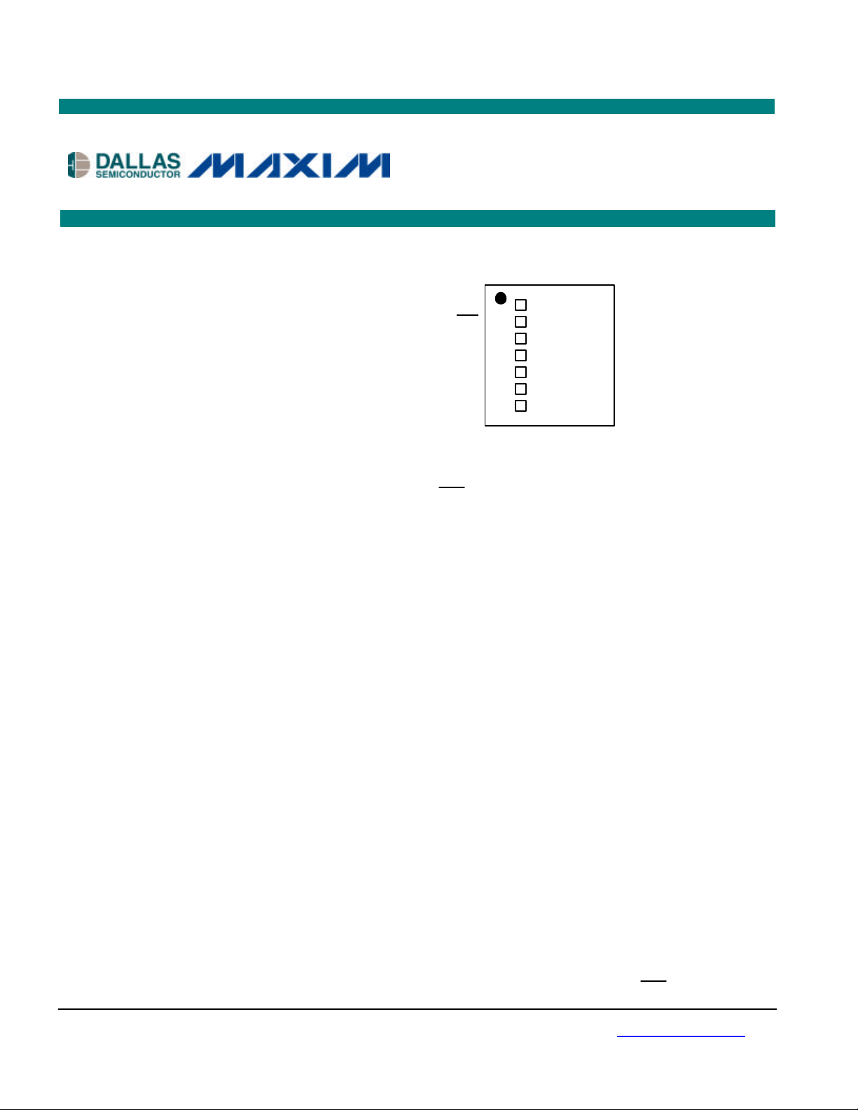
PIN ASSIGNMENT
V
RST
DQ
3
PIN DESCRIPTION
RST - Reset
CLK - Clock
DQ - Data Input/Output
GND - Ground
VCC - +5V
OSC - 1Hz Oscillator Output
NC - No Connect
§ Operating temperature range of 0°C to +70°C
§ Low-profile SIP module
§ Underwriters La boratory (UL) recognized
DESCRIPTION
The DS1603 is a real-time clock/elapsed time counter designed to count seconds when VCC power is
applied and continually count seconds under battery backup power with an additional counter regardless
of the condition of VCC. The continuous counter can be used to derive time of day, week, month, and year
by using a software algorithm. The VCC powered counter will automatically record the amount of time
that VCC power is applied. This function is particularly useful in determining the operational time of
equipment in which the DS1603 is used. Alternatively, this counter can also be used under software
control to record real-time events. Communication to and from the DS1603 takes place via a 3-wire serial
port. A 1-byte protocol selects read/ write functions, counter clear functions and oscillator trim. The
device contains a 32.768kHz crystal that will keep track of time to within ±2 min/mo. An internal lithium
energy source contains enough energy to power the continuous seconds counter for over 10 years.
OPERATION
The main elements of the DS1603 are shown in Figure 1. As shown, communications to and from the
elapsed time counter occur over a 3-wire serial port. The port is activated by driving RST to a high state.
may be simultaneously available through various sales channels. For information about device errata, click here: www.maxim -ic.com/errata.
1 of 8 093002
Page 2

DS1603
With RST at high level 8 bits are loaded into the protocol shift register providing read/write, register
select, register clear, and oscillator trim information. Each bit is serially input on the rising edge of the
clock input. After the first eight clock cycles have loaded the protocol register with a valid protocol
additional clocks will output data for a read or input data for a write. VCC must be present to access the
DS1603. If VCC < VTP, the DS1603 will switch to internal power and disable the serial port to conserve
energy. When running off of the internal power supply, only the continuous counter will continue to
count and the counter powered by VCC will stop, but retain the count, which had accumulated when VCC
power was lost. The 32-bit VCC counter is gated by VCC and the internal 1Hz signal.
PROTOCOL REGISTER
The protocol bit definition is shown in Figure 2. Valid protocols and the resulting actions are shown in
Table 1. Each data transfer to the protocol register designates what action is to occur. As defined, the
MSB (bit 7 which is designated ACC) selects the 32-bit continuous counter for access. If ACC is a logical
1 the continuous counter is selected and the 32 clock cycles that follow the protocol will either read or
write this counter. If the counter is being read, the contents will be latched into a different register at the
end of protocol and the latched contents will be read out on the next 32 clock cycles. This avoids reading
garbled data if the counter is clocked by the oscillator during a read. Similarly, if the counter is to be
written, the data is buffered in a register and all 32 bits are jammed into the counter simultaneously on the
rising edge of the 32nd clock. The next bit (bit 6 which is designated AVC) selects the 32–bit VCC active
counter for access. If AVC is a logical 1 this counter is selected and the 32 clock cycles that follow will
either read or write this counter. If both bit 7 and bit 6 are written to a logic high, all clock cycles beyond
the protocol are ignored and bit 5, 4, and 3 are loaded into the oscillator trim register. A value of binary 3
(011) will give a clock accuracy of ±120 seconds per month at +25°C. Increasing the binary number
towards 7 will cause the real-time clock to run faster. Conversely, lowering the binary number towards 0
will cause the clock to run slower. Binary 000 will stop the oscillator completely. This feature can be used
to conserve battery life during storage. In this mode the internal power supply current is reduced to 100
nA maximum. In applications where oscillator trimming is not practical or not needed, a default setting of
011 is recommended. Bit 2 of protoco l (designated CCC) is used to clear the continuous counter. When
set to logic 1, the continuous counter will reset to 0 when RST is taken low. Bit 1 of protocol (designated
CVC) is used to clear the VCC active counter. When set to logic al 1, the VCC active counter will reset to 0
when RST is taken low. Both counters can be reset simultaneously by setting CCC and CVC both to a
logical 1. Bit 0 of the protocol (designated RD) determines whether the 32 clocks to follow will write a
counter or read a counter. When RD is set to a logical 0 a write action will follow when RD is set to a
logical 1 a read action will follow. When sending the protocol, 8 bits should always be sent. Sending less
than 8 bits can produce erroneous results. If clearing the counters or trimming the oscillator, the data
transfer can be terminated after the 8-bit protocol is sent. However, when reading or writing the counters,
32 clock cycles should always follow the protocol.
RESET AND CLOCK CONTROL
All data transfers are initiated by driving the RST input high. The RST input has two functions. First,
RST turns on the serial port logic, which allows access to the protocol register for the protocol data entry.
Second, the RST signal provides a method of terminating the protocol transfer or the 32-bit counter
transfer. A clock cycle is a sequence of a rising edge followed by a falling edge. For write inputs, data
must be valid during the rising edge of the clock. Data bits are output on the falling edge of the clock
when data is being read. All data transfers terminate if the RST input is transitioned low and the DQ pin
goes to a high-impedance state. RST should only be transitioned low while the clock is high to avoid
disturbing the last bit of data. All data transfers must consist of 8 bits when transferring protocol only or
8 + 32 bits when reading or writing either counter. Data transfer is illustrated in Figure 3.
2 of 9
Page 3

DS1603
DATA INPUT
Following the 8-bit protocol that inputs write mode, 32 bits of data are written to the selected counter on
the rising edge of the next 32 CLK cycles. After 32 bits have been entered any additional CLK cycles will
be ignored until RST is transitioned low to end data transfer and then high again to begin new data
transfer.
DATA OUTPUT
Following the eight CLK cycles that input read mode protocol, 32 bits of data will be output from the
selected counter on the next 32 CLK cycles. The first data bit to be transmitted from the selected 32-bit
counter occurs on the falling edge after the last bit of protocol is written. When transmitting data from the
selected 32-bit counter, RST must remain at high level as a transition to low level will terminate data
transfer. Data is driven out the DQ pin as long as CLK is low. When CLK is high the DQ pin is tristated.
OSCILLATOR OUTPUT
Pin 6 of the DS1603 module is a 1Hz output signal. This signal is present only when VCC is applied and
greater than the internal power supply. However, the output is guaranteed to meet TTL requirement only
while V
is within normal limits. This output can be used as a 1-second interrupt or time tick needed in
CC
some applications.
INTERNAL POWER
The internal battery of the DS1603 module provides 35mAh and will run the elapsed time counter for
over 10 years in the absence of power.
PIN DESCRIPTIONS
VCC, GND – DC power is provided to the device on these pins. V
within normal limits, the device is fully accessible and data can be written and read. When a 3V battery is
connected to the device and V
V
the continuous counter is switched over to the internal battery.
BAT
is below 1.25 x V
CC
, reads and writes are inhibited. As V
BAT
CLK (Serial Clock Input) – CLK is used to synchronize data movement on the serial interface.
DQ (Data Input/Output) – The DQ pin is the bi-directional data pin for the 3-wire interface.
RST (Reset) – The reset signal must be asserted high during a read or a write.
OSC (One Hertz Output Signal) – This signal is only present when Vcc is at a valid level and the
oscillator is enabled.
is the +5V input. When 5V is applied
CC
falls below
CC
3 of 9
Page 4

Figure 1. ELAPSED TIME COUNTER BLOCK DIAGRAM
DS1603
Figure 2. PROTOCOL BIT MAP
7 6 5 4 3 2 1 0
ACC AVC OSC2 OSC1 OSC0 CCC CVC RD
4 of 9
Page 5

Table 1. VALID PROTOCOLS
ACTION
ACC AVC OSC2 OSC1 OSC0 CCC CVC RD
Read
Continuous
1 0 X X X X X 1
Counter
Write
Continuous
1 0 X X X X X 0
Counter
Read VCC
Active
0 1 X X X X X 1
Counter
Write VCC
Active
0 1 X X X X X 0
Counter
Clear
Continuous
0 0 X X X 1 X X
Counter
Clear VCC
Active
0 0 X X X X 1 X
Counter
Set Oscillator
Trim Bits
1 1 A B C X X 0
X = Don’t Care
PROTOCOL
DS1603
FUNCTION
Output continuous
counter on the 32 clocks
following protocol.
Oscillator trim register
is not updated. Counters
are not reset.
Input data to continuous
counter on the 32 clocks
following protocol.
Oscillator trim register
is not updated. Counters
are not reset.
Output VCC active
counter on the 32 clocks
following protocol,
oscillator trim register
is not updated. Counters
are not reset.
Input data to continuous
counter on the 32 clocks
following protocol.
Oscillator trim register
is not updated. Counters
are not reset.
Resets the continuous
counter to all zeros at
the end of protocol.
Oscillator trim register
is not updated.
Resets the VCC active
counter to all zeros at
the end of protocol.
Oscillator trim register
is not updated.
Sets the oscillator trim
register to a value of
ABC. Counters are
unaffected.
5 of 9
Page 6

Figure 3. DATA TRANSFER
DS1603
TIMING DIAGRAM: READ/WRITE DATA TRANSFER
Note: tCL, tCH, tR, and tF apply to both read and write data transfer.
6 of 9
Page 7
DS1603
ABSOLUTE MAXIMUM RATINGS
Voltage Range on Any Pin Relative to Ground -0.3V to +7.0V
Operating Temperature Range 0°C to +70°C
Storage Temperature Range -40°C to +70°C
Soldering Temperature Range See IPC/JEDEC J-STD-020A (See Note 11)
This is a stress rating only and functional operation of the device at these or any other conditions beyond those indicated in the operation
sections of this specification is not implied. Exposure to absolute maximum rating conditions for extended periods of time can affect reliability.
RECOMMENDED DC OPERATING CONDITIONS (0°C to +70°C)
PARAMETER SYMBOL MIN TYP MAX UNITS NOTES
Supply Voltage VCC 4.5 5.0 5.5 V 1
Logic 1 Input VIH 2.0 VCC + 0.3 V 1
Logic 0 Input VIL -0.3 0.8 V 1
DC ELECTRICAL CHARACTERISTICS (0°C to +70°C; VCC = 5V ±10%)
PARAMETER SYMBOL MIN TYP MAX UNITS NOTES
Input Leakage ILI -1 +1 µA
I/O Leakage ILO -1 +1 µA
Logic 1 Output VOH 2.4 V 2
Logic 0 Output VOL 0.4 V 3
Active Supply Current ICC 1 mA 4
Timekeeping Current I
50 µA 5
CC1
Battery Trip Point VTP 3.0 4.5 V 9
CAPACITANCE (TA = +25°C)
PARAMETER SYMBOL MIN TYP MAX UNITS NOTES
Input Capacitance CI 5 pF
I/O Capacitance C
10 pF
I/O
7 of 9
Page 8

DS1603
AC ELECTRICAL CHARACTERISTICS (VCC = +5V ±10%; 0°C to +70°C)
PARAMETER SYMBOL MIN TYP MAX UNITS NOTES
Data to CLK Setup tDC 50 ns 6
CLK to Data Hold t
CLK to Data Delay t
60 ns 6
CDH
200 ns 6, 7, 8
CDD
CLK Low Time tCL 250 ns 6
CLK High Time tCH 250 ns 6
CLK Frequency f
CLK Rise and Fall t
RST to CLK Setup
CLK to RST Hold t
RST Inactive Time
RST Low to I/O High-Z
CLK High to I/O High-Z t
DC 2.0 MHz 6
CLK
500 ns
F, tR
tCC 100 ns 6
60 ns 6
CCH
t
1 µs 6
CWH
t
70 ns 6
RDZ
20 ns 6
CDZ
(TA = +25°C)
PARAMETER SYMBOL MIN TYP MAX UNITS NOTES
Expected Data
Retention Time
tDR 10 years 10
NOTES:
1) All voltages are referenced to ground.
2) Logic 1 voltages are specified at a source current of 1mA.
3) Logic 0 voltages are specified at a sink current of 4mA.
4) I
5) I
6) Measured at V
7) Measured at VOH = 2.4V or VOL - 0.4V.
8) Load capacitance = 50pF.
9) Battery trip point is the point at which the VCC powered counter and the serial port stops operation.
10) The expected t
11) Real-time clock modules can be successfully processed through conventional wave-soldering
is specified with the DQ pin open.
CC
is specified with V
CC1
IH
= 2.0V or V
at 5.0V and RST = GND.
CC
= 0.8V.
IL
The battery trip point drops below the minimum once the internal lithium energy cell is exhausted.
is defined as accumulative time in the absence of V
DR
with the clock oscillator
CC
running.
techniques as long as temperature exposure to the lithium energy source contained within does not
exceed +85°C. Post-solder cleaning with water-washing techniques is acceptable, provided that
ultrasonic vibration is not used.
8 of 9
Page 9

DS1603 7-PIN MODULE
PKG 7-PIN
DIM MIN MAX
A IN.
MM
B IN.
MM
C IN.
MM
D IN.
MM
E IN.
MM
F IN.
MM
G IN.
MM
H IN.
MM
J IN.
MM
0.830
21.08
0.650
16.51
0.310
7.87
0.015
0.38
0.110
2.79
0.015
0.38
0.090
2.29
0.105
2.67
0.360
9.14
0.850
21.59
0.670
17.02
0.330
8.38
0.030
0.76
0.140
3.56
0.021
0.53
0.110
2.79
0.135
3.43
0.390
9.91
DS1603
9 of 9
 Loading...