

Page 1
Note:
Some revisions of this device may inco
rporate deviations from published specifications known as errata. Multiple revisions of any device
DS1558
Watchdog Clock with
NV RAM Control
www.
maxim
-ic.com
www.maxim
-
ic.com
A18
A16
A12A6A4A3A2A1A5A7A14
N.C.
VCCO
1 2 3 4 5 6 7 8 10 12 35 36
VCC N.C.
A16 GND RST NC N.C. DQ0
DQ1DQ2
DQ6
VBAT1
WE
IRQ/FT
A8 OE
A10 CE
X1 GND VBAT
2
A15 A13 OER A9 A11 34 33 32 31 30 29 28 27 26 25
24 23 22 21 20 19 18 17 16 15 14 13
11 9
484746454443424140393837CER
DQ7
DQ5
DQ4
DQ3
GND
A0
X2 N.C.
FEATURES
§ Integrated real-time clock (RTC), power-fail
control circuit, and NV RAM controller
§ Clock registers are accessed identically to the
static RAM; these registers are resident in the
16 top RAM locations
§ Century register
§ Greater than 10 ye ars of timekeeping and data
retention in the absence of power with small
lithium coin cell(s) and low-leakage SRAM
§ Precision power-on reset
§ Programmable watchdog timer and RTC
alarm
§ BCD-coded year, month, date, day, hours,
minutes, and seconds with automatic leapyear compensation valid up to the year 2100
§ Battery voltage -level indicator flag
§ Power-fail write protection allows for ±10%
VCC power-supply tolerance
§ Underwriters Laboratory (UL) recognized
ORDERING INFORMATION
PART
PIN-
PACKAGE
V
CC
(V)
DS1558Y 48 TQFP 5 DS1558B
DS1558W 48 TQFP 3.3 DS1558D
TOP
MARK
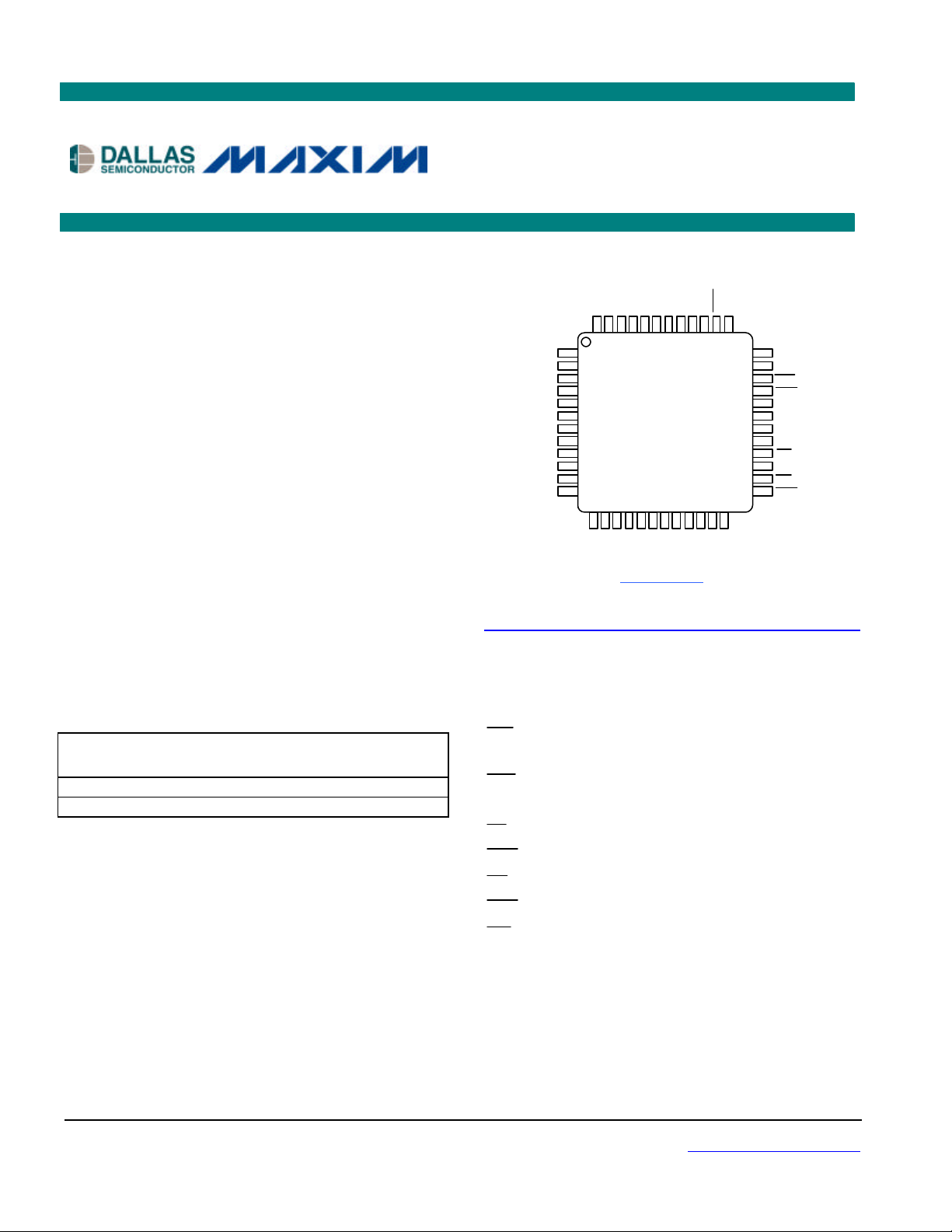
PIN ASSIGNMENT (Top View)
DS1558
48-Pin TQFP
Package Dimension Information
http://www.maxim-ic.com/TechSupport/DallasPackInfo.htm
PIN DESCRIPTION
A0–A18 - Address Input
DQ0–DQ7 - Data Input/Outputs
IRQ\FT - Interrupt, Frequency-Test
Output (Open Drain)
RST - Power-On Reset Output
(Open Drain)
CE - Chip-Enable Input
CER - Chip-Enable RAM
OE - Output-Enable Input
OER - Output-Enable RAM
WE - Write Enable
V
- Power-Supply Input
CC
V
- VCC Out to RAM
CCO
GND - Ground
N.C. - No Connection
X1, X2 - Crystal Connection
V
BAT1
V
BAT2
may be simultaneously available through various sales channels. For information about device errata, click here: http://www.maxim -ic.com/errata.
1 of 18 072402
- +3V Battery Input
- +3V Battery Input
Page 2
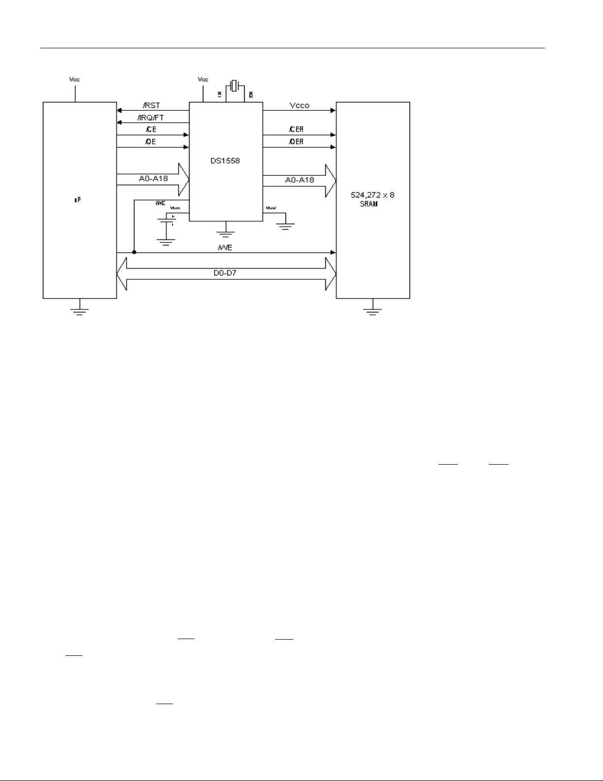
TYPICAL OPERATING CIRCUIT
DS1558
DESCRIPTION
The DS1558 is a full function, year 2000-compliant (Y2KC), real-time clock/calendar with an RTC
alarm, watchdog timer, power-on reset, battery monitor, and NV SRAM controller. User access to all
registers within the DS1558 is accomplished with a byte-wide interface as shown in Figure 1. The RTC
registers contain century, year, month, date, day, hours, minutes, and seconds data in 24-hour BCD
format. Corrections for day of month and leap year are made automatically.
The DS1558 maps the RTC registers into the SRAM address space and constantly monitors A0–A18.
When any of the upper 16 address locations are accessed, the DS1558 inhibits CER and OER to the
SRAM, and redirects reads and writes to the RTC registers within the DS1558. The DS1558 can be used
with SRAMs up to 524,272 addresses. Smaller SRAMs can be used, provided that the unused upper
address lines on the DS1558 are connected to VCC.
The RTC registers are double-buffered into an internal and external set. The user has direct access to the
external set. Clock/calendar updates to the external set of registers can be disabled and enabled to allow
the user to access static data. Assuming the internal oscillator is turned on, the internal set of registers is
continuously updated; this occurs regardless of external register settings to guarantee that accurate RTC
information is always maintained.
The DS1558 has interrupt (
The
IRQ /FT interrupt output can be used to generate an external interrupt when the RTC register values
IRQ /FT) and reset ( RST ) outputs that can be used to control CPU activity.
match user-programmed alarm values. The interrupt is always available while the device is powered from
the system supply, and it can be programmed to occur when in the battery-backed state to serve as a
system wake-up. The
IRQ /FT output can also be used as a CPU watchdog timer. CPU activity is
monitored and an interrupt or reset output are activated if the correct activity is not detected within
2 of 18
Page 3
DS1558
programmed limits. The DS1558 power-on reset can be used to detect a system power-down or failure
and hold the CPU in a safe reset state until normal power returns and stabilizes; the RST output is used
for this function.
The DS1558 also contains its own power-fail circuitry, which automatically protects the data in the clock
and SRAM against out-of-tolerance V
enters an out-of-tolerance condition. When V
conditions by inhibiting the CE input when the VCC supply
CCI
goes below the level of V
CCI
, the external battery is
BAT
switched on to supply energy to the clock and the external SRAM. This feature provides a high degree of
data security during unpredictable system operation brought on by low VCC levels.
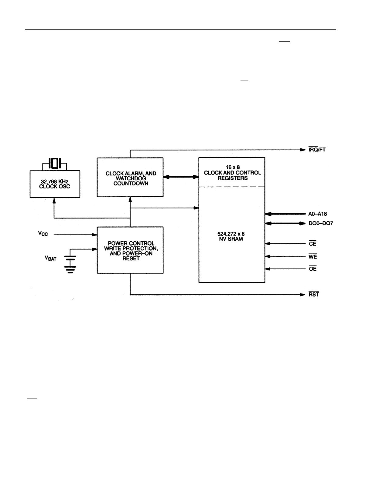
Figure 1. BLOCK DIAGRAM
Note: Any unused upper address pins must be connected to VCC to properly address the RTC.
SIGNAL DESCRIPTIONS
A0–A18 – Address inputs for address decode. The DS1558 uses the address inputs to determine whether
or not a read or write cycle should be directed to the attached SRAM or to the RTC registers.
DQ0–DQ7 – Data input/output pins for the RTC registers.
IRQ /FT – This pin is used to output the alarm interrupt or the frequency test signal. It is open drain and
requires an external pullup resistor.
3 of 18
Page 4

DS1558
RST – This pin is an output used to signal that V
is out of tolerance. On power-up, RST is held low for
CC
a period of time to allow the system to stabilize. The RTC and SRAM are not accessible while RST is
active. This pin is open drain and requires an external pullup resistor.
CE – Chip-enable input that is used to access the RTC and the external SRAM.
CER – Chip-enable RAM output. CE is passed through to CER , with an added propagation delay. When
the signals on A0–A18 match an RTC address,
CER is held high, disabling the SRAM. If OE is also low,
the RTC outputs data on DQ0–DQ7.
OE – Output-enable input that is used to access the RTC and the external SRAM.
OER – Output-enable RAM output. OE is passed through to OER , with an added propagation delay.
When the signals on A0–A18 match an RTC address, CER is held high, disabling the SRAM. If CE is
also low, the RTC outputs data on DQ0–DQ7.
WE – Write-enable input that is used to write data to the RTC registers.
VCC, GND – DC power is provided to the device on these pins. VCC is the +5V input. When 5V (or 3.3V
for the 3.3V version) is applied within normal limits, the device is fully accessible and data can be written
and read. Reads and writes are inhibited when a 3V battery is connected to the device and VCC is VTP.
However, the timekeeping function continues unaffected by the lower input voltage. As VCC falls below
V
, the RAM and RTC are switched over to the external power supply (nominal 3.0V DC) at V
BAT
BAT
.
V
– VCC output to RAM. While VCC is above V
CCO
VCC is below the battery level, the SRAM is powered by one of the V
, the external SRAM is powered by VCC. When
BAT
inputs.
BAT
N.C. – No internal connection.
X1, X2 – Connections for a standard 32.768kHz quartz crystal. The internal oscillator circuitry is
designed for operation with a crystal having a specified load capacitance (C
) of 6pF. For more
L
information about crystal selection and crystal layout considerations, refer to Application Note 58
“Crystal Considerations with Dallas Real-Time Clocks.” The DS1558 can also be driven by an external
32.768kHz oscillator. In this configuration, the X1 pin is connected to the external oscillator signal and
the X2 pin is floated.
V
BAT1
, V
– Battery inputs for any standard 3V lithium cell or other energy source. Battery voltage
BAT2
must be held between 2.5V and 3.7V for proper operation. UL recognized to ensure against reverse
charging current when used with a lithium battery. If only one battery is used, it should be attached to
V
BAT1
, and V
should be grounded.
BAT2
See “Conditions of Acceptability” at http://www.maxim-ic.com/TechSupport/QA/ntrl.htm.
4 of 18
Page 5
Table 1. OPERATING MODES
DS1558
V
CC
VCC > V
PF
VSO < VCC < V
VCC < VSO < V
CE OE WE
V
IH
V
IL
V
IL
V
IL
X X X High-Z Deselect CMOS Standby
PF
X X X High-Z Data Retention Battery Current
PF
X X High-Z Deselect Standby
XVILD
V
V
IL
IH
V
V
DQ0–DQ7 MODE POWER
Write Active
Read Active
IH
IH
IN
D
OUT
High-Z Read Active
DATA READ MODE
The DS1558 is in the read mode whenever CE is low and WE is high. The device architecture allows
ripple-through access to any valid address location. Valid data is available at the DQ pins within t
the last address input is stable, provided that
times are not met, valid data is available at the latter of chip-enable access (t
access time (t
). The state of the data input/output pins (DQ) is controlled by CE and OE . If the
OEA
CE and OE access times are satisfied. If CE or OE access
) or at output-enable
CEA
AA
after
outputs are activated before tAA, the data lines are driven to an intermediate state until tAA. If the address
inputs are changed while CE and OE remain valid, output data remains valid for output-data hold time
(tOH), but then goes indeterminate until the next address access.
DATA WRITE MODE
The DS1558 is in the write mode whenever WE and CE are in their active state. The start of a write is
referenced to the latter occurring transition of WE or CE . The addresses must be held valid throughout
the cycle. CE and WE must return inactive for a minimum of tWR prior to the initiation of a subsequent
read or write cycle. Data in must be valid tDS prior to the end of the write and remain valid for t
afterward. In a typical application, the OE signal is high during a write cycle. However, OE can be active
provided that care is taken with the data bus to avoid bus contention. If OE is low prior to WE
transitioning low, the data bus can become active with read data defined by the address inputs. A low
transition on WE then disables the outputs t
after WE goes active.
WEZ
DH
DATA RETENTION MODE
The 5V device is fully accessible and data can be written and read only when VCC is greater than VPF.
However, when VCC is below the power-fail point VPF (point at which write protection occurs), the
internal clock registers and SRAM are blocked from any access. When VCC falls below the battery switch
point V
operation and SRAM data are maintained from the battery until VCC is returned to nominal levels.
The 3.3V device is fully accessible and data can be written and read only when V
When VCC falls below VPF, access to the device is inhibited. If VPF is less than VSO, the device power is
switched from V
than VSO, the device power is switched from VCC to the internal backup lithium battery when VCC drops
below V
nominal levels.
All control, data, and address signals must be powered down when V
(battery supply level), device power is switched from the VCC pin to the backup battery. RTC
SO
is greater than VPF.
CC
to the internal backup lithium battery when VCC drops below VPF. If VPF is greater
CC
. RTC operation and SRAM data are maintained from the battery until VCC is returned to
SO
is powered down.
CC
5 of 18
Page 6

DS1558
BATTERY LONGIVITY
The battery lifetime is dependent on the RAM battery standby current and the DS1558 internal clock
oscillator current. The total battery current is I
OSC
+ I
. When VCC is above VPF, I
CCO
current is less than
BAT
50nA. The DS1558 has an internal circuit to prevent battery charging. No external protection components
are required, and none should be used. The DS1558 has two battery pins that operate independently; the
DS1558 selects the higher of the two inputs. If only one battery is used, the battery should be attached to
V
BAT1
, and V
should be grounded.
BAT2
INTERNAL BATTERY MONITOR
The DS1558 constantly monitors the battery voltage of the internal battery. The battery-low flag (BLF)
bit of the flags register (B4 of 7FFF0h) is not writable and should always be a 0 when read. If a 1 is ever
present, both battery inputs are below 1.8V and both the contents of the RTC and RAM are questionable.
POWER-ON RESET
A temperature-compensated comparator circuit monitors the level of VCC. When VCC falls to the powerfail trip point, the
signal continues to be pulled low for a period of 40ms to 200ms. The power-on reset function is
independent of the RTC oscillator and thus is operational whether or not the oscillator is enabled.
RST signal (open drain) is pulled low. When V
returns to nominal levels, the RST
CC
6 of 18
Page 7

DS1558
CLOCK OPERATIONS
Table 2 and the following paragraphs describe the operation of the RTC, alarm, and watchdog functions.
Table 2. DS1558 REGISTER MAP
ADDRESS
B
7
B
6
B
5
DATA
B
4
B
3
B
B
2
B
1
0
FUNCTION/RANGE
7FFFFh 10 YEAR YEAR YEAR 00–99
7FFFEh X X X 10 M MONTH MONTH 01–12
7FFFDh X X 10 DATE DATE DATE 01–31
7FFFCh X FT X X X DAY DAY 01–07
7FFFBh X X 10 HOUR HOUR HOUR 00–23
7FFFAh X 10 MINUTES MINUTES MINUTES 00–59
7FFF9h
OSC
10 SECONDS SECONDS SECONDS 00–59
7FFF8h W R 10 CENTURY CENTURY CONTROL 00–39
7FFF7h WDS BMB4 BMB3 BMB2 BMB1 BMB0 RB1 RB0 WATCHDOG —
7FFF6h AE Y ABE Y Y Y Y Y INTERRUPTS —
7FFF5h AM4 Y 10 DATE DATE ALARM DATE 01–31
7FFF4h AM3 Y 10 HOURS HOURS ALARM HOURS 00–23
7FFF3h AM2 10 MINUTES MINUTES ALARM MINUTES 00–59
7FFF2h AM1 10 SECONDS SECONDS ALARM SECONDS 00–59
7FFF1h Y Y Y Y Y Y Y Y UNUSED —
7FFF0h WF AF 0 BLF 0 0 0 0 FLAGS —
X = Unused, Read/Writeable Under Write and Read Bit Control AE = Alarm Flag Enable
FT = Frequency Test Bit Y = Unused, Read/Writeable Without Write and Read Bit Control
OSC = Oscillator Start/Stop Bit
W = Write Bit AM1–AM4 = Alarm Mask Bits
R = Read Bit WF = Watchdog Flag
WEN = Watchdog Enable Bit AF = Alarm Flag
BMB0–BMB4 = Watchdog Multiplier Bits 0 = Reads as a 0 and Cannot Be Changed
RB0–RB1 = Watchdog Resolution Bits BLF = Battery Low Flag
ABE = Alarm in Backup-Battery Mode Enable
CLOCK OSCILLATOR CONTROL
The oscillator can be turned off to minimize current drain from the battery. The OSC bit is the MSB of
the seconds register (B7 of 7FFF9h). Setting OSC to a 1 stops the oscillator; setting to a 0 starts the
oscillator. The initial state of OSC is not guaranteed. When power is applied for the first time, the OSC
bit should be enabled. Oscillator operation and frequency can be verified by setting the FT bit and
monitoring the
IRQ /FT pin for 512Hz.
OSCILLATOR STARTUP TIME
Oscillator startup times are highly dependent upon crystal characteristics and layout. High ESR and
excessive capacitive loads are the major contributors to long startup times. A circuit using a crystal with
the recommended characteristics and following the recommended layout usually starts within 1 second.
7 of 18
Page 8

DS1558
READING THE CLOCK
When reading the RTC data, it is recommended to halt updates to the external set of double-buffered
RTC registers. This puts the external registers into a static state, allowing data to be read without register
values changing during the read process. Normal updates to the internal registers continue while in this
state. External updates are halted when a 1 is written into the read bit, B6 of the control register
(7FFF8h). As long as a 1 remains in the control register read bit, updating is halted. After a halt is issued,
the registers reflect the RTC count (day, date, and time) that was current at the moment the halt command
is issued. Normal updates to the external set of registers resume within 1 second after the read bit is set to
a 0 for a minimum of 500ms. The read bit must be a 0 for a minimum of 500ms to ensure the external
registers are updated.
SETTING THE CLOCK
The MSB bit, B7, of the control register is the write bit. Setting the write bit to a 1, like the read bit, halts
updates to the 7FFF8h–7FFFFh registers. After setting the write bit to a 1, RTC registers can be loaded
with the desired RTC count (day, date, and time) in 24-hour BCD format. Setting the write bit to a 0 then
transfers the values written to the internal RTC registers and allows normal operation to resume.
CLOCK ACCURACY
The accuracy of the clock is dependent upon the accuracy of the crystal and the accuracy of the match
between the capacitive load of the oscillator circuit and the capacitive load for which the crystal was
trimmed. Additional error is added by the crystal-frequency drift caused by temperature shifts. External
circuit noise coupled into the oscillator circuit can result in the clock running fast. Refer to Application
Note 58 “Crystal Considerations with Dallas Real-Time Clocks” for detailed information.
FREQUENCY TEST MODE
The DS1558 frequency test mode uses the open-drain IRQ /FT output. With the oscillator running, the
IRQ /FT output toggles at 512Hz when the FT bit is a 1, the alarm-flag enable bit (AE) is a 0, and the
watchdog-enable bit (WDS) is a 1, or the watchdog register is reset (register 7FFF7h = 00h). The IRQ /FT
output and the frequency test mode can be used as a measure of the actual frequency of the 32.768kHz
RTC oscillator. The IRQ /FT pin is an open-drain output that requires a pullup resistor for proper
operation. The FT bit is cleared to a 0 on power-up.
USING THE CLOCK ALARM
The alarm settings and control for the DS1558 reside within registers 7FFF2h–7FFF5h. Register 7FFF6h
contains two alarm-enable bits: alarm enable (AE) and alarm in backup enable (ABE). The AE and ABE
bits must be set as described below for the
The alarm can be programmed to activate on a specific day of the month or repeat every day, hour,
minute, or second. It can also be programmed to go off while the DS1558 is in the battery-backed state of
operation to serve as a system wake-up. Alarm mask bits AM1–AM4 control the alarm mode. Table 3
shows the possible settings. Configurations not listed in the table default to the once-per-second mode to
notify the user of an incorrect alarm setting.
IRQ /FT output to be activated for a matched alarm condition.
8 of 18
Page 9

DS1558
Table 3. ALARM MASK BITS
AM4 AM3 AM2 AM1 ALARM RATE
1111Once per second
1110When seconds match
1100When minutes and seconds match
1000When hours, minutes, and seconds match
0000When date, hours, minutes, and seconds match
When the RTC register values match alarm register settings, AF is set to a 1. If AE is also set to a 1, the
alarm condition activates the IRQ /FT pin. The IRQ /FT signal is cleared by a read or write to the flags
register (address 7FFF0h). When CE is active, the IRQ /FT signal can be cleared by having the address
stable for as short as 15ns and either
OE or WE active, but is not guaranteed to be cleared unless t
fulfilled (Figure 2). Once the address has been selected for at least 15ns, the
IRQ /FT signal can be cleared
RC
is
immediately, but is not guaranteed to be cleared until tRC is fulfilled (Figure 3). The alarm flag is also
cleared by a read or write to the flags register, but the flag does not change states until the end of the
read/write cycle and the IRQ /FT signal has been cleared.
The IRQ /FT pin can also be activated in the battery-backed mode. The IRQ /FT goes low if an alarm
occurs and both ABE and AE are set. The ABE and AE bits are cleared during the power-up transition,
but an alarm generated during power-up sets AF. Therefore, the AF bit can be read after system power-up
to determine if an alarm was generated during the power-up sequence. Figure 4 illustrates alarm timing
during the backup-battery mode and power-up states.
Figure 2. CLEARING IRQ WAVEFORMS ACTIVE
Figure 3. CLEARING IRQ WAVEFORMS
9 of 18
Page 10

DS1558
Figure 4. BACKUP MODE ALARM WAVEFORMS
USING THE WATCHDOG TIMER
The watchdog timer can be used to detect an out-of-control processor. The user programs the watchdog
timer by setting the desired amount of timeout into the 8-bit watchdog register (address 7FFF7h). The
five watchdog register bits BMB4–BMB0 store a binary multiplier and the two lower-order bits
RB1–RB0 select the resolution, where 00 = 1/16 second, 01 = 1/4 second, 10 = 1 second, and
11 = 4 seconds. The watchdog timeout value is then determined by the multiplication of the 5-bit
multiplier value with the 2-bit resolution value. (For example: writing 00001110 in the watchdog register
= 3 x 1 second or 3 seconds.) If the processor does not reset the timer within the specified period, the
watchdog flag (WF) is set and a processor interrupt is generated and stays active until either WF is read
or the watchdog register (7FFF7h) is read or written.
The MSB of the watchdog register is the watchdog steering bit (WDS). When set to a 0, the watchdog
activates the IRQ /FT output when the watchdog times out. WDS should not be written to a 1, and should
be initialized to a 0 if the watchdog function is enabled.
The watchdog timer resets when the processor performs a read or write of the watchdog register. The
timeout period then starts over. The watchdog timer is disabled by writing a value of 00h to the watchdog
register. The watchdog function is automatically disabled upon power-up and the watchdog register is
cleared.
POWER-ON DEFAULT STATES
Upon application of power to the device, the following register bits are set to a 0:
WDS = 0, BMB0–BMB4 = 0, RB0–RB1 = 0, AE = 0, and ABE = 0
All other bits are undefined.
10 of 18
Page 11

DS1558
ABSOLUTE MAXIMUM RATINGS*
Voltage Range on Any Pin Relative to Ground -0.3V to +6.0V
Storage Temperature Range -55°C to +125°C
Soldering Temperature Range See IPC/JEDEC J-STD-020A
*This is a stress rating only and functional operation of the device at these or any other conditions beyond those indicated in the operation
sections of this specification is not implied. Exposure to absolute maximum rating conditions for extended periods of time can affect reliability.
RECOMMENDED DC OPERATING CONDITIONS
(VCC = 3.3V ±10% or 5V ±10%, TA = -40°C to +85°C)
PARAMETER SYMBOL MIN TYP MAX UNITS NOTES
Logic 1 Voltage (All Inputs)
VCC = +5V ±10%
VCC = +3.3V ±10%
Logic 0 Voltage (All Inputs)
VCC = +5V ±10% V
VCC = +3.3V ±10%
Battery Voltage V
V
V
V
IH
IH
IL
IL
BAT
2.2 VCC + 0.3V V 1
2.0 VCC + 0.3V V 1
-0.3 +0.8 1
-0.3 +0.6 1
2.5 3.3 3.7 V
11 of 18
Page 12

DC ELECTRICAL CHARACTERISTICS
PARAMETER SYMBOL MIN TYP MAX UNITS NOTES
(V
= +3.3V ±10% or +5V ±10%, TA = -40°C to +85°C)
CC
DS1558
Active Supply Current, +5V I
Active Supply Current, +3.3V I
TTL Standby, +5V ( CE = VIH)
TTL Standby, +3.3V ( CE = VIH)
I
I
CMOS Standby Current, +5V
(
CE ³ V
- 0.2V)
CC
I
CMOS Standby Current, +3.3V
(
CE ³ V
- 0.2V)
CC
I
Input Leakage Current
(Any Input)
Output Leakage Current
(Any Output)
Output Logic 1 Voltage
= -1.0mA)
(I
OUT
V
Output Logic 0 Voltage
I
= 2.1mA, DQ0–DQ7
OUT
V
Outputs
I
= 7.0mA, IRQ /FT and
OUT
RST Outputs
V
Write Protection Voltage, +5V V
CC1
CC1
CC2
CC2
I
I
CC
CC
IL
OL
OH
OL1
OL2
PF
6 25 mA 2, 3
4 15 mA 2, 3
3 6 mA 2, 3
2 6 mA 2, 3
2 6 mA 2, 3
1 2 mA 2, 3
-1 +1
-1 +1
mA
mA
2.4 V 1
0.4 V 1
0.4 V 1, 5
4.25 4.37 4.50 V 1
Write Protection Voltage, +3.3V V
Battery Switchover Voltage, +5V V
Battery Switchover Voltage, +3.3V V
Battery Current OSC On I
Battery Current OSC Off I
Output Voltage I
Output Voltage I
Output Voltage I
= 70mA, +5V V
CCO
= 40mA, +3.3V V
CCO
= 10µA V
CCO
CRYSTAL SPECIFICATIONS
PF
SO
SO
OSC
BACKUP
CC01
CC01
CC02
*
2.80 2.88 2.97 V 1
V
BAT
V
PF
V1
V 1, 4
0.3 0.5 µA 6,7
100 nA 7
V
- 0.3 V
CC1
V
- 0.3 V
CC1
V
- 0.2 V
BAT
- 0.031 V 10
BAT
PARAMETER SYMBOL MIN TYP MAX UNITS NOTES
Nominal Frequency F
O
Series Resistance ESR 45 kΩ
Load Capacitance C
*The crystal, traces, and crystal input pins should be isolated from RF generating signals. Refer to Application Note 58 “Crystal Considerations
for Dallas Real-Time Clocks” for additional specifications.
L
32.768 kHz
6pF
12 of 18
Page 13

DS1558
READ CYCLE, AC CHARACTERISTICS
(VCC = +3.3V ±10% or +5V ±10%, TA = -40°C to +85°C)
PARAMETER SYMBOL
Read Cycle Time t
Address Access Time t
CE to DQ Low-Z
CE Access Time
CE Data Off Time
OE to DQ Low-Z
OE Access Time
OE Data Off Time
Output Hold from
Address
CE to CER Propagation
t
Delay, +5V
OE to OER Propagation
t
Delay, +5V
CE to CER Propagation
t
Delay, +3.3V
RC
AA
t
CEL
t
CEA
t
CEZ
t
OEL
t
OEA
t
OEZ
t
OH
CEPD
OEPD
CEPD
VCC = +5.5V ±10% VCC = +3.3V ±10%
UNITS NOTES
MIN MAX MIN MAX
70 120 ns
70 120 ns
55ns
70 120 ns
25 40 ns
55ns
35 100 ns
25 35 ns
55ns
15 ns
20 ns
30 ns
OE to OER Propagation
Delay, +3.3V
t
OEPD
Figure 5. READ CYCLE TIMING DIAGRAM
40 ns
13 of 18
Page 14

WRITE CYCLE, AC CHARACTERISTICS
(V
= +3.3V ±10% or +5V ±10%, TA = -40°C to +85°C)
CC
DS1558
PARAMETER SYMBOL
UNITS NOTES
MIN MAX MIN MAX
VCC = +5.0V ±10% VCC = +3.3V ±10%
Write Cycle Time t
Address Access Time t
WE Pulse Width
CE Pulse Width
t
Data Setup Time t
Data Hold Time t
Data Hold Time t
Address Hold Time t
Address Hold Time t
WE Data Off Time
Write Recovery Time t
WC
AS
WEW
t
CEW
DS
DH1
DH2
AH1
AH2
t
WEZ
WR
70 120 ns
00ns
50 100 ns
60 110 ns
30 80 ns
5 5 ns 8
5 5 ns 9
5 0 ns 8
5 5 ns 9
25 40 ns
510ns
Figure 6. WRITE CYCLE TIMING, WRITE-ENABLE CONTROLLED
14 of 18
Page 15

Figure 7. WRITE CYCLE TIMING, CHIP-ENABLE CONTROLLED
DS1558
15 of 18
Page 16

DS1558
POWER-UP/DOWN CHARACTERISTICS (V
= +5V ±10%, TA = -40°C to +85°C)
CC
PARAMETER SYMBOL MIN TYP MAX UNITS NOTES
CE or WE at V
Before Power-Down
VCC Fall Time: V
VCC Fall Time: V
VCC Rise Time: V
VPF to RST High
,
IH
PF(MAX)
PF(MIN)
PF(MIN)
to V
to V
to V
PF(MIN)
SO
PF(MAX)
t
t
t
t
REC
PD
t
FB
0
F
300
10
R
0
40 200 ms
Figure 8. +5V POWER-UP/DOWN WAVEFORM TIMING
ms
ms
ms
ms
16 of 18
Page 17

DS1558
POWER-UP/DOWN CHARACTERISTICS (V
= +3.3V ±10%, TA = -40°C to +85°C)
CC
PARAMETER SYMBOL MIN TYP MAX UNITS NOTES
CE or WE at V
Before Power-Down
VCC Fall Time: V
VCC Rise Time: V
VPF to RST High
,
IH
PF(MAX)
PF(MIN)
to V
to V
PF(MIN)
PF(MAX)
t
t
REC
PD
t
t
0
F
R
300
0
40 200 ms
Figure 9. +3.3V POWER-UP/DOWN WAVEFORM TIMING
ms
ms
ms
CAPACITANCE (T
PARAMETER SYMBOL MIN TYP MAX UNITS NOTES
Capacitance On All Input Pins C
Capacitance On IRQ /FT, RST , and
C
DQ Pins
IN
IO
17 of 18
7pF 1
10 pF 1
= +25°C)
A
Page 18

AC TEST CONDITIONS
Output Load: 25pF
Input Pulse Levels: 0V to +3V
Timing Measurement Reference Levels:
Input: +1.5V
Output: +1.5V
Input Pulse Rise and Fall Times: 5ns
NOTES:
1) Voltage referenced to ground.
2) Typical values are at +25°C and nominal supplies.
3) Outputs are open.
4) Battery switchover occurs at the lower of either the battery voltage or VPF.
5) The IRQ /FT and RST outputs are open drain.
6) Using the recommended crystal on X1 and X2.
DS1558
7) V
8) t
9) t
, CER , and OER pins open.
CCO
, t
AH1
AH2
are measured from WE going high.
DH1
, t
are measured from CE going high.
DH2
10) Typical measured with V
at 3.0V. Typical with I
BAT
= 100µA and V
CCO
= 3.0V is V
BAT
- 0.322.
BAT
18 of 18
 Loading...