

Page 1
www.dalsemi.com
A
A
A
A11A
A
A8A
A
A
A
A
A
A
A
A13A8A9A
A
DS1554
256K NV Y2KC Timekeeping RAM
FEATURES
Integrated NV SRAM, real time clock,
crystal, power-fail control circuit and lithium
energy source
Clock registers are accessed ident ically to the
static RAM; these registers are resident in the
16 top RAM locations
Century byte register; i.e., Y2K complaint
Totally nonvolatile with over 10 years of
operation in the absence of power
Precision power-on reset
Programmable watchdog timer and RTC
alarm
BCD coded year, month, date, day, hours,
minutes, and seconds with automatic leap
year compensation valid up to the year 2100
Battery voltage level indicator flag
Power-fail write protection allows for ±10%
VCC power supply tolerance
Lithium energy source is electrically
disconnected to retain freshness until power is
applied for the first time
IRQ/FT
NC
NC
RST
V
CC
WE
OE
CE
DQ7
DQ6
DQ5
DQ4
DQ3
DQ2
DQ1
DQ0
GND
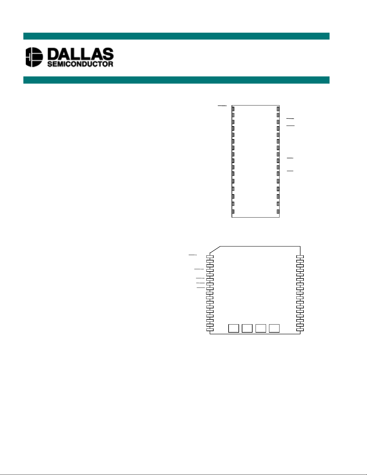
PIN ASSIGNMENT
RST
NC
A14
A12
DQ0
DQ1
DQ2
GND
A7
A6
A5
A4
A3
A2
A1
A0
1
2
3
4
5
6
7
8
9
10
11
12
13
14
15
16
32-Pin Encapsulated Package
1
2
3
4
5
6
7
8
9
10
11
12
13
14
15
16
17
X1 GND
V
BAT
34-Pin PowerCap® Module Board
(Uses DS9034PCX PowerCap)
32
31
30
29
28
27
26
25
24
23
22
21
20
19
18
17
X2
V
CC
NC
IRQ/FT
WE
11
OE
10
CE
DQ7
DQ6
DQ5
DQ4
DQ3
34
33
32
31
30
29
28
27
26
25
24
23
22
21
20
19
18
NC
NC
14
13
12
10
9
7
6
5
4
3
2
1
0
1 of 20 022101
Page 2

ORDERING INFORMATION
DS1554 5V; 32-pin DIP Module
DS1554P 5V; 34-pin PowerCap Module board*
DS1554W 3.3V; 32-pin DIP Module
DS1554WP 3.3V; 34-pin PowerCap Module board*
*DS9034PCX (PowerCap) Required:
must be ordered separately
PIN DESCRIPTION
A0-A14 - Address Input
DQ0-DQ7 - Data Input/Outputs
IRQ \FT - Interrupt, Frequency Test Output
(Open Drain)
RST - Power-On Reset Output
(Open Drain)
CE - Chip Enable
OE - Output Enable
WE - Write Enable
V
CC
GND - Ground
NC - No Connection
X1, X2 - Crystal Connection
V
- Battery Connection
BAT
- Power Supply Input
DS1554
DESCRIPTION
The DS1554 is a full function, year 2000-compliant (Y2KC), real-time clock/calendar (RTC) with a RTC
alarm, watchdog timer, power-on reset, battery monitor, and 32k x 8 non-volatile static RAM. User
access to all registers within the DS1554 is accomplished with a bytewide interface as shown in Figure 1.
The RTC Registers contain century, year, month, date, day, hours, minutes, and seconds data in 24-hour
BCD format. Corrections for day of month and leap year are made automatically.
The RTC Registers are double-buffered into an internal and external set. The use r has direct ac cess to the
external set. Clock/calendar updat es to the external set of re gisters can be disabl ed and enabled to allow
the user to access static data. Assuming the internal oscillator is turned on, the internal set of registers a re
continuously updated; this occurs regardless of external registers settings to guarantee that accurate RTC
information is always maintained.
The DS1554 has interrupt (
The
IRQ /FT interrupt output can be used to generate an external interrupt when the RTC Register values
match user programmed alarm values. The interrupt is always available while the device is powered from
the system supply and can be programmed to occur when in the batter y backed state to serve as a s ystem
wake-up. Either the
IRQ /FT or RST outputs can also be used as a CPU watchdog timer, CPU activity is
monitored and an interrupt or reset output will be activated if the correct activity is not detected within
programmed limits. The DS1554 power-on reset can be used to detect a system power down or failure
and hold the CPU in a safe reset state until normal power returns and stabilizes; the
for this function.
IRQ /FT) and reset (RST ) outputs which can be used to control CPU activity.
RST output is used
2 of 20
Page 3
DS1554
The DS1554 also contains its own power-fail circuitry, which automatically deselects the device when the
VCC supply enters an out of tolerance condition. This feature provides a high degree of data security
during unpredictable system operation brought on by low VCC levels.
PACKAGES
The DS1554 is available in two packages (32-pin DIP and 34-pin PowerCap module). The 32-pin DIP
style module integrates the crystal, lithium energy source, and silicon all in one package. The 34-pin
PowerCap module board is designed with contacts for connection to a separate PowerCap (DS9034PCX)
that contains the crystal and battery. This design allows the PowerCap to be mounted on top of the
DS1554P after the completion of the surface mount process. Mounting the PowerCap aft er the surface
mount process prevents damage to the crystal and battery due to the hi gh tempe ratur es required for solde r
reflow. The PowerCap is keyed to prevent reverse insertion. The PowerCap Module board and PowerCap
are ordered separately and shipped in separate containers. The part number for the PowerCap is
DS9034PCX.
DS1554 BLOCK DIAGRAM Figure 1
DS1554 OPERATING MODES Table 1
V
CC
VCC > V
PF
VSO < VCC <V
VCC <V
SO
< V
CE OE WE
V
IH
V
IL
V
IL
V
IL
PF
PF
X X X HIGH-Z DESELECT CMOS STANDBY
X X X HIGH-Z DATA
X X HIGH-Z DESELECT STANDBY
XVILD
V
V
IL
IH
V
V
DQ0-DQ7 MODE POWER
IN
IH
IH
D
OUT
HIGH-Z READ ACTIVE
WRITE ACTIVE
READ ACTIVE
RETENTION
3 of 20
BATTERY
CURRENT
Page 4

DS1554
DATA READ MODE
The DS1554 is in the read mode whenever CE (chip enable) is low and WE (write enable) is high. The
device architecture allows ripple-through access to any valid address location. Valid data will be available
at the DQ pins within tAA after the last address input is stable, providing that CE and OE access times are
satisfied. If CE or OE access times are not met, valid data will be available at the latter of chip enable
access (t
) or at output enable access time (t
CEA
). The state of the data input/output pins (DQ) is
OEA
controlled by CE and OE . If the outputs are activated before tAA, the data lines are driven to an
intermediate state until tAA. If the address inputs are changed while CE and OE remain valid, output data
will remain valid for output data hold time (tOH ) but will then go indeterminate until the next address
access.
DATA WRITE MODE
The DS1554 is in the write mode whenever WE and CE are in th eir active state. The start of a write is
referenced to the latter occurring transition of WE or CE . The addresses must be held valid throughout
the cycle. CE and WE must return inactive for a minimum of tWR prior to the initiation of a subsequent
read or write cycle. Data in must be valid tDS prior to the end of the write and remain valid for t
afterward. In a typical application, the OE signal will be high during a write cycle. However, OE can be
active provided that care is taken with the data bus to avoid bus contention. If OE is low prior to WE
transitioning low, the data bus can become active with read data defined by the address inputs. A low
transition on WE will then disable the outputs t
after WE goes active.
WEZ
DH
DATA RETENTION MODE
The 5-volt device is fully accessible and data can be written and read only when VCC is greater than VPF.
However, when VCC is below the power-fail point VPF (point at which write protection occurs) the
internal clock registers and SRAM are bl ocked from any acc ess. When VCC falls below the battery switch
point VSO (battery supply level), device power is switched from the VCC pin to the internal backup lithium
battery. RTC operation and SRAM data are maintained from the battery until VCC is returned to nominal
levels.
The 3.3 volt device is fully accessible and data can be written and read only when VCC is greater than VPF.
When VCC falls below VPF, access to the device is inhibited. If VPF is less than VSO, the device power is
switched from VCC to the internal backup lithium battery when VCC drops below VPF. If VPF is greater
than V
below VSO. RTC operation and SRAM data are maintained from the battery until VCC is returned to
nominal levels.
All control, data, and address signals must be powered down when V
, the device power is switched from VCC to the internal backup lithium battery when VCC drops
SO
is powered down.
CC
4 of 20
Page 5

DS1554
BATTERY LONGEVITY
The DS1554 has a lithium power source that is designed to provide energy for the clock activity, and
clock and RAM data retention when the VCC supply is not present. The capability of this internal power
supply is sufficient to power the DS1554 continuously for the life of the equipment in which it is
installed. For specification purposes, the life expectancy is 10 years at 25°C with the internal clock
oscillator running in the absence of VCC. Each DS1554 is shipped from Dallas Semiconductor with its
lithium energy source disconnected, guaranteeing full energy capacity. When V
level greater than V
, the lithium energy source is enabled for battery backup operation. Actual life
PF
is first applied at a
CC
expectancy of the DS1554 will be much longer than 10 years since no internal battery energy is
consumed when VCC is present.
INTERNAL BATTERY MONITOR
The DS1554 constantly monitors the battery voltage of the internal batter. The Battery Low Flag (BLF)
bit of the Flags Register (B4 of 7FFF0h) is not writeable and should always be a 0 when read. If a 1 is
ever present, an exhausted lithium energy source is indicated and both the contents of the RTC and RAM
are questionable.
POWER-ON RESET
A temperature compensated comparator circuit monitors the level of VCC. When VCC falls to the power
fail trip point, the RST signal (open drain) is pulled low. When VCC returns to nominal levels, the
RST signal continues to be pulled low for a period of 40 ms to 200 ms. The power-on reset function is
independent of the RTC oscillator and thus is operational whether or not the oscillator is enabled.
CLOCK OPERATIONS
Table 2 and the following paragraphs describe the operation of RTC, alarm, and watchdog functions.
5 of 20
Page 6
DS1554 REGISTER MAP Table 2
ADDRESS
7FFFh 10 Year YEAR YEAR 00-99
7FFEh X X X 10 M MONTH MONTH 01-12
7FFDh X X 10 Date DATE DATE 01-31
7FFCh X FT X X X DAY DAY 01-07
7FFBh X X 10 HOUR HOUR HOUR 00-23
7FFAh X 10 MINUTES MINUTES MINUTES 00-59
7FF9h
7FF8h W R 10 CENTURY CENTURY CONTROL 00-39
7FF7h WDS BMB4 BMB3 BMB2 BMB1 BMB0 RB1 RB0 WATCHDOG
7FF6h AE Y ABE Y Y Y Y Y INTERRUPTS
7FF5h AM4 Y 10 DATE DATE ALARM DATE 01-31
7FF4h AM3 Y 10 HOURS HOURS ALARM HOURS 00-23
7FF3h AM2 10 MINUTES MINUTES ALARM MINUTES 00-59
7FF2h AM1 10 SECONDS SECONDS ALARM SECONDS 00-59
7FF1h Y Y Y Y Y Y Y Y UNUSED
7FF0h WF AF 0 BLF 0 0 0 0 FLAGS
B
OSC
7
B
6
B
5
10 SECONDS SECONDS SECONDS 00-59
DATA
B
4
B
3
B
B
2
B
1
0
FUNCTION/RANGE
DS1554
X = Unused, read/writeable under Write and Read AE = Alarm Flag Enable
bit control Y = Unused, read/writeable without Write and Read
FT = Frequency Test bit bit control
OSC = Oscillator start/stop bit
ABE = Alarm in battery Back-up mode enable
W = Write bit AM1-AM4 = Alarm Mask bits
R = Read bit WF = Watchdog Flag
WDS = Watchdog Steering bit AF = Alarm Flag
BMB0-BMB4 = Watchdog Multiplier bits 0 = 0 and are read only
RB0-RB1 = Watchdog Resolution bits BLF = Battery Low Flag
CLOCK OSCILLATOR CONTROL
The Clock oscillator may be stopped at any time. To increase the shelf life of the backup lithium battery
source, the oscillator can be turned off to minimize current drain from the battery. The
OSC bit is the
MSB of the Seconds Register (B7 of 7FF9h). Setting it to a 1 stops the oscillator, setting to a 0 starts the
oscillator. The DS1554 is shipped from Dallas Semiconductor with the clock oscillator turned off, OSC
bit set to a 1.
READING THE CLOCK
When reading the RTC data, it is recommended to halt updates to the external set of double-buffered RTC
Registers. This puts the external registers into a static state allowing data to be read without register
values changing during the read process. Normal updates to the internal registers continue while in this
state. External updates are halted when a 1 is written into the read bit, B6 of the Control Register (7FF8h).
As long as a 1 remains in the Control Register read bit, updating is halted. After a halt is issued, the
registers reflect the RTC count (day, date, and time) that was current at the moment the halt command
was issued. Normal updates to the external set of registers will resume within 1 second after the read bit is
set to a 0 for a minimum of 500 µs. The read bit must be a zero for a minimum of 500 µs to ensure the
external registers will be updated.
6 of 20
Page 7

DS1554
SETTING THE CLOCK
The 8th bit, B7 of the Control Register is the write bit. Setting the write bit to a 1, like the read bit, halts
updates to the DS1554 (7FF8h-7FFFh) registers. After setting the write bit to a 1, RTC Registers can be
loaded with the desired RTC count (day, date, and time) in 24-hour BCD format. Setting the write bit to a
0 then transfers the values written to the internal RTC Registers and allows normal operation to resume.
CLOCK ACCURACY (DIP MODULE)
The DS1553 is guaranteed to keep time accuracy to within ±1 minute per month at 25°C. The RTC is
calibrated at the factory by Dallas Semiconductor using nonvolatile tuning elements and does not require
additional calibration. For this reason, methods of field clock calibration are not available and not
necessary. Clock accuracy is also effected by the electrical environment and caution should be taken to
place the RTC in the lowest level EMI section of the PCB layout. For additional information see
application note 58.
CLOCK ACCURACY (POWERCAP MODULE)
The DS1554 and DS9034PCX are each individually tested for accuracy. Once mounted together, the
module is will typically keep time accuracy to within ±1.53 minutes per month (35 ppm) at 25°C. Clock
accuracy is effected by the electrical environment and caution should be taken to place the RTC in the
lowest level EMI section of the PCB layout. For additional information please see application note 58.
FREQUENCY TEST MODE
The DS1554 frequency test mode uses the open drain IRQ /FT output. With the oscillator running, the
IRQ /FT output will toggle at 512 Hz when the FT bit is a 1, the Alarm Flag Enable bit (AE) is a 0, and
the Watchdog Steering bit (WDS) is a 1 or the Watchdog Register is reset (Register 7FF7h = 00h). The
IRQ /FT output and the frequency test mode can be used as a measure of the actual frequency of the
32.768 kHz RTC oscillator. The IRQ/FT pin is an open drain output which requires a pullup resistor for
proper operation. The FT bit is cleared to a 0 on power-up.
USING THE CLOCK ALARM
The alarm settings and control for the DS1554 reside within Registers 7FF2h-7FF5h. Register 7FF6h
contains two alarm enable bits: Alarm Enable (AE) and Alarm in Backup Enable (ABE). The AE and
ABE bits must be set as described below for the
condition.
The alarm can be programmed to activate on a specific day of the month or repeat every day, hour,
minute, or second. It can also be programmed to go off while the DS1554 is in the battery backed state of
operation to serve as a system wake-up. Alarm mask bits AM1-AM4 control the alarm mode. Table 3
shows the possible settings. Configurations not listed in the table default to the once per second mode to
notify the user of an incorrect alarm setting.
IRQ /FT output to be activated for a matched alarm
7 of 20
Page 8

DS1554
ALARM MASK BITS Table 3
AM4 AM3 AM2 AM1 ALARM RATE
1111Once per second
1110When seconds match
1100When minutes and seconds match
1000When hours, minutes, and seconds match
0000When date, hours, minutes, and seconds match
When the RTC Register values match Alarm Register settings, the Alarm Flag bit (AF) is set to a 1. If
Alarm Flag Enable (AE) is also set to a 1, the alarm condition activates th e IRQ /FT pin. The IRQ /FT
signal is cleared by a read or write to the Flags Register (Address 7FF0h) as shown in Figure 2 and 3.
When CE is active, the IRQ /FT signal may be cleared by having the address stabl e for as short as 15 ns
and either OE or WE active, but is not guaranteed to be cleared unless tRC is fulfilled. The alarm flag is
also cleared by a read or write to the Flags Register but the flag will not change states until the end of the
read/write cycle and the IRQ /FT signal has been cleared.
CLEARING IRQ WAVEFORMS Figure 2
CE,
0V
CLEARING IRQ WAVEFORMS Figure 3
CE=0
8 of 20
Page 9
DS1554
The IRQ/FT pin can also be activated in the battery backed mode. The IRQ /FT will go low if an alarm
occurs and both ABE and AE are set. The ABE and AE bits are cleared during the power-up transition,
however an alarm generated during power-up will set AF. Therefore the AF bit can be read after system
power-up to determine if an alarm was generated during the power-up sequence. Figure 4 illustrates alarm
timing during the battery back-up mode and power-up states.
BACK-UP MODE ALARM WAVEFORMS Figure 4
USING THE WATCHDOG TIMER
The watchdog timer can be used to detect an out-of-control processor. The user programs the watchdog
timer by setting the desired amount of time-out into the 8-bit Watchdog Register (Address 7FF7h). The
five Watchdog Register bits BMB4-BMB0 store a binary multiplier and the two lower order bits
RB1-RB0 select the resolution, where 00=1/16 second, 01=1/4 second, 10=1 second, and 11=4 seconds.
The watchdog time-out value is then determined by the multiplication of the 5-bit multiplier value with
the 2-bit resolution value. (For example: writing 00001110 in the Watchdog Register = 3 X 1 second or
3 seconds.) If the processor does not reset the timer within the specified period, the Watchdog Flag (WF)
is set and a processor interrupt is generated and stays active until either the Watchdog Flag (WF) is read
or the Watchdog Register (7FF7) is read or written.
The most significant bit of the Watchdog Register is the Watchdog Steering Bit (WDS). When set to a 0,
the watchdog will activate the IRQ/FT output when the watchdog times out.
When WDS is set to a 1, the watchdog will output a negative pulse on th e RST output for a duration of
40 ms to 200 ms. The Watchdog Register (7FF7) and the FT bit will reset to a 0 at the end of a watchdo g
time-out when the WDS bit is set to a 1.
The watchdog timer resets when the processor performs a read or write of the Watchdog Register. The
time-out period then starts over. The watchdog timer is disabled by writing a value of 00h to the
Watchdog Register. The watchdog function is automatically disabled upon power-up and the Watchdog
Register is cleared. If the watchdog function is set to output to the
function is activated, the watchdog function prevails and the frequency test function is denied.
IRQ /FT output and the frequency test
POWER-ON DEFAULT STATES
Upon application of power to the device, the following register bits are set to a 0:
WDS=0, BMB0-BMB4=0, RB0-RB1=0, AE=0, ABE=0.
9 of 20
Page 10

DS1554
ABSOLUTE MAXIMUM RATINGS*
Voltage on Any Pin Relative to Ground -.3V to +6.0V
Storage Temperature -55°C to +125°C
Soldering Temperature 260°C for 10 seconds (DIP Package) (See Note 8)
See IPC/JEDEC Standard J-STD-020A for
Surface Mount Devices
* This is a stress rating only and functional operation of the device at these or an y other conditions above
those indicated in the operation sections of this specification is not implied. Exposure to absolute
maximum rating conditions for extended periods of time may affect reliability.
OPERATING RANGE
Range Temperature V
Commercial 0°C to +70°C
3.3V ± 10% or 5V ± 10%
CC
RECOMMENDED DC OPERATING CONDITIONS (Over the Operating Range)
PARAMETER SYMBOL MIN TYP MAX UNITS NOTES
Logic 1 Voltage All Inputs
VCC = 5V ±10%
VCC = 3.3V ±10%
Logic 0 Voltage All Inputs
VCC = 5V ±10% V
VCC = 3.3V ±10%
V
V
V
IH
IH
IL
IL
2.2 VCC +0.3V V 1
2.0 VCC +0.3V V 1
-0.3 0.8 1
-0.3 0.6 1
DC ELECTRICAL CHARACTERISTICS
(Over the Operating Range; V
PARAMETER SYMBOL MIN TYP MAX UNITS NOTES
Active Supply Current I
TTL Standby Current (CE =VIH )
CMOS Standby Current
CE ≥=V
(
– 0.2V)
CC
I
I
Input Leakage Current (any input) I
Output Leakage Current (any
output)
Output Logic 1 Voltage
= -1.0 mA)
(I
OUT
V
Output Logic 0 Voltage
= 2.1 mA, DQ0-7 Outputs) V
(I
OUT
(I
= 7.0 mA, IRQ /FT and RST
OUT
V
outputs)
Write Protection Voltage V
Battery Switch Over Voltage V
CC
CC1
CC2
I
OL
OL1
OL2
IL
OH
PF
SO
-1 +1
-1 +1
2.4 V 1
4.25 4.50 V 1
40 75 mA 2, 3
3 6 mA 2, 3
2 4 mA 2, 3
0.4 V 1
0.4 V 1, 5
V
BAT
=5.0V ±10%)
CC
µA
µA
V 1, 4
10 of 20
Page 11

DC ELECTRICAL CHARACTERISTICS
DS1554
(Over the Operating Range; V
=3.3V ±10%)
CC
PARAMETER SYMBOL MIN TYP MAX UNITS NOTES
Active Supply Current I
TTL Standby Current (CE = VIH )
CMOS Standby Current
I
I
CC
CC1
CC2
10 30 mA 2, 3
0.7 3 mA 2, 3
0.7 2 mA 2, 3
(CE ≥=VCC - 0.2V)
Input Leakage Current (any input) I
Output Leakage Current
IL
I
OL
-1 +1
-1 +1
µA
µA
(any output)
Output Logic 1 Voltage
(I
= -1.0 mA)
OUT
V
OH
2.4 V 1
Output Logic 0 Voltage
(I
=2.1 mA, DQ0-7 Outputs) V
OUT
(I
=7.0 mA, IRQ /FT and RST
OUT
V
OL1
OL2
0.4 V 1
0.4 V 1, 5
Outputs)
Write Protection Voltage V
Battery Switch Over Voltage V
PF
SO
2.80 2.97 V 1
V
BAT
V
or
PF
V 1, 4
READ CYCLE TIMING DIAGRAM Figure 5
11 of 20
Page 12

DS1554
READ CYCL E, AC CHARACTERISTICS (Over the Operating Range)
VCC=5.0V ±±±±10% VCC=3.3V ±±±±10%
PARAMETER SYMBOL
Read Cycle Time t
Address Access Time t
CE to DQ Low-Z
CE Access Time
CE Data Off time
OE to DQ Low-Z
OE Access Time
OE Data Off Time
Output Hold from Address t
t
t
t
t
t
OEA
t
OEZ
RC
AA
CEL
CEA
CEZ
OEL
OH
MIN MAX MIN MAX
UNITS NOTES
70 120 ns
70 120 ns
55ns
70 120 ns
25 40 ns
55ns
35 100 ns
25 35 ns
55ns
WRITE CYCLE, AC CHARACTERISTICS (Over the Operating Range)
VCC=5.0V ±±±±10% VCC=3.3V ±±±±10%
PARAMETER SYMBOL
Write Cycle Time t
Address Access Time t
WE Pulse Width
CE Pulse Width
Data Setup Time t
Data Hold time t
Data Hold time t
Address Hold Time t
Address Hold Time t
WE Data Off Time
Write Recovery Time t
WC
AS
t
WEW
t
CEW
DS
DH1
DH2
AH1
AH2
t
WEZ
WR
MIN MAX MIN MAX
UNITS NOTES
70 120 ns
00ns
50 100 ns
60 110 ns
30 80 ns
0 0 ns 9
0 5 ns 10
5 0 ns 9
5 5 ns 10
25 40 ns
510ns
12 of 20
Page 13

WRITE CYCLE TIMING, WRITE ENABLE CONTROLLED Figure 6
DS1554
WRITE CYCLE TIMING, CHIP ENABLE CONTROLLED Figure 7
13 of 20
Page 14

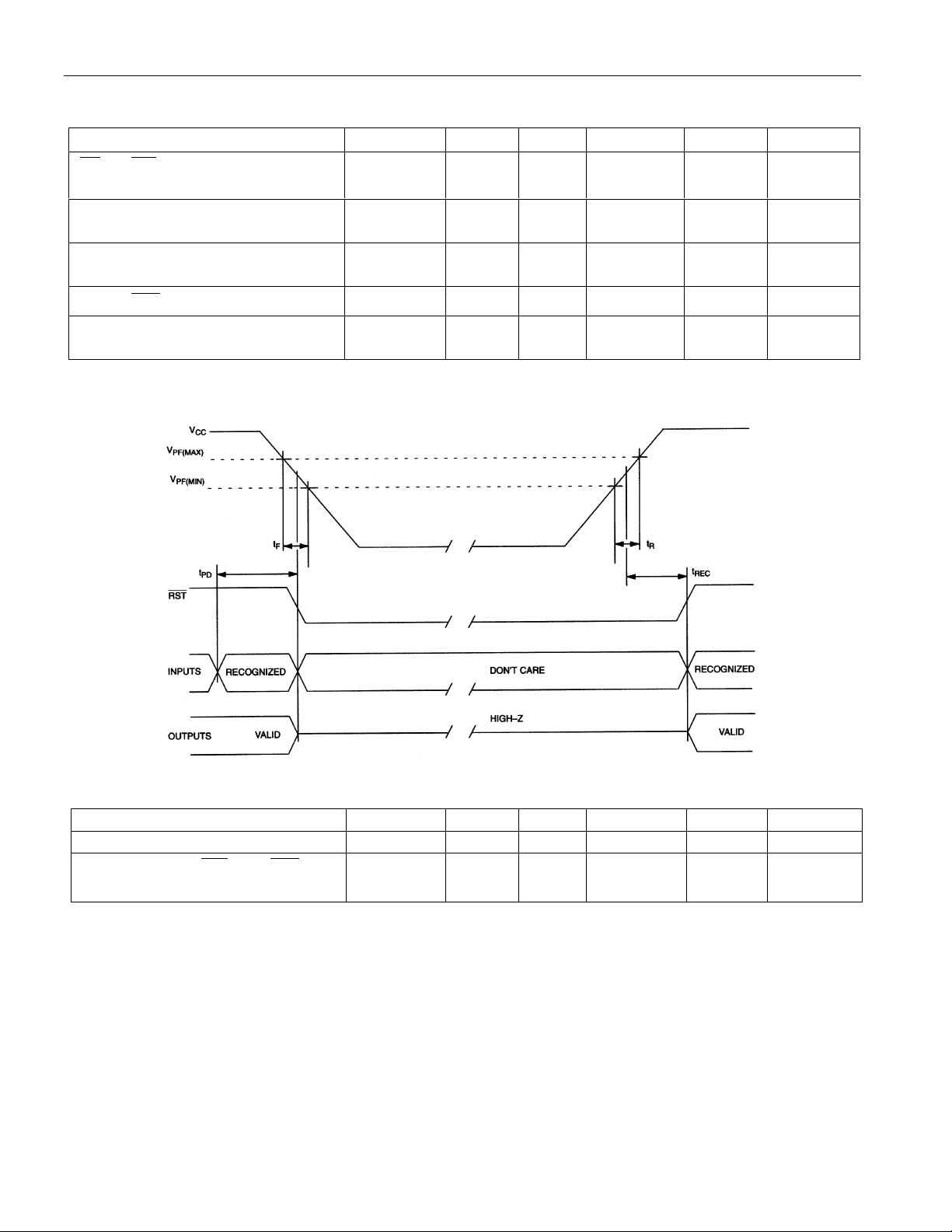
POWER-UP/DOWN CHARACTERISTICS
DS1554
(Over the Operating Range; V
=5.0V ±10%)
CC
PARAMETER SYMBOL MIN TYP MAX UNITS NOTES
CE or WE at V
Power-Down
VCC Fall Time: V
V
PF(MIN)
VCC Fall Time: V
VCC Rise Time: V
V
PF(MAX)
VPF to RST High
Expected Data Retention Time
(Oscillator On)
, Before
IH
PF(MAX)
PF(MIN)
PF(MIN)
to
to V
to
SO
t
t
t
REC
t
t
FB
t
DR
PD
R
0
F
300
10
0
µs
µs
µs
µs
40 200 ms
10 years 6, 7
POWER-UP/DOWN WAVEFORM TIMING 5-VOLT DEVICE Figure 8
14 of 20
Page 15
POWER-UP/DOWN CHARACTERISTICS
DS1554
(Over the Operating Range; V
=3.3V ±10%)
CC
PARAMETER SYMBOL MIN TYP MAX UNITS NOTES
CE or WE at V
Power-Down
VCC Fall Time: V
V
PF(MIN)
VCC Rise Time: V
V
PF(MAX)
VPF to RST High
Expected Data Retention Time
(Oscillator On)
, Before
IH
PF(MAX)
PF(MIN)
to
to
t
t
REC
t
PD
t
t
DR
0
F
R
300
0
µs
µs
µs
40 200 ms
10 years 6, 7
POWER-UP/DOWN WAVEFORM TIMING 3.3-VOLT DEVICE Figure 9
CAPACITANCE (TA = 25°C)
PARAMETER SYMBOL MIN TYP MAX UNITS NOTES
Capacitance on all input pins C
Capacitance on IRQ /FT, RST ,
C
and DQ pins
IN
IO
15 of 20
7pF1
10 pF 1
Page 16

AC TEST CONDITIONS
Output Load: 100 pF + 1TTL Gate
Input Pulse Levels: 0.0 to 3.0V
Timing Measurement Reference Levels:
Input: 1.5V
Output: 1.5V
Input Pulse Rise and Fall Times: 5 ns
NOTES:
1. Voltage referenced to ground.
2. Typical values are at 25°C and nominal supplies.
3. Outputs are open.
4. Battery switch over occurs at the lower of either the battery voltage or VPF.
5. The IRQ /FT and RST outputs are open drain.
6. Data retention time is at 25°C.
DS1554
7. Each DS1554 has a built-in switch that disconnects the lithium source until VCC is first applied by the
user. The expected tDR is defined for DIP modules and PowerCap modules as a cumulative time in
the absence of VCC starting from the time power is first applied by the user.
8. Real Time Clock Modules (DIP) can be successfully processed through conventional wave-soldering
techniques as long as temperature exposure to the lithium energy source contained within does not
exceed +85°C. Post solder cleaning with water washing techniques is acceptable, provided that
ultrasonic vibration is not used.
In addition, for the PowerCap:
a. Dallas Semiconductor recommends that PowerCap Module bases experience one pass through
solder reflow oriented with the label side up (“live-bug”).
b. Hand soldering and touch-up: Do not touch or apply the soldering iron to leads for more than
3 seconds. To solder, apply flux to the pad, heat the lead frame pad and apply solder. To remove
the part, apply flux, heat the lead frame pad until the solder reflow and use a solder wick to
remove solder.
, t
9. t
10. t
AH1
AH1
are measured from WE going high.
DH1
, t
are measured from CE going high.
DH1
16 of 20
Page 17
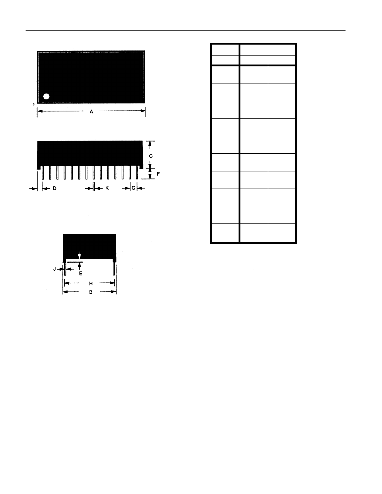
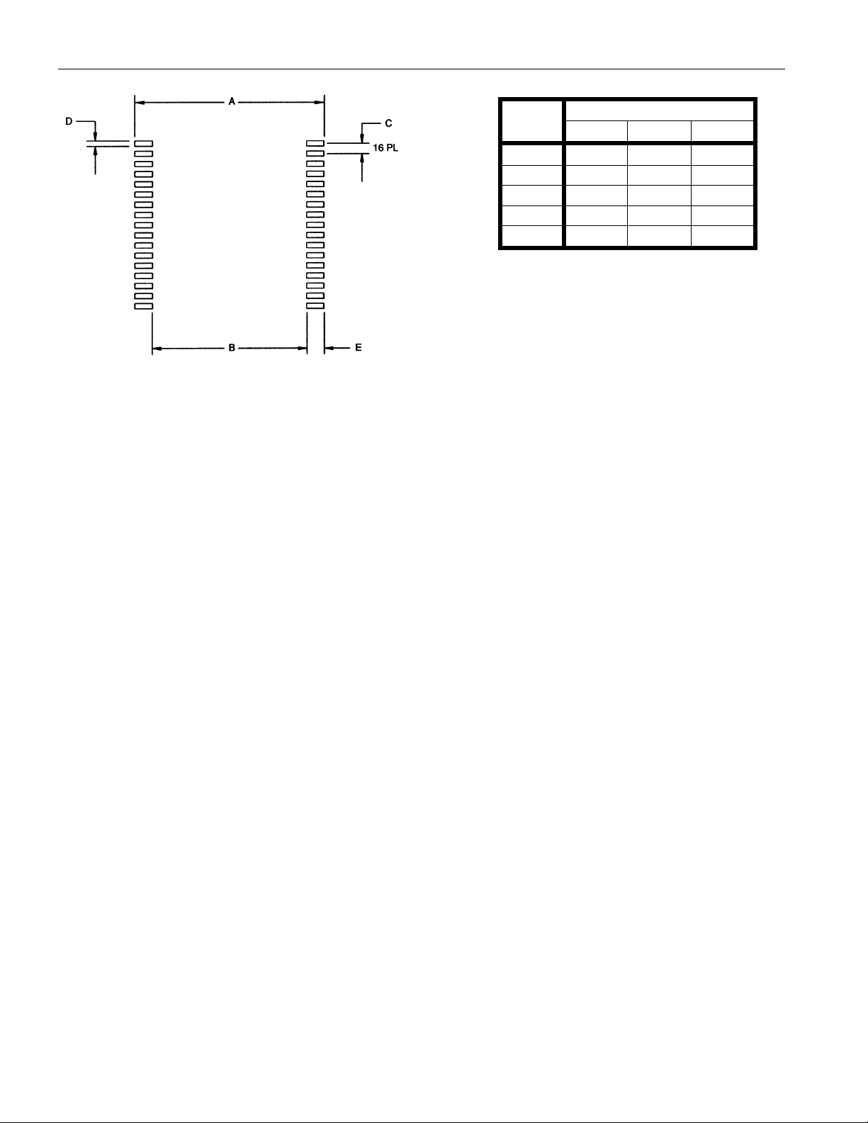
DS1554 32-PIN PACKAGE
PKG 32-PIN
DIM MIN MAX
A IN.
MM
B IN.
MM
C IN.
MM
D IN.
MM
E IN.
MM
F IN.
MM
G IN.
MM
H IN.
MM
J IN.
MM
K IN.
MM
1.670
38.42
0.715
18.16
0.335
8.51
0.075
1.91
0.015
0.38
0.140
3.56
0.090
2.29
0.590
14.99
0.010
0.25
0.015
0.38
1.690
38.93
0.740
18.80
0.365
9.27
0.105
0.67
0.030
0.76
0.180
4.57
0.110
2.79
0.630
16.00
0.018
0.45
0.025
0.64
DS1554
17 of 20
Page 18
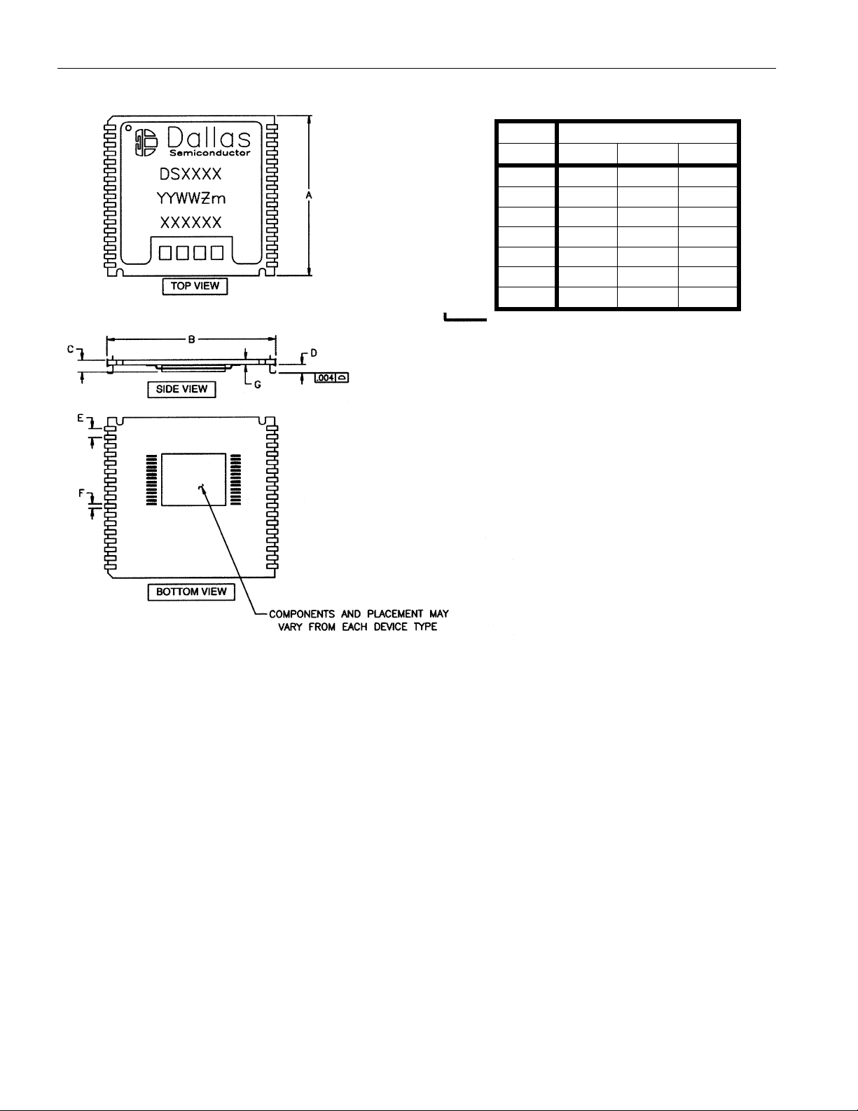
DS1554P
PKG INCHES
DIM MIN NOM MAX
A
B
C
D
E
F
G
0.920 0.925 0.930
0.980 0.985 0.990
- - 0.080
0.052 0.055 0.058
0.048 0.050 0.052
0.015 0.020 0.025
0.025 0.027 0.030
DS1554
NOTE:
Dallas Semiconductor recommends that PowerCap Module bases experience one pass through solder
reflow oriented with the label side up (“live-bug”).
Hand Soldering and touch-up: Do not touch or apply the soldering iron to leads for more than 3 seconds.
To solder, apply flux to the pad, heat the lead frame pad and apply solder. To remove the part, apply flux,
heat the lead frame pad until the solder reflows and use a solder wick to remove solder.
18 of 20
Page 19
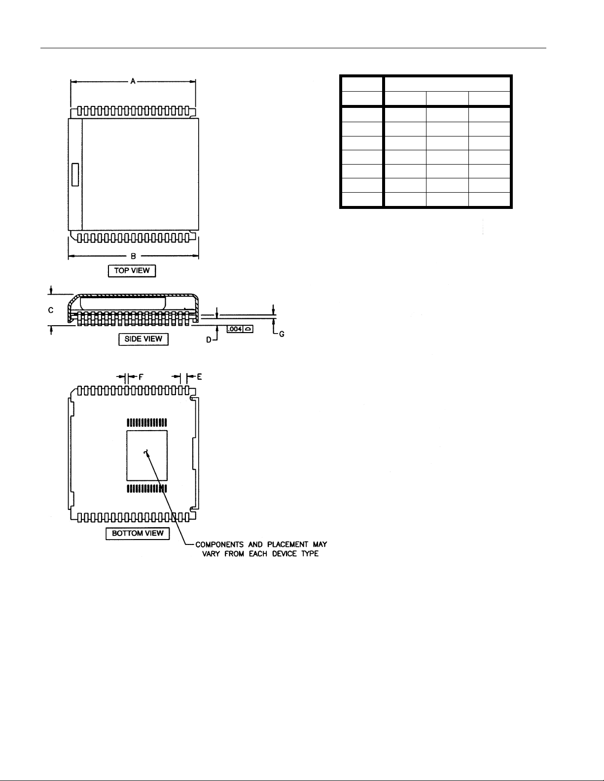
DS1554P WITH DS9034PCX ATTACHED
PKG INCHES
DIM MIN NOM MAX
A
B
C
D
E
F
G
0.920 0.925 0.930
0.955 0.960 0.965
0.240 0.245 0.250
0.052 0.055 0.058
0.048 0.050 0.052
0.015 0.020 0.025
0.020 0.025 0.030
DS1554
19 of 20
Page 20
RECOMMENDED POWERCAP MODULE LAND PATTERN
DS1554
PKG
DIM
A
B
C
D
E
INCHES
MIN NOM MAX
- 1.050 -
- 0.826 -
- 0.050 -
- 0.030 -
- 0.112 -
20 of 20
 Loading...