

Page 1
WE
KS
CE
A
A3A
A
A
PWR
R
IRQ
Y2K Watchdog Real-Time Clocks
www.maxim-ic.com
GENERAL DESCRIPTION
The DS1501/DS1511 are full-function, year 2000compliant real-time clock/calendars (RTCs) with an
RTC alarm, watchdog timer, power-on reset, battery
monitors, 256 bytes NV SRAM, and a 32.768kHz
output. User access to all registers within the
DS1501/DS1511 is accomplished with a byte-wide
interface, as shown in Figure 8. The RTC registers
contain century, year, month, date, day, hours,
minutes, and seconds data in 24-hour binary-coded
decimal (BCD) format. Corrections for day of month
and leap year are made automatically.
APPLICATIONS
Remote Systems
Battery-Backed Systems
Telecom Switches
Office Equipment
Consumer Electronics
ORDERING INFORMATION
PART TEMP RANGE PIN-PACKAGE
DS1501YN
DS1501YEN -40°C to +85°C 28 TSOP
DS1501YSN -40°C to +85°C 28 SO (330 mil)
DS1501WN -40°C to +85°C 28 DIP (600 mil)
DS1501WEN -40°C to +85°C 28 TSOP
DS1501WSN -40°C to +85°C 28 SO (330 mil)
DS1511Y
DS1511W 0°C to +70°C 28 720-mil Module
Selector Guide appears at end of data sheet.
Typical Operating Circuits appears at end of data sheet.
-40°C to +85°C 28 DIP (600 mil)
0°C to +70°C 28 720-mil Module
FEATURES
§ BCD-Coded Century, Year, Month, Date, Day,
Hours, Minutes, and Seconds with Automatic
Leap-Year Compensation Valid Up to the Year
2100
§ Programmable Watchdog Timer and RTC Alarm
§ Century Register; Y2K-Compliant RTC
§ Automatic Battery Backup and Write Protection
to External SRAM
§ +3.3 or +5V Operation
§ Precision Power-On Reset
§ Power-Control Circuitry Support System Power-
On from Date/Day/Time Alarm or Key
Closure/Modem-Detect Signal
§ 256 Bytes Battery-Backed NV SRAM
§ Auxiliary Battery Input
§ Accuracy of DS1511 Better than ±1
Minute/Month at +25°C
§ Day-of-Week/Date Alarm Register
§ Crystal Select Bit Allow RTC to Operate with 6pF
or 12.6pF Crystal
§ Battery Voltage-Level Indicator Flags
§ Available as Chip (DS1501) or Standalone
Module with Embedded Battery and Crystal
(DS1511)
§ UL Recognized
PIN CONFIGURATION
TOP VIEW
X1
X2
ST
4
2
1
0
DQ0
DQ1
DQ2
GND
DS1501/DS1511
1
2
3
4
Dallas
5
Semiconductor
DS1501
6
7
8
9
10
11
12
13
14
28
V
27
26
25
24
23
22
21
20
19
18
17
16
15
CC
V
BAUX
V
BAT
SQW
OE
GND
DQ7
DQ6
DQ5
DQ4
DQ3
DIP, SO
Pin Configurations are continued at end of data sheet.
Note: Some revisions of this device may incorporate deviations from published specifications known as errata. Multiple revisions of any device
may be simultaneously available through various sales channels. For information about device errata, click here: www.maxim-ic.com/errata
.
1 of 20
REV: 030603
Page 2

DS1501/DS1511 Y2KC Watchdog Real-Time Clocks
ABSOLUTE MAXIMUM RATINGS
Voltage Range on Any Pin Relative to Ground -0.5V to +6.0V
Operating Temperature Range (Module) 0°C to +70°C
Operating Temperature Range, DS1501
-40°C to +85°C (Note 1)
Operating Temperature Range, DS1511 0°C to +70°C
Storage Temperature Range, DS1501
-55°C to +125°C
Storage Temperature Range, DS1511 -40°C to +70°C
Soldering Temperature (DIP, Module) +260°C Lead Temperature for 10 seconds (max) (Note 2)
Soldering Temperature (SO, TSOP)
Stresses beyond those listed under “Absolute Maximum Ratings” may cause permanent damage to the device. These are stress ratings only,
and functional operation of the device at these or any other conditions beyond those indicated in the operational sections of the specifications is
not implied. Exposure to the absolute maximum rating conditions for extended periods may affect device.
See IPC/JEDEC J-STD-020A for Surface Mount Devices
RECOMMENDED DC OPERATING CONDITIONS
(VCC = 3.3V or 5V ±10%, TA = 0°C to +70°C; VCC = 3.3V or 5V ±10%, TA = -40°C to +85°C.)
PARAMETER SYMBOL CONDITIONS MIN TYP MAX UNITS
Power Supply Voltage (Note 3) VCC
Logic 1 Voltage All Inputs (Note 3) VIH
Pullup Voltage, IRQ, PWR, and
RST Outputs (Note 3)
V
PU
Logic 0 Voltage All Inputs (Note 3) VIL
Battery Voltage (Note 3) V
Auxiliary Battery Voltage (Note 3) V
BAT
BAUX
5V (Y) 4.5 5.0 5.5
3.3V (W) 3.0 3.3 3.6
Y 2.2 VCC + 0.3
W 2.0 V
+ 0.3
CC
V
V
5.5 V
Y -0.3 +0.8
W -0.3 +0.6
V
2.5 3.0 3.7 V
Y 2.5 3.0 5.3
W 2.5 3.0 3.7
V
DC ELECTRICAL CHARACTERISTICS
(VCC = 3.3V or 5V ±10%, TA = 0°C to +70°C; VCC = 3.3V or 5V ±10%, TA = -40°C to +85°C.)
PARAMETER SYMBOL CONDITIONS MIN TYP MAX UNITS
Active Supply Current (Note 4) ICC
I
(
CE = V
)
IH
CMOS Standby Current
(
CE = V
- 0.2V)
CC
CC1
I
CC2
Input Leakage Current (Any Input) IIL -1 +1
Output Leakage Current
(Any Output)
Output Logic 1 Voltage
= -1.0mA)
(I
OUT
Output Logic 0 Voltage (I
2.1mA, DQ0–7; I
I
= 7.0mA, PWR and RST )
OUT
= 5.0mA, IRQ,
OUT
(Note 2)
OUT
=
I
OL
V
OH
V
OL1
V
OL2
V
BLF
Power-Fail Voltage (Note 2) VPF
Battery Switchover Voltage
(Notes 3, 6)
V
SO
Y 15
W 10
Y 5 TTL Standby Current
W 4
Y 5
W 4
mA
mA
mA
mA
-1 +1
mA
(Note 3) 2.4 V
(Note 3) 0.4 V
(Notes 3, 5) 0.4 V
Y 2.0 Battery Low, Flag Trip Point
W 1.9
Y 4.20 4.50
W 2.75 2.97
V
BAT,
V
BAUX,
or V
PF
V
V
V
2 of 20
Page 3

DS1501/DS1511 Y2KC Watchdog Real-Time Clocks
PARAMETER SYMBOL CONDITIONS MIN TYP MAX UNITS
Battery Leakage Current I
100 nA
LKG
DC ELECTRICAL CHARACTERISTICS
(VCC = 0V; TA = 0°C to +70°C; VCC = 0V, TA = -40°C to +85°C.)
PARAMETER SYMBOL CONDITIONS MIN TYP MAX UNITS
Battery Current, BB32 = 0, EOSC = 0
Battery Current, BB32 = 0, EOSC = 1
V
Current BB32 = 1, SQW Open I
BAUX
BAT1
I
BAT2
BAUX
(Note 7)
(Note 7)
(Note 7) 2 µA
0.27 1.0 µA
0.01 0.1 µA
I
CRYSTAL SPECIFICATIONS*
PARAMETER SYMBOL CONDITIONS MIN TYP MAX UNITS
Nominal Frequency fO 32.768 kHz
Series Resistance ESR 45 kΩ
Load Capacitance CL 6 pF
*The crystal, traces, and crystal input pins should be isolated from RF generating signals. Refer to Application Note 58: Crystal Considerations
for Dallas Real-Time Clocks for additional specifications.
AC OPERATING CHARACTERISTICS
(VCC = 5V ±10%, TA = 0°C to +70°C; VCC = 5V ±10%, TA = -40°C to +85°C.)
PARAMETER SYMBOL CONDITIONS MIN TYP MAX UNITS
Read Cycle Time tRC
Address Access Time tAA
CE to DQ Low-Z
CE Access Time
CE Data Off Time
OE to DQ Low-Z (0°C to +85°C)
OE to DQ Low-Z (-40°C to 0°C)
OE Access Time
OE Data Off Time
Output Hold from Address tOH
Write Cycle Time
Address Setup Time
WE Pulse Width
CE Pulse Width
Data Setup Time
Data Hold Time
Address Hold Time
WE Data Off Time
Write Recovery Time
Pulse Width, OE, WE, or CE High
Pulse Width, OE, WE, or CE Low
PW
PW
t
t
t
t
t
t
t
CEL
CEA
CEZ
OEL
OEL
OEA
OEZ
(Note 8)
(Note 8)
(Note 8)
(Note 8)
(Note 8)
70 ns
t
WC
0 ns
t
AS
t
50 ns
WEW
t
55 ns
CEW
30 ns
t
DS
t
5 ns
DH
0 ns
t
AH
t
(Note 8) 25 ns
WEZ
t
15 ns
WR
20 ns
HIGH
70 ns
LOW
70 ns
70 ns
5 ns
70 ns
25 ns
5 ns
2 ns
35 ns
25 ns
5 ns
3 of 20
Page 4
DS1501/DS1511 Y2KC Watchdog Real-Time Clocks
OE C
AC OPERATING CHARACTERISTICS
(VCC = 3.3V ±10%, TA = 0°C to +70°C; VCC = 3.3V ±10%, TA = -40°C to +85°C.)
PARAMETER SYMBOL CONDITIONS MIN TYP MAX UNITS
Read Cycle Time
Address Access Time
CE to DQ Low-Z
CE Access Time
CE Data Off Time
OE to DQ Low-Z (0°C to +85°C)
OE to DQ Low-Z (-40°C to 0°C)
OE Access Time
OE Data Off Time
Output Hold from Address
Write Cycle Time
Address Setup Time
WE Pulse Width
CE Pulse Width
Data Setup Time
Data Hold Time
Address Hold Time
WE Data Off Time
Write Recovery Time
Pulse Width, OE, WE, or CE High
Pulse Width, OE, WE, or CE Low
Figure 1. Read Cycle Timing
120 ns
t
RC
120 ns
t
AA
t
(Note 8) 5 ns
CEL
t
120 ns
CEA
t
(Note 8) 40 ns
CEZ
t
(Note 8) 5 ns
OEL
t
(Note 8) 2 ns
OEL
t
100 ns
OEA
t
(Note 8) 35 ns
OEZ
5 ns
t
OH
120 ns
t
WC
0 ns
t
AS
t
100 ns
WEW
t
110 ns
CEW
80 ns
t
DS
5 ns
t
DH
5 ns
t
AH
t
(Note 8) 40 ns
WEZ
15 ns
t
WR
PW
PW
40 ns
HIGH
100 ns
LOW
t
RC
A0–A4
E
DQ0-DQ7
t
t
AA
t
CEA
t
CEL
t
OEA
t
OEL
VALID
t
OEZ
OH
t
CEZ
4 of 20
Page 5
DS1501/DS1511 Y2KC Watchdog Real-Time Clocks
WE C
WE C
Figure 2. Write Cycle Timing, Write-Enable-Controlled
t
WC
A0–A4
VALID VALID
t
AS
t
AH
E
t
AS
t
WEW
DQ0–DQ7
DATA OUTPUT DATA INPUT
t
WEZ
t
DS
DATA INPUT
t
DH
Figure 3. Write Cycle Timing, Chip-Enable-Controlled
t
WR
A0–A4
E
DQ0–DQ7
t
WC
VALID VALID
t
AS
t
AS
t
CEW
t
DS
DATA INPUT
t
AH
t
WR
t
DH
DATA INPUT
5 of 20
Page 6
Figure 4. Burst Mode Timing Waveform
O
DS1501/DS1511 Y2KC Watchdog Real-Time Clocks
A0–A4
E, WE, OR CE
DQ0–DQ7
13h
LOW
PW
HIGH
PW
POWER-UP/DOWN CHARACTERISTICS
PARAMETER SYMBOL CONDITIONS MIN TYP MAX UNITS
CE or WE at V
IH
VCC Fall Time: V
VCC Fall Time: V
VCC Rise Time: V
VPF to RST High
t
t
REC
PF
FB
F
R
Before Power-Fail
to V
PF(MAX)
to VSO t
PF(MIN)
to V
PF(MIN)
t
PF(MIN)
t
PF(MAX)
0
300
10
0
ms
ms
ms
ms
35 200 ms
(TA = +25°C)
PARAMETER SYMBOL CONDITIONS MIN TYP MAX UNITS
Expected Data Retention Time
(Oscillator On)
t
(Note 9) 10 years
DR
CAPACITANCE
(TA = +25°C)
PARAMETER SYMBOL CONDITIONS MIN TYP MAX UNITS
Capacitance on All Input Pins CIN 10 pF
Capacitance on IRQ, PWR, RST, and DQ
Pins
10 pF
C
IO
AC TEST CONDITIONS
OUTPUT LOAD
(Y) 50pF + 1TTL Gate Input: 1.5V
(W) 25pF + 1 TTL Gate
INPUT PULSE
LEVELS
0V to 3.0V for 5V
operation
TIMING MEASUREMENT
REFERENCE LEVELS
Output: 1.5V
6 of 20
INPUT PULSE RISE
AND FALL TIMES
5ns
Page 7
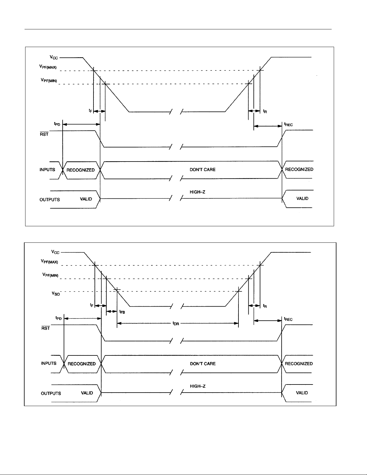
Figure 5. 3.3V Power-Up/Down Waveform Timing
DS1501/DS1511 Y2KC Watchdog Real-Time Clocks
Figure 6. 5V Power-Up/Down Waveform Timing
Warning: Under no circumstances are negative undershoots, of any amplitude, allowed when device is in battery-
backup mode.
7 of 20
Page 8

DS1501/DS1511 Y2KC Watchdog Real-Time Clocks
WAKEUP/KICKSTART TIMING
(TA = +25°C) (Figure 7)
PARAMETER SYMBOL
Kickstart-Input Pulse Width t
Wakeup/Kickstart Power-On Timeout t
KSPW
POTO
Note: Time intervals shown above are referenced in Wakeup/Kickstart.
Figure 7. Wakeup/Kickstart Timing Diagram
V
CO NDIT ION :
<
V
PFVBAT
CO NDIT ION :
VPF>
BAT
V
PF
0V
V
CC
V
PF
V
BAT
V
BAT
0V
V
CC
t
POTO
CONDITIONS
2
(Note 10) 2 s
MIN TYP MAX UNITS
ms
TDF/KSF
(INTE R NA L)
t
KSPW
V
IH
___
KS
V
IL
V
IH
____
PW R
HI-Z
V
IL
V
IH
____
IRQ
HI-Z
V
IL
INT E R VA LS
1
2
3
4
5
Note 1: Limits at -40°C are not production tested and are guaranteed by design.
Note 2: RTC modules can be successfully processed through conventional wave-soldering techniques as long as temperature exposure to the
lithium energy source contained within does not exceed +85°C. Post-sold cleaning with water-washing techniques is acceptable,
provided that ultrasonic vibration is not used to prevent damage to the crystal.
Note 3: Voltage referenced to ground.
Note 4: Outputs are open.
Note 5: The IRQ, PWR, and RST outputs are open drain.
Note 6: If V
is greater than V
of V
Note 7: V
is less than V
PF
or V
BAT
or V
BAT
BAUX
current. Using a 32,768Hz crystal connected to X1 and X2.
BAUX
.
BAT
and V
BAT
and V
, the device power is switched from VCC to the greater of V
BAUX
, the device power is switched from VCC to the greater of V
BAUX
BAT
BAT
or V
or V
when VCC drops below VPF. If VPF
BAUX
when VCC drops below the greater
BAUX
Note 8: These parameters are sampled with a 5pF load and are not 100% tested.
Note 9: t
Note 10: If the oscillator is not enabled, the startup time of the oscillator after V
is the amount of time that the internal battery can power the internal oscillator and internal registers of the DS1511.
DR
is applied will be added to the wakeup/kickstart timeout.
CC1
Note 11: Typical values are at +25°C, nominal (active) supply, unless otherwise noted.
8 of 20
Page 9

DS1501/DS1511 Y2KC Watchdog Real-Time Clocks
PIN DESCRIPTION
PIN
DIP, SO MODULE TSOP
1 1 8
2, 3 — 9, 10 X1, X2
4 4 11
5 5 12
6–10 6–10 13–17 A4–A0 Address Inputs. Selects one of 17 register locations.
11–13,
15–19
11–13,
15–19
18–20,
22–26
14, 21 14 21, 28 GND
22 22 1
20 20 27
23 23 2 SQW
24 24 3
25 — 4 V
26 26 5 V
27 27 6
28 28 7 VCC
—
*See “Conditions of Acceptability” at www.maxim-ic.com/TechSupport/QA/ntrl.htm.
2, 3, 21,
25
— N.C. No Connect
NAME FUNCTION
Power-On Output (Open Drain). This output, if used, is normally connected to
PWR
power-supply control circuitry. This pin requires a pullup resistor connected to a
positive supply to operate correctly.
Connections for a standard 32.768kHz quartz crystal. For greatest accuracy, the
DS1501 must be used with a crystal that has a specified load capacitance of either
6pF or 12.5pF. The crystal select (CS) bit in control register B is used to select
operation with a 6pF or 12.5pF crystal. The crystal is attached directly to the X1 and
X2 pins. There is no need for external capacitors or resistors. An external 32.768kHz
oscillator can also drive the DS1501. In this configuration, the X1 pin is connected to
the external oscillator signal and the X2 pin is floated. For more information about
crystal selection and crystal layout considerations, refer to Application Note 58:
Crystal Considerations with Dallas Real-Time Clocks. See Figure 9. An enable bit in
the month register controls the oscillator. Oscillator startup time is highly dependent
upon crystal characteristics, PC board leakage, and layout. High ESR and excessive
capacitive loads are the major contributors to long startup times. A circuit using a
crystal with the recommended characteristics and proper layout usually starts within
one second.
Reset Output (Open Drain). This output, if used, is normally connected to a
RST
microprocessor-reset input. This pin requires a pull up resistor connected to a
positive supply to operate correctly. When RST is active, the device is not
accessible.
Interrupt Output (Open Drain). This output, if used, is normally connected to a
IRQ
microprocessor interrupt input. This pin requires a pullup resistor connected to a
positive supply to operate correctly.
DQ0–DQ7 Data I/O pins for 8-bit parallel data transfer.
DC power is applied to the device on these pins. V
power is applied within the normal limits, the device is fully accessible and data can
be written and read. When V
inhibited. As V
drops below the battery voltage, the RAM and timekeeping circuits
CC
drops below the normal limits, reads and writes are
CC
are switched over to the battery.
OE
CE
Output-Enable Input. Active-low input that enables DQ0–DQ7 for data output from
the device.
Chip-Enable Input. Active-low input to enable the device.
Square-Wave Output. When enabled, the SQW pin outputs a 32.768kHz square
wave. If the square wave (E32K) and battery backup 32kHz (BB32) bits are enabled,
power is provided by V
when VCC is absent.
BAUX
Kickstart Input. This pin is used to wake up a system from an external event, such
KS
as a key closure. The KS pin is normally connected using a pullup resistor to V
If the KS function is not used, connect to ground.
Battery input for any standard 3V lithium cell or other energy source. Battery voltage
BAT
against reverse charging current when used with a lithium battery. If not used,
must be held between 2.5V and 3.7V for proper operation. UL recognized to ensure
connect to ground.*
Auxiliary battery input for any standard 3V lithium cell or other energy source.
BAUX
recognized to ensure against reverse charging current when used with a lithium
Battery voltage must be held between 2.5V and 3.7V for proper operation. UL
battery. If not used, connect to ground.*
WE
Write-Enable Input. Active-low input that enables DQ0–DQ7 for data input to the
device.
DC power is applied to the device on these pins. V
power is applied within the normal limits, the device is fully accessible and data can
be written and read. When V
inhibited. As V
drops below the battery voltage, the RAM and timekeeping circuits
CC
drops below the normal limits, reads and writes are
CC
are switched over to the battery.
is the positive terminal. When
CC
is the positive terminal. When
CC
BAUX
.
9 of 20
Page 10
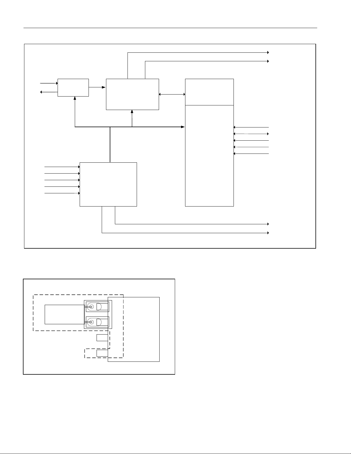
Figure 8. Block Diagram
R
P
K
CE WE O
I
X1
X2
32.768kHz CLOCK
OSCILLATOR
CLOCK ALARM AND WATCHDOG
COUNTDOWN
V
BAT
V
BAT
V
BAUX
GND
S
POWER CONTROL
WRITE PROTECTION,
AND POWER-ON
RESET
Figure 9. Typical Crystal Layout
LOCAL GROUND PLANE (LAYER 2)
DS1501/DS1511 Y2KC Watchdog Real-Time Clocks
RQ
SQW
16 X 8
CLOCK AND CONTROL
REGISTERS
A0–A4
DQ0–DQ7
256 x 8
NV SRAM
Dallas Semiconductor
E
DS1501/DS1511
ST
WR
X1
CRYSTAL
X2
GND
10 of 20
Page 11

DS1501/DS1511 Y2KC Watchdog Real-Time Clocks
DETAILED DESCRIPTION
The RTC registers are double buffered into an internal and external set. The user has direct access to the external
set. Clock/calendar updates to the external set of registers can be disabled and enabled to allow the user to access
static data. When the crystal oscillator is turned on, the internal set of registers are continuously updated; this
occurs regardless of external register settings to guarantee that accurate RTC information is always maintained.
The DS1501/DS1511 contain their own power-fail circuitry that automatically deselects the device when the V
CC
supply falls below a power-fail trip point. This feature provides a high degree of data security during unpredictable
system operation caused by low V
levels.
CC
The DS1501/DS1511 have interrupt (
control CPU activity. The
IRQ interrupt or RST outputs can be invoked as the result of a time-of-day alarm, CPU
IRQ), power control (PWR), and reset (RST) outputs that can be used to
watchdog alarm, or a kickstart signal. The DS1501/DS1511 power-control circuitry allow the system to be powered
on by an external stimulus, such as a keyboard or by a time and date (wakeup) alarm. The
triggered by one or either of these events, and can be used to turn on an external power supply. The
PWR output pin can be
PWR pin is
under software control, so that when a task is complete, the system power can then be shut down. The
DS1501/DS1511 power-on reset can be used to detect a system power-down or failure and hold the CPU in a safe
reset state until normal power returns and stabilizes; the
RST output is used for this function.
The DS1501/DS1511 are clock/calendar chips with the features described above. An external crystal and battery
are the only components required to maintain time-of-day and memory status in the absence of power.
Table 1. RTC Operating Modes
VCC
In tolerance
VSO < VCC < VPF X X X High-Z X Deselect CMOS Standby
VCC < VSO < VPF
CE OE WE
VIH
VIL
VIL VIL VIH D
V
IL
X X X High-Z X Data Retention Battery Current
X X High-Z X Deselect Standby
X
VIH VIH
VIL D
DQ0–DQ7 A0–A4 MODE POWER
A
IN
A
OUT
High-Z
IN
IN
AIN
Write Active
Read Active
Read Active
DATA READ MODE
The DS1501/DS1511 are in read mode whenever CE (chip enable) and OE (output enable) are low and WE (write
enable) is high. The device architecture allows ripple-through access to any valid address location. Valid data is
available at the DQ pins within t
access times are satisfied. If
access (t
) or at output-enable access time (t
CSA
and OE. If the outputs are activated before t
address inputs are changed while
(address access) after the last address input is stable, provided that CE and OE
AA
CE or OE access times are not met, valid data is available at the latter of chip-enable
). The state of the data input/output pins (DQ) is controlled by CE
OEA
, the data lines are driven to an intermediate state until tAA. If the
AA
CE and OE remain valid, output data remains valid for output-data hold time (t
OH
)
but then goes indeterminate until the next address access (Table 1).
DATA WRITE MODE
The DS1501/DS1511 are in write mode whenever CE and WE are in their active state. The start of a write is
referenced to the latter occurring transition of
CE or WE must return inactive for a minimum of t
in must be valid t
prior to the end of the write and remain valid for tDH afterward. In a typical application, the OE
DS
signal is high during a write cycle. However,
bus contention. If
OE is low prior to a high-to-low transition on WE, the data bus can become active with read data
defined by the address inputs. A low transition on
CE or WE. The addresses must be held valid throughout the cycle.
prior to the initiation of a subsequent read or write cycle. Data
WR
OE can be active provided that care is taken with the data bus to avoid
WE then disables the outputs t
after WE goes active (Table 1).
WEZ
11 of 20
Page 12

DS1501/DS1511 Y2KC Watchdog Real-Time Clocks
DATA RETENTION MODE
The DS1501/DS1511 are fully accessible, and data can be written and read only when VCC is greater than VPF.
However, when V
falls below the power-fail point VPF (point at which write protection occurs) the internal clock
CC
registers and SRAM are blocked from any access. While in the data retention mode, all inputs are don’t cares and
outputs go to a high-Z state, with the possible exception of
V
, the device power is switched from VCC to the greater of V
BAUX
greater than V
below the larger of V
BAT
and V
BAT
, the device power is switched from VCC to the larger of V
BAUX
and V
. RTC operation and SRAM data are maintained from the battery until VCC is
BAUX
KS, PWR, SQW, and RST. If V
BAT
and V
when VCC drops below VPF. If VPF is
BAUX
BAT
returned to nominal levels (Table 1). If the square-wave and battery-backup 32kHz functions are enabled, V
is less than V
PF
and V
BAUX
and
BAT
when VCC drops
BAUX
always provides power for the square-wave output, when the device is in battery-backup mode.
AUXILIARY BATTERY
The V
wave output features in the absence of V
when V
This auxiliary battery can be used as the primary backup power source for maintaining the clock/calendar and
external user RAM. This occurs if the V
backed up using a single battery with the auxiliary features enabled, then V
V
BAT
input is provided to supply power from an auxiliary battery for the DS1501/DS1511 kickstart and square-
BAUX
is not applied to the device.
CC
should be grounded. If V
is not to be used, it should be grounded.
BAUX
. This power source must be available to use these auxiliary features
CC
pin is at a lower voltage than V
BAT
. If the DS1501/DS1511 are to be
BAUX
should be used and connected to
BAUX
OSCILLATOR CONTROL BIT
When the DS1511 is shipped from the factory, the internal oscillator is turned off. This feature prevents the lithium
energy cell from being used until it is installed in a system. The oscillator is automatically enabled when power is
first applied.
POWER-ON RESET
A temperature-compensated comparator circuit monitors the level of VCC. When VCC falls to the power-fail trip point,
the
RST signal (open drain) is pulled low. When V
low for a period of t
. The power-on reset function is independent of the RTC oscillator and therefore operational
REC
returns to nominal levels, the RST signal continues to be pulled
CC
whether or not the oscillator is enabled.
TIME AND DATE OPERATION
The time and date information is obtained by reading the appropriate register bytes. Table 2 shows the RTC
registers. The time and date are set or initialized by writing the appropriate register bytes. The contents of the time
and date registers are in BCD format. Hours are in 24-hour mode. The day-of-week register increments at
midnight. Values that correspond to the day of week are user defined but must be sequential (i.e., if 1 equals
Sunday, then 2 equals Monday, and so on). Illogical time and date entries result in undefined operation.
READING THE CLOCK
When reading the clock and calendar data, it is possible to access the registers while an update (once per second)
occurs. There are three ways to avoid using invalid time and date data.
The first method uses the transfer enable (TE) bit in the control B register. Transfers are halted when a 0 is written
to the TE bit. Setting TE to 0 halts updates to the user-accessible registers, while allowing the internal registers to
advance. After the registers are read, the TE bit should be written to 1. TE must be kept at 1 for at least 366µ s to
ensure a user register update.
The time and date registers can be read and stored in temporary variables. The time and date registers are then
read again, and compared to the first values. If the values do not match, the time and date registers should be read
a third time and compared to the previous values. This should be done until two consecutive reads of the time and
date registers match. The TE bit should always be enabled when using this method for reading the time and date,.
12 of 20
Page 13

DS1501/DS1511 Y2KC Watchdog Real-Time Clocks
The third method of reading the time and date uses the alarm function. The alarm can be configured to activate
once per second, and the time-of-day alarm-interrupt enable bit (TIE) is enabled. The TE bit should always be
enabled. When the
IRQ pin goes active, the time and date information does not change until the next update.
SETTING THE CLOCK
It is recommended to halt updates to the external set of double-buffered RTC registers when writing to the clock.
The (TE) bit should be used as described above before loading the RTC registers with the desired RTC count (day,
date, and time) in 24-hour BCD format. Setting the TE bit to 1 transfers the new values written to the internal RTC
registers and allows normal operation to resume.
CLOCK ACCURACY
The accuracy of the clock is dependent upon the accuracy of the crystal and the accuracy of the match between
the capacitive load of the oscillator circuit and the capacitive load for which the crystal was trimmed. Additional
error is added by crystal frequency drift caused by temperature shifts. External circuit noise coupled into the
oscillator circuit can result in the clock running fast.
A standard 32.768kHz quartz crystal should be directly connected to the DS1501 X1 and X2 oscillator pins. The
crystal selected for use should have a specified load capacitance (C
) of either 6pF or 12.5pF, and the CS bit set
L
accordingly. An external 32.768kHz oscillator can also drive the DS1501. When using an external oscillator the X2
pin must be left open. The DS1511 contains an embedded crystal and is factory trimmed to be better than ±1
min/month at +25
°
C.
Refer to Application Note 58: Crystal Considerations for Dallas Real-Time Clocks for detailed information.
Table 2. Register Map
ADDRESS
00H 0 10 Seconds Seconds Seconds 00–59
01H 0 10 Minutes Minutes Minutes 00–59
02H 0 0 10 Hours Hour Hours 00–23
03H 0 0 0 0 0 Day Day 1–7
04H 0 0 10 Date Date Date 01–31
05H
06H 10 YEAR Year Year 00–99
07H 10 CENTURY Century Century 00–39
08H AM1 10 Seconds Seconds Alarm Seconds 00–59
09H AM2 10 Minutes Minutes Alarm Minutes 00–59
0AH AM3 0 10 Hours Hour Alarm Hours 00–23
0BH AM4 Dy/Dt 10 Date Day/Date Alarm Day/Date 1–7/1–31
0CH 0.1 Second 0.01 Second Watchdog 00–99
0DH 10 Second Second Watchdog 00–99
0EH BLF1 BLF2 PRS PAB TDF KSF WDF IRQF Control A
0FH TE CS BME TPE TIE KIE WDE WDS Control B
10H Extended RAM Address RAM Address 00–FF
11H Reserved
12H Reserved
13H Extended RAM Data RAM Data 00–FF
14H-1FH Reserved
Note: 0 = 0 and are read only.
B7 B6 B5 B4 B3 B2 B1 B0
EOSC E32K
BB32 10 Month Month Month 01–12
DATA
FUNCTION
BCD
RANGE
POWER-UP DEFAULT STATES
These bits are set upon power-up: EOSC = 0, E32K = 0, TIE = 0, KIE = 0, WDE = 0, and WDS = 0. Unless
otherwise specified, the state of the control/RTC/SRAM bits in the DS1501/DS1511 is not defined upon initial
power application; the DS1501/DS1511 should be properly configured/defined during initial configuration.
13 of 20
Page 14

DS1501/DS1511 Y2K Watchdog Real-Time Clock
USING THE CLOCK ALARM
The alarm settings and control reside within registers 08h to 0Bh (Table 2). The TIE bit and alarm mask bits AM1 to
AM4 must be set as described below for the
The alarm functions as long as at least one supply is at a valid level. Note that activating the
use of V
BAUX
.
IRQ or PWR outputs to be activated for a matched alarm condition.
PWR pin requires the
The alarm can be programmed to activate on a specific day of the month, day of the week, or repeat every day,
hour, minute, or second. It can also be programmed to go off while the DS1501/DS1511 are in the battery-backed
state of operation to serve as a system wakeup. Alarm mask bits AM1 to AM4 control the alarm mode. Table 3
shows the possible settings. Configurations not listed in the table default to the once-per-second mode to notify the
user of an incorrect alarm setting. When the RTC register values match alarm register settings, the time-ofday/date alarm flag TDF bit is set to 1. Once the TDF flag is set, the TIE bit enables the alarm to activate the
pin. The TPE bit enables the alarm flag to activate the
PWR pin. Note that TE must be enabled when a match
IRQ
occurs for the flags to be set.
Table 3. Alarm Mask Bits
DY/DT AM4 AM3 AM2 AM1 ALARM RATE
X 1 1 1 1 Once per second
X 1 1 1 0 When seconds match
X 1 1 0 0 When minutes and seconds match
X 1 0 0 0 When hours, minutes, and seconds match
0 0 0 0 0 When date, hours, minutes, and seconds match
1 0 0 0 0 When day, hours, minutes, and seconds match
CONTROL REGISTERS
The DS1501/DS1511 controls and status information for the features are maintained in the following register bits.
Month Register (05h)
Bit 7 Bit 6 Bit 5 Bit 4 Bit 3 Bit 2 Bit 1 Bit 0
EOSC E32K
EOSC, Oscillator Start/Stop Bit (05h Bit 7)
This bit when set to logic 0 starts the oscillator. When this bit is set to logic 1, the oscillator is stopped. This bit is
automatically set to logic 0 by the internal power-on reset when power is applied and V
voltage.
E32K, Enable 32.768kHz Output (05h Bit 6)
This bit, when written to 0, enables the 32.768 kHz oscillator frequency to be output on the SQW pin if the oscillator
is running. This bit is automatically set to logic 0 by the internal power-on reset when power is applied and V
rises above the power-fail voltage.
BB32, Battery Backup 32kHz Enable Bit (05h Bit 5)
When the BB32 bit is written to 1, it enables a 32kHz signal to be output on the SQW pin while the part is in
battery-backup mode, if voltage is applied to V
AM1 to AM4, Alarm Mask Bits (08H Bit 7; 09H Bit 7; 0AH Bit 7; 0BH Bit 7)
Bit 7 of registers 08h to 0Bh contains an alarm mask bit, AM1 to AM4. These bits, in conjunction with the TIE
described later, allow the
IRQ output to be activated for a matched-alarm condition. The alarm can be programmed
to activate on a specific day of the month, day of the week, or repeat every day, hour, minute, or second. Table 3
shows the possible settings for AM1 to AM4 and the resulting alarm rates. Configurations not listed in the table
default to the once-per-second mode to notify the user of an incorrect alarm setting.
DY/DT, Day/Date Bit (0BH Bit 6)
The DY/DT bit controls whether the alarm value stored in bits 0 to 5 of 0BH reflects the day of the week or the date
of the month. If DY/DT is written to a 0, the alarm is the result of a match with the date of the month. If DY/DT is
written to a 1, the alarm is the result of a match with the day of the week.
BB32 10 Month Month
rises above the power-fail
CC
BAUX.
14 of 20
CC
Page 15

DS1501/DS1511 Y2K Watchdog Real-Time Clock
Control A Register (0Eh)
Bit 7 Bit 6 Bit 5 Bit 4 Bit 3 Bit 2 Bit 1 Bit 0
BLF1 BLF2 PRS PAB TDF KSF WDF IRQF
BLF1, Valid RAM and Time Bit 1 (0Eh Bit 7); BLF2, Valid RAM and Time Bit 2 (0Eh Bit 6)
These status bits give the condition of any batteries attached to the V
constantly monitor the battery voltage of the backup-battery sources (V
set to 1 if the battery voltages on V
BLF1 reflects the condition of V
with BLF2 reflecting V
BAT
BAT
and V
are less than V
BAUX
BAUX
. If either bit is read as 1, the voltage on the respective
BAT
(typ), otherwise BLF1 and BLF2 bits are 0.
BLF
or V
BAT
and V
pins. The DS1501/DS1511
BAUX
). The BLF1 and BLF2 bits are
BAUX
pin is inadequate to maintain the RAM memory or clock functions. These bits are read only.
PRS, Reset Select Bit (0Eh Bit 5)
When set to 0, the
PWR pin is set high-Z when the DS150/DS1511 go into power-fail. When set to 1, the PWR pin
remains active upon entering power-fail.
PAB, Power Active-Bar Control Bit (0Eh Bit 4)
When this bit is 0, the
PWR pin is in the active-low state. When this bit is 1, the PWR pin is in the high-impedance
state. The user can write this bit to 1 or 0. If either TDF and TPE = 1 or KSF = 1, the PAB bit is cleared to 0. This bit
can be read or written.
TDF, Time-of-Day/Date Alarm Flag (0Eh Bit 3)
A 1 in the TDF bit indicates that the current time has matched the alarm time. If the TIE bit is also 1, the
IRQ pin
goes low and a 1 appears in the IRQF bit. This bit is cleared by reading the register or writing it to 0.
KSF, Kickstart Flag (0Eh Bit 2)
This bit is set to a 1 when a kickstart condition occurs or when the user writes it to 1. If the KIE bit is also 1, the
IRQ
pin goes low and a 1 appears in the IRQF bit. This bit is cleared by reading the register or writing it to 0.
WDF, Watchdog Flag (0Eh Bit 1)
If the processor does not access the DS1501/DS1511 with a write within the period specified in addresses 0CH
and 0DH, the WDF bit is set to 1. WDF is cleared by writing it to 0.
IRQF, Interrupt Request Flag (0Eh Bit 0)
The interrupt request flag (IRQF) bit is set to 1 when one or more of the following are true:
TDF = TIE = 1
KSF = KIE = 1
WDF = WDE = 1
i.e., IRQF = (TDF x TIE) + (KSF x KIE) + (WDF x WDE)
Any time the IRQF bit is 1, the
IRQ pin is driven low.
Clearing IRQ and Flags
The time-of-day/date alarm flag (TDF), watchdog flag (WDF), kickstart flag (KSF), and interrupt request flag (IRQF)
are cleared by reading the flag register (0EH). The address must be stable for a minimum of 15ns while
are active. After the address stable requirement has been met, either a change in address, a rising edge of
a rising edge of
CE causes the flags to be cleared. The IRQ pin goes inactive after the IRQF flag is cleared. TDF
and WDF can also be cleared by writing to 0.
CE and OE
OE, or
15 of 20
Page 16

DS1501/DS1511 Y2K Watchdog Real-Time Clock
Control B Register (0Fh)
Bit 7 Bit 6 Bit 5 Bit 4 Bit 3 Bit 2 Bit 1 Bit 0
TE CS BME TPE TIE KIE WDE WDS
TE, Transfer Enable Bit (0Fh Bit 7)
When the TE bit is 1, the update transfer functions normally by advancing the counts once per second. When the
TE bit is written to 0, any update transfer is inhibited and the program can initialize the time and calendar bytes
without an update occurring in the midst of initializing. Read cycles can be executed in a similar manner. TE is a
read/write bit that is not modified by internal functions of the DS1501/DS1511.
CS, Crystal Select Bit (0Fh Bit 6)
When CS is set to 0, the oscillator is configured for operation with a crystal that has a 6pF specified load
capacitance. When CS = 1, the oscillator is configured for a 12.5pF crystal. CS is disabled in the DS1511 module
and should be set to CS = 0.
BME, Burst-Mode Enable Bit (0Fh Bit 5)
The burst-mode enable bit allows the extended user RAM address registers to automatically increment for
consecutive reads and writes. When BME is set to 1, the automatic incrementing is enabled; when BME is set to 0,
the automatic incrementing is disabled.
TPE, Time-of-Day/Date Alarm Power-Enable Bit (0Fh Bit 4)
The wakeup feature is controlled through the TPE bit. When the TDF flag bit is set to 1, if TPE is 1, the
PWR pin is
driven active. Therefore, setting TPE to 1 enables the wakeup feature. Writing a 0 to TPE disables the wakeup
feature.
TIE, Time-of-Day/Date Alarm Interrupt-Enable Bit (0Fh Bit 3)
The TIE bit allows the TDF flag to assert an interrupt. When the TDF flag bit is set to 1, if TIE is 1, the IRQF flag bit
is set to 1. Writing a 0 to the TIE bit prevents the TDF flag from setting the IRQF flag. This bit is automatically
cleared to logic 0 by the internal power-on reset when power is applied and V
rises above the power-fail voltage.
CC
KIE, Kickstart Enable-Interrupt Bit (0Fh Bit 2)
The KIE bit allows the KSF flag to assert an interrupt. When the KSF flag bit is set to 1, if KIE is a 1, the IRQF flag
bit is set to 1. Writing a 0 to the KIE bit prevents the KSF flag from setting the IRQF flag. This bit is automatically
cleared to logic 0 by the internal power-on reset when power is applied and V
rises above the power-fail voltage.
CC
WDE, Watchdog Enable Bit (0Fh Bit 1)
When WDE is set to 1, the watchdog function is enabled, and either the
IRQ or RST pin is pulled active, based on
the state of the WDS and WDF bits. This bit is automatically cleared to logic 0 to by the internal power-on reset
when power is applied and V
rises above the power-fail voltage.
CC
WDS, Watchdog Steering Bit (0Fh Bit 0)
If WDS is 0 when the watchdog flag bit WDF is set to 1, the
1, the watchdog outputs a negative pulse on the
RST output. The WDE bit resets to 0 immediately after RST goes
active. This bit is automatically cleared to logic 0 to by the internal power-on reset when power is applied and V
IRQ pin is pulled low. If WDS is 1 when WDF is set to
CC
rises above the power-fail voltage.
CLOCK OSCILLATOR CONTROL
The clock oscillator can be stopped at any time. To increase the shelf life of a backup lithium-battery source, the
oscillator can be turned off to minimize current drain from the battery. The
EOSC bit is used to control the state of
the oscillator, and must be set to 0 for the oscillator to function.
USING THE WATCHDOG TIMER
The watchdog timer can be used to restart an out-of-control processor. The watchdog timer is user programmable
in 10ms intervals ranging from 0.01 seconds to 99.99 seconds. The user programs the watchdog timer by writing
the timeout value into the two BCD watchdog registers (0Ch and 0Dh). The watchdog reloads and restarts
whenever the watchdog times out. If either watchdog register is nonzero, a timeout sets the WDF bit to 1,
16 of 20
Page 17

DS1501/DS1511 Y2K Watchdog Real-Time Clock
regardless of the state of the watchdog enable (WDE) bit, to serve as an indication to the processor that a
watchdog timeout has occurred. The watchdog timer operates in two modes, repetitive and single-shot.
If WDE is 1 and the watchdog steering bit (WDS) is 0, the watchdog is in repetitive mode. When the watchdog
times out, both WDF and IRQF are set.
IRQ goes active and IRQF goes to 1. The watchdog timer is reloaded when
the processor performs a write of the watchdog registers and the timeout period restarts. Reading control A register
clears the
IRQ flag.
If WDE and WDS are 1, the watchdog is in single-shot mode. When the watchdog times out,
period of 40ms to 200ms. When
RST goes inactive, WDE resets to 0. Writing a value of 00h to both watchdog
RST goes active for a
registers disables the watchdog timer. The watchdog function is automatically disabled upon power-up by the
power-on reset setting WDE = 0 and WDS = 0. The watchdog registers are not initialized at power-up and should
be initialized by the user.
Note: The TE bit must be used to disable transfers when writing to the watchdog registers.
The following summarizes the configurations in which the watchdog can be used:
WDE = 0 and WDS = 0: WDF is set.
WDE = 0 and WDS = 1: WDF is set.
WDE = 1 and WDS = 0: WDF and IRQF are set, and the
WDE = 1 and WDS = 1: WDF is set, the
RST pin pulses low, and WDE resets to 0.
IRQ pin is pulled low.
WAKEUP/KICKSTART
The DS1501/DS1511 incorporate a wakeup feature, which powers on at a predetermined day/date and time by
activating the
a low-going transition on the
can be applied upon such events as key closure or a modem-ring-detect signal. To use either the wakeup or the
kickstart features, the DS1501DS1511 must have an auxiliary battery connected to the V
must be running.
The wakeup feature is controlled through the time-of-day/date power-enable bit (TPE). Setting TPE to 1 enables
the wakeup feature. Transfers (TE) must be enabled for a wake up event to occur. Writing TPE to 0 disables the
wakeup feature. The kickstart feature is always enabled as long as V
If the wakeup feature is enabled, while the system is powered down (no V
the current day or date for a match condition with day/date alarm register (0Bh). With the day/date alarm register,
the hours, minutes, and seconds alarm bytes in the clock/calendar register map (02h, 01h, and 00h) are also
monitored. As a result, a wakeup occurs at the day or date and time specified by the day/date, hours, minutes, and
seconds alarm register values. This additional alarm occurs regardless of the programming of the TIE bit. When the
match condition occurs, the
supply that provides V
Also at this time, the time-of-day/date alarm flag is set (TDF), indicating a wakeup condition has occurred.
If V
BAUX
t
. When such a transition is detected, the PWR line is pulled low, as it is for a wakeup condition. Also at this
KSPW
time, KSF is set, indicating that a kickstart condition has occurred. The
be allowed to float.
The timing associated with the wakeup and kickstarting sequences is illustrated in Figure 7. These functions are
divided into five intervals, labeled 1 to 5 on the diagram.
The occurrence of either a kickstart or wakeup condition causes the
During Interval 1, if the supply voltage on the V
expires, then
output pin is turned off and returns to its high-impedance level. In this event, the
PWR output pin. Additionally, the kickstart feature allows the system to be powered up in response to
KS pin, without operating voltage applied to the V
is present.
BAUX
CC
pin. As a result, system power
CC
pin, and the oscillator
BAUX
voltage), the clock/calendar monitors
PWR pin is automatically driven low. This output can turn on the main system power
voltage to the DS1501/DS1511, as well as the other major components in the system.
CC
is present, while VCC is low, the KS input pin is monitored for a low-going transition of minimum pulse width
KS input pin is always enabled and must not
PWR pin to be driven low, as described above.
pin rises above VSO before the power-on timeout period (t
CC
PWR remains at the active-low level. If V
does not rise above the VSO in this time, then the PWR
CC
POTO
IRQ pin also remains tri-stated.
)
17 of 20
Page 18

DS1501/DS1511 Y2K Watchdog Real-Time Clock
The interrupt flag bit (either TDF or KSF) associated with the attempted power-on sequence remains set until
cleared by software during a subsequent system power-on.
If V
is applied within the timeout period, the system power-on sequence continues, as shown in Intervals 2 to 5 in
CC
the timing diagram. During Interval 2,
either TDF or KSF was set in initiating the power-on. In the diagram,
supply. Also at this time, the PAB bit is automatically cleared to 0 in response to a successful power-on. The
PWR remains active, and IRQ is driven to its active-low level, indicating that
KS is assumed to be pulled up to the V
BAUX
PWR
line remains active as long as the PAB remains cleared to 0.
At the beginning of Interval 3, the system processor has begun code execution and clears the interrupt condition of
TDF and/or KSF by reading the flags register or by writing TDF and KSF to 0. As long as no other interrupt within
the DS1501/DS1511 is pending, the
IRQ line is taken inactive once these bits are reset, and execution of the
application software can proceed. During this time, the wakeup and kickstart functions can be used to generate
status and interrupts. TDF is set in response to a day/date, hours, minutes, and seconds match condition. KSF is
set in response to a low-going transition on
the
IRQ line is driven low in response to enabled event. In addition, the other possible interrupt sources within the
DS1501/DS1511 can cause
to drive the
PWR pin active in response to the enabled kickstart or wakeup condition. This is true even if PWR was
IRQ to be driven low. While system power is applied, the on-chip logic always attempts
KS. If the associated interrupt-enable bit is set (TDE and/or KIE), then
previously inactive as the result of power being applied by some means other than wakeup or kickstart.
The system can be powered down under software control by setting the PAB bit to 1. The PAB bit can only be set
to 1 after the TDF and KSF flags have been cleared to 0. Setting PAB to 1 causes the open-drain
placed in a high-impedance state, as shown at the beginning of Interval 4 in the timing diagram. As V
decays, the
IRQ output pin is placed in a high-impedance state when V
goes below VPF. If the system is to be
CC
PWR pin to be
voltage
CC
again powered on in response to a wakeup or kickstart, then both the TDF and KSF flags should be cleared, and
TPE and/or KIE should be enabled prior to setting the PAB bit.
During Interval 5, the system is fully powered down. Battery backup of the clock calendar and NV RAM is in effect
and
IRQ is tri-stated, and monitoring of wakeup and kickstart takes place. If PRS = 1, PWR stays active; otherwise,
if PRS = 0,
PWR is tri-stated.
SQUARE-WAVE OUTPUT
The square-wave output is enabled and disabled through the E32K bit. If the square wave is enabled (E32K = 0)
and the oscillator is running, then a 32.768kHz square wave is output on the SQW pin. If the battery-backup
32kHz-enable bit (BB32) is enabled, and voltage is applied to V
the SQW pin in the absence of V
CC
.
, then the 32.768kHz square wave is output on
BAUX
BATTERY MONITOR
The DS1501/DS1511 constantly monitor the battery voltage of the backup-battery sources (V
battery low flags BLF1 and BLF2 are set to 1 if the battery voltages on V
otherwise, BLF1 and BLF2 are 0. BLF1 monitors V
and BLF2 monitors V
BAT
BAT
BAUX
and V
.
are less than V
BAUX
BAT
and V
BLF
). The
BAUX
(typical);
256 x 8 EXTENDED RAM
Two on-chip latch registers control access to the SRAM. One register is used to hold the SRAM address; the other
is used to hold read/write data. The SRAM address space is from 00h to FFh. The 8-bit address of the RAM
location to be accessed must be loaded into the extended RAM address register located at 10h. Data in the
addressed location can be read by performing a read operation from location 13h, or written to by performing a
write operation to location 13h. Data in any addressed location can be read or written repeatedly with changing the
address in location 10h.
To read or write consecutive extended RAM locations, a burst mode feature can be enabled to increment the
extended RAM address. To enable the burst mode feature, set the BME bit to 1. With burst mode enabled, write
the extended RAM starting address location to register 10h. Then read or write the extended RAM data from/to
register 13h. The extended RAM address locations are automatically incremented on the rising edge of
OE, CE, or
18 of 20
Page 19

DS1501/DS1511 Y2K Watchdog Real-Time Clock
A4 A3 A2 A1 A
PWR R
IRQ
CE OE KS WE
r
O
W
IRQ
RSTPWR
C
WE only when register 13h is being accessed (Figure 4). The address pointer wraps around after the last address
is accessed.
SELECTOR GUIDE
PART
DS1501YN
NOMINAL
SUPPLY (V)
5 DS1501YN
DS1501YEN 5 DS1501YEN
DS1501YSN 5 DS1501YSN
DS1501WN 3.3 DS1501WN
DS1501WEN 3.3 DS1501WEN
DS1501WSN 3.3 DS1501WSN
DS1511Y
5 DS1511Y
DS1511W 3.3 DS1511W
TOP MARK
PIN CONFIGURATIONS (continued)
TOP VIEW
1
N.C.
2
N.C.
3
4
ST
5
6
Semiconducto
7
8
9
0
10
DQ0
11
DQ1
12
DQ2
13
GND
14
720-MIL MODULE
Dallas
DS1511
28
27
26
25
24
23
22
21
20
19
18
17
16
15
V
CC
V
BAUX
N.C.
SQW
N.C.
DQ7
DQ6
DQ5
DQ4
DQ3
SQW
V
V
BAUX
VCC
1
E
2
3
KS
BAT
4
5
6
E
7
8
X1
9
X2
10
11
12
A4
13
A3
14
Dallas
Semiconductor
DS1501
28
27
26
25
24
23
22
21
20
19
18
17
16
15
GND
E
DQ7
DQ6
DQ5
DQ4
DQ3
GND
DQ2
DQ1
DQ0
A0
A1
A2
TSOP
19 of 20
Page 20

TYPICAL OPERATING CIRCUITS
IRQ
R
W
O
KSPWR
C
IRQ
R
W
O
K
PWR
C
V
CC
V
CC
RPU
CRYSTAL
X2 X1
CPU
RST
IRQ
A0–A4
DQ0–DQ7
ST
E
E
Dallas
Semiconductor
E
DS1501
GND
VCC
V
V
GND
V
CC
CC
CC
SQW
V
BAUX
V
DS1501/DS1511 Y2K Watchdog Real-Time Clock
BAT
VCC
RPU
CPU
RST
IRQ
A0–A4
DQ0–DQ7
ST
E
E
Dallas
Semiconductor
DS1511
VCC
SQW
V
BAUX
S
E
GND
GND
PACKAGE INFORMATION
(For the latest package outline information, go to www.maxim-ic.com/DallasPackInfo.)
20 of 20
 Loading...