

Page 1
r
www.dalsemi.com
)
N
R
Q
Q
Q
Q
Q
Q
Q
Q
1
DS1384
Watchdog Timekeeping Controlle
FEATURES
Keeps track of hundredths of seconds,
seconds, minutes, hours, days, date of the
month, months, and years with leap year
compensation valid up to 2100
Watchdog timer restarts an out-of-control
processor
Alarm function schedules real-time related
INTB/(INTB
activities
Programmable interrupts and square wave
outputs
Bytewide RAM-like access
50 bytes of on board user RAM
Greater than 10 years timekeeping and data
retention in the absence of power with small
lithium coin cells
Supports up to 128k x 8 of external static RAM
All timekeeping registers and on board RAM
are individually addressable via the address
and data bus
ORDERING INFORMATION
DS 1384FP-12 44-Pin FP
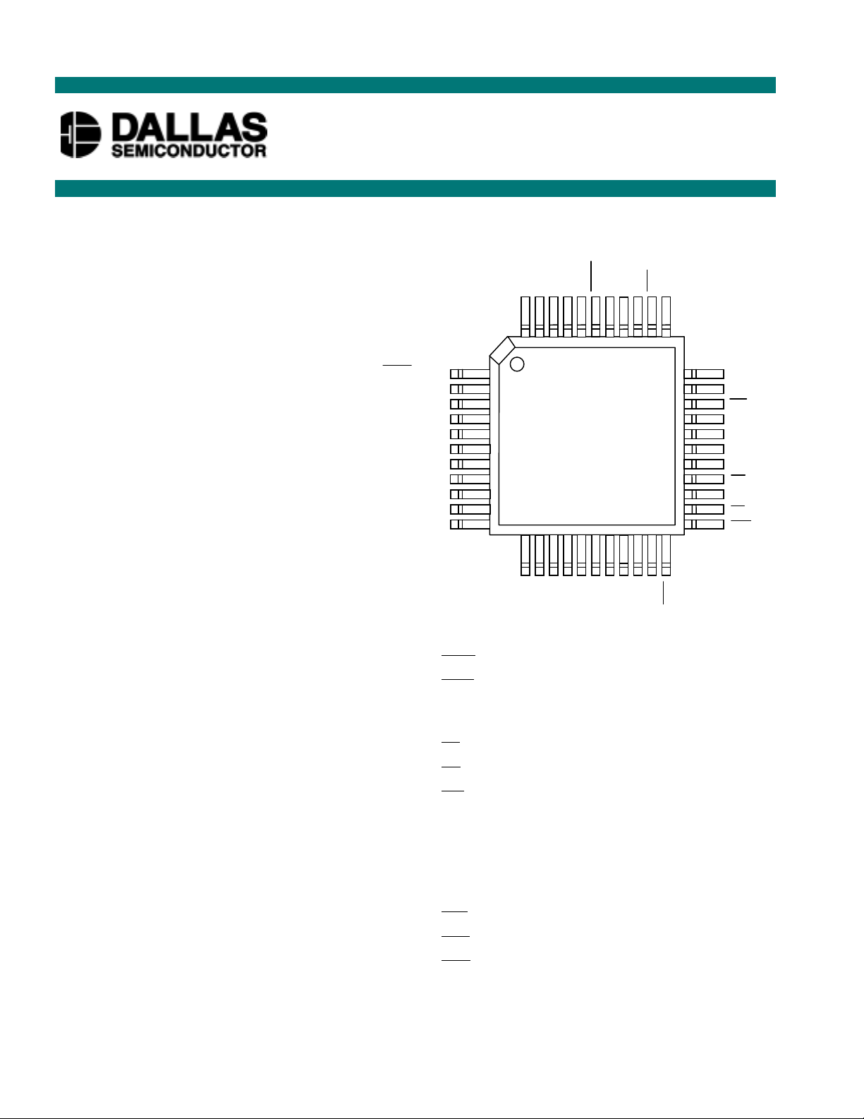
PIN ASSIGNMENT
A14
A12
A7
A6
A5
A4
A3
A2
A1
CCVCCO
INTA
V
X1X2GND
GND
44 34
C
11
12
A0
A16
2
3
4
GND
5
D
D
D
0
1
D
D
D
SQW
6
D
PF0
7
D
BAT2
V
22
CEO
33
23
PIN DESCRIPTION
INTA - Interrupt Output A (open drain)
INTB(INTB) - Interrupt Output B (open drain)
A0-A16 - Address Inputs
DQ0-DQ7 - Data Input/Output
CE - Chip Enable
A15
V
WE
A13
A8
A9
A11
OE
A10
CE
OE
BAT1
OE - Output Enable
WE - Write Enable
V
CC
- +5V Input
GND - Ground
NC - No Connection
SQW - Square Wave Output
X1, X2 - 32.768 kHz Crystal Connections
PFO - Power Fail Output
CEO - Chip Enable RAM
OER - Output Enable RAM
V
CCO
V
BAT1
V
BAT2
1 of 17 091300
- Voltage Out
- +3V Battery Input
- +3V Battery Input
Page 2

DS1384
DESCRIPTION
The DS1384 Watchdog Timekeeping Controller is a self-contained real time clock, alarm, watchdog
timer, and interval timer which provides control of up to 128k x 8 of external low power CMOS static
RAM in a 44-pin quad flat pack package. An external crystal and battery are the only components
required to maintain time of day and RAM memory contents in the absence of power. Access to all RTC
functions and the external RAM is the same as conventional bytewide SRAM. Data is maintained in the
Watchdog Timekeeper by intelligent control circuitry which detects the status of VCC and write protects
both memory and timekeeping functions when VCC is out of tolerance. Timekeeper information includes
hundredths of seconds, seconds, minutes, hours, day, date, month, and year. The date at the end of the
month is automatically adjusted for months with less than 31 days, including correction for leap year. The
timekeeper operates in either 12- or 24-hour format with an AM/PM indicator. The watchdog internal
timer provides watchdog alarm windows and interval timing between 0.01 seconds and 99.99 s econds.
The real time alarm provides for preset times of up to one week. All of the RTC functions and the
internal 50 bytes of RAM reside in the lower 64 bytes of the attached RAM memory map. The externally
attached static RAM is controlled by the DS1384 via the OER and CEO signals.
Automatic backup and write protection for an external SRAM is provided through the V
OER pins. The lithium energy source used to permanently power the real time clock is also used to retain
RAM data in the absence of VCC power through the V
pin. The chip enable output to RAM (CEO ) and
CCO
, CEO and
CCO
the output enable to RAM (OER ) are cont rolled during power transients to prevent data corruption. The
DS1384 is a complete one-chip solution in that an external crystal and battery ar e the only components
required to maintain time of day memory status in the absence of power.
SIGNAL DESCRIPTIONS
VCC, GND - DC power inputs: DC operating voltage is provided to the device on these pins. VCC is the
+5V input.
V
, V
BAT1
must be held between 2.4 and 4-volts for proper operation. In the absence of power, the DS1384 will have
a maximum load of 0.5 µA at 25°C. This should be added to the amount of current drawn from the
external RAM in standby mode at 25°C to size the external energy source. The DS1384 samples V
and V
BAT2
battery input must be grounded.
A16-A0 - Addr ess Bus (inputs): The address bus inputs qualified by CE , OE , WE , and VCC voltage are
used to select the on-chip 64 timekeeping/RAM registers within the memory map of the external SRAM
controlled as nonvolatile storage. When the qualified address bus value is within the range of
- Battery inputs for any standard 3-volt lithium cell or other energy source. Battery voltage
BAT2
BAT1
and always selects the battery with the higher voltage. If only one battery is used, the unused
00000H - 0003FH, one of the internal registers will be selected and
OER will remain inactive. When the
value is outside of the range, OE will be passed through to OER .
D7-D0 - Data Bus (bi-directional): When a qualified address from 00000H throu gh 0003FH is presented
to the device, data is passed to or from the on-chip 64 timekeeping/RAM registers via the data bus lines.
Data will be written on the rising edge of WE when CE is active. If CE is active without WE , data is
read from the device and driven onto the data bus pins when OE is low.
2 of 17
Page 3

DS1384
V
- Switched DC power for SRAM (output): This pin will be connected to V
CCO
above VSO (the greater of V
BAT1
or V
). When VCC voltage falls below this level, V
BAT2
when VCC voltage is
CC
will be
CCO
connected to the higher voltage battery pin.
CEO - RAM chip enable (output; active low): When power is good the CE input will be passed through
to CEO . If VCC is below VPF, CEO will remain at an inactive high level.
OER - RAM output enable (output; active low): When power is good and the address value is not within
the range of 00000H and 0003FH, and CE is active, the OE input will be passed through to OER . If these
conditions are not met, OER will remain at an inactive high level.
CE - Chip enable (input; active low): The chip enable signal must be asserted low during a bus cycle to
access the on-chip timekeeping RAM registers, or to access the external RAM via CEO .
OE - Output enable (input; active low): The output enable signal identifies the time period when either
the RTC or the external SRAM drives the bus with read data, provided that CE is valid with WE
disabled. When one of the 64 on-chip registers is selected during a re ad cycle, the OE is the enable signal
for the DS1384 output buffers and the data bus will be driven with read data. W hen the ex ternal RAM is
selected during a read cycle, the OE signal will be passed through to the OER pin so that read data will be
driven by the external SRAM.
WE - Write enable (input; active low): The write enable signal identifies the time period during which
data is written to either the on-chip registers or to an external SRAM location. When one of the on-chip
64 registers is addressed, data will be written to the selected register on the rising edge of WE .
INTA - Interrupt Output A (output; active low): Interrupt output A can be programmed as a Time of Day
Alarm or as a Watchdog Alarm (Interrupt output B becomes the alternate function). In addition, INTA
can be programmed to output either a pulse or a level.
INTB - Interrupt Output B (output; active high or low): Interrupt output B outputs the alarm (Time of
Day or Watchdog) that is not selected for
INTA . Interrupt output B is programmable high or low.
Both INTA and INTB(INTB) are open drain outputs. The two interrupts and the internal clock continue to
run regardless of the level of VCC. However, it is important to insure that the pull-up resistors used with
the interrupt pins are never pulled up to a value which is greater than V
+ 0.3V. As VCC falls below
CC
approximately 3.0 volts, a power switching circuit turns the lithium energy source on the maintain the
clock, and timer data functionality. It is also required to insure that during this time (battery backup
mode), the voltage present at INTA and INTB (INTB) does never exceed V
. At all times the current on
BAT
each should not exceed +2.1 mA or -1.0 mA.
X1, X2 - Cr ystal inputs: Connections for a standard 32.768 kHz quartz crystal. When ordering, request a
load capacitance or 6 pF. The internal oscillator circuitry is designed for operation with a crystal having a
specified load capacitance (CL) of 6 pF.
3 of 17
Page 4

DS1384
For more information on crystal selection and crystal layout considerations, please c onsult Application
Note 58, “Crystal Considerations with Dallas Real Time Clocks.”
SQW - Square Wave (output): This pin can be programmed to output a 1024 Hz square wave signal.
When the signal is turned off, the pin is high Z.
PFO - Power Fail Signal (output; active low when V
V
>4.5 volts.
CC
occurs): High state occurs t
WP
after power-up and
REC
ADDRESS DECODING
The DS1384 accommodates 17 address lines, which allows direct connection of up to 128k b ytes of static
RAM. The lower 14 bytes of RAM, regardless of the density used, will always contain the timekeeping,
alarm, and watchdog registers. The 14 clock registers reside in the lower 14 RAM locations without
conflict by inhibiting the OER (output enable RAM) signal during clock access. Since the watchdog
timekeeping chip actually contains 64 registers (14 RTC and 50 user RAM), the lower 64 bytes of any
attached memory resides within the DS1384. However, the RAM’s physical location is transparent to the
user and the memory map looks continuous from the first clock address to the upper most attached RAM
address.
OPERATION - READ CYCLE
The DS1384 executes a read cycle wh eneve r WE is inactive (high) and CE and OE are active (l ow). The
unique address specified by the address inputs (A0-A16) defines which of the on-chip 64 RTC/RAM or
external SRAM locations is to be accessed. When the address value pres ented to the DS1384 is in the
range of 00000H through 0003FH, one of the 64 on-chip registers will be selected and valid data will be
available to the eight data output drivers within t
providing that the CE and OE access times are also satisfied. If they are not, then data access must be
(access time) after the address input signal is stable,
ACC
measured from the latter occurri ng signal (CE or OE ) and the limiting parameter is either tCO for CE or
tOE for OE rather than the address access time. When one of the on-chip registers is selected for read, the
OER signal will remain inactive throughout the read cycle.
When the address value presented to the DS1384 is in the range of 00040H through 1FFFFH, an external
SRAM location will be selected. In this case the OE signal will be passed to the OER pin, with the
specified delay times of t
AOEL
or t
OERL
.
OPERATION - WRITE CYCLE
The DS1384 is in the write mode whenever the WE (Write Enable) and CE (Chip Enable) si gnals are in
the active (low) state after the address inputs are stable. The latter occurrin g falling edge of
will determine the start of the write cycle. The write cycle is terminated by the earlier rising edge of CE
or WE . All address inputs must be kept valid throughout the write cycle. WE must return to the high state
for a minimum recovery state (t
bus with sufficient Data Set Up (t
CE or WE . The OE control signal should be kept inactive (high) during write cycles to avoid bus
contention. However, if the output bus has been enabled (
outputs in t
from its falling edge.
WEZ
) before another cycle can be initiated. Data must be valid on the data
WR
) and Data Hold Time (tDH) with respect to the earlier rising edge of
DS
CE and OE active), then WE will disable the
CE or WE
4 of 17
Page 5

DS1384
When the address value presented to the DS1384 during the write is in the range of 00000H through
0003FH, one of the 64 on-chip registers will be selected and data will be written into the device.
When the address value presented to the DS1384 during the write is in the range of 00040H through
1FFFFH, an external SRAM location will be selected.
DATA RETENTION MODE
When V
with read or write cycles. However, wh en V
protection occurs) the internal clock registers and external RAM is blocked from access. This is
is within nominal limits (VCC > 4.5 volts) the DS1384 can be accessed as described above
CCI
is below the power-fail point, VPF, (point at which write
CC
accomplished internally by inhibiting access to the clock registers via the
power fail output signal (
External RAM access is inhibited in a similar manner by forcing
0.2 volts of the V
CCI
condition. When V
the V
pin to the V
CCI
External RAM is also powered by the V
V
pin is capable of supplying 100 µA of current to the attached m emory with less than 0.3 volts drop
CCO
under this condition. On power-up, when V
PFO) is driven active and will remain active until V
CEO to high level. This level is within
input. CEO will remain at this level as long as V
falls below the level of the battery (V
CCI
pin and the clock registers are maintained from the attached battery supply.
BAT
input when V
BAT
returns to in-tolerance conditions, write protection
CCI
CCI
or V
BAT1
BAT2
is below V
CE signal. At this time the
returns to nominal levels.
CC
remains at an out-of-tolerance
CCI
), power input is switched from
pin through the V
BAT
pin. The
CCO
continues for 150 ms by inhibiting CEO . The PFO signal also remains active during this time. The
DS1384 is capable of supporting two batteries which are used in a redundant fashion for applications
which require added reliability or increased battery capacity. When two batteries are used, the higher of
the two is selected for use. A selected battery will remain as backup supply until it is significantly below
the other. When the selected battery voltage falls below the alternate battery by about 0.6 volts, the
alternate battery is selected and then becomes the backup supply. This switching occurs transparently to
the user and continues until both batteries are exhausted. When only a single battery is required, both
battery inputs can be connected together. However, a more effective method of using a single battery
supply is to ground the unused battery input. When using a single battery, V
is the preferred input.
BAT1
WATCHDOG TIMEKEEPER REGISTERS
The DS1384 Watchdog Timekeeper Controller has 14 internal registers, which are 8 bits wide and
contain all of the Timekeeping, Alarm, Watchdog, Control, and Data information. The Clock, Calendar,
Alarm and Watchdog Registers are memory locations, which contain external (user accessible) and
internal copies of the data. The ex ternal copies are independent of interna l functions except that they are
updated periodically by the simultaneous transfer of the incremented internal copy (see Figure 1). The
Command Register bits are affected by both internal and external functions. This register will be
discussed later. The 50 bytes of RAM registers are accessed from t he external address and data bus and
reside or overlay external static RAM. Registers 0, 1, 2, 4, 6, 8, 9 and A contain time of da y and date
information (see Figure 2). Time of day information is stored in BCD. Registers 3, 5, and 7 contain the
time of day alarm information. Time of day alarm information is stored in BCD. Register B is the
Command Register and information in this register is binary. Register C and D ar e the Watchdog Alarm
Registers and information, which is stored in these two registers, is in BCD. Registers 0000EH through
register 0003FH are on-chip user bytes and can be used to contain data at the user’s discretion.
5 of 17
Page 6
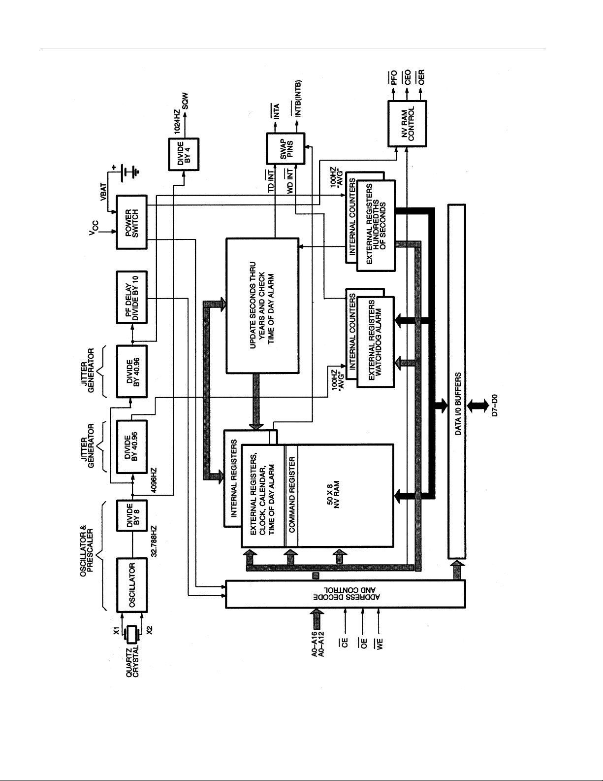
DS1384 BLOCK DIAGRAM Figure 1
DS1384
6 of 17
Page 7

DS1384 WATCHDOG TIMEKEEPER REGISTERS Figure 2
DS1384
7 of 17
Page 8

DS1384
TIME OF DAY ALARM MASK BITS Figure 3
REGISTER
MINUTES HOURS DAYS
1 1 1 ALARM ONCE PER MINUTE
0 1 1 ALARM WHEN MINUTES MATCH
0 0 1 ALARM WHEN HOURS AND MINUTES MATCH
0 0 0 ALARM WHEN HOURS, MINUTES, AND DAYS MATCH
NOTE:
ANY OTHER BIT COMBINATIONS OF MASK BIT SETTINGS PRODUCE ILLOGICAL
OPERATION.
TIME OF DAY REGISTERS
Registers 0, 1, 2, 4, 6, 8, 9 and A contain time of day data in BCD. Ten bits within these eight registers
are not used and will always read 0 regardless of how they are written. Bits 6 and 7 in the Months
Register (9) are binary bits.
When set to logical 0, EOSC (bit 7) enables the real-time clock oscillator. This bit will normally be turned
on by the user during device initialization. However, the oscillator can be turn ed on and o ff as necess ary
by setting this bit to the appropriate level.
Bit 6 of this same byte controls the square wave output (pin 24). When set to logical 0, the square wave
output pin will output a 1024 Hz square wave signal. When set to logic 1 the square wave output pin is in
a high impedance state.
Bit 6 of the Hours Register is defined as the 12- or 24-Hour Select Bit. When set to logic 1, th e 12-hour
format is selected. In the 12-hour format, bit 5 is the AM/ PM bit with logical one being PM. In the 24hour mode, bit 5 is the second 10-hour bit (20-23 hours). The time of day registers are updated every 0.01
seconds from the real time clock, except when the TE bit (bit 7 of register B) is set low or the clock
oscillator is not running.
The preferred method of synchronizing data access to and from the Watchdog Timekeeper is to access the
Command Register by doing a write cycle to address location 0B and setting the TE bit (Transfer Enable
bit) to a logic 0. This will freeze the external time of day registers at the present recorded time allowing
access to occur without danger of simultaneous update. When the watch registers have been read or
written a second write cycle to location 0B, setting the TE bit to a logic 1, will put the time of day
registers back to being updated every 0.01 second. No time is lost in the real time clock because the
internal copy of the time of day register buffers are continually incremented while the external memory
registers are frozen. An alternate method of reading and writing the time of day registers is to ignore
synchronization. However, any single read may give erroneous data as the real time clock may be in the
process of updating the external memory registers as data is being read.
The internal copies of seconds through years are incremented and Time of Da y Alarm is checked during
the period that hundredths of seconds reads 99 and are transferred to the external register when
hundredths of seconds roll from 99 to 00. A way of making sure data is valid is to do multiple reads and
compare. Writing the registers can also produce erroneous results for the same reasons. A way of making
sure that the write cycle has caused proper update is to do read verifies and re-execute the write c ycle if
data is not correct. While the possibility of erroneous results from reads and write cycles has been stated,
it is worth noting that the probability of an incorrect result is kept to a minimum due to the redundant
structure of the Watchdog Timekeeper.
8 of 17
Page 9

DS1384
TIME OF DAY ALARM REGISTERS
Registers 3, 5, and 7 contain the time of day alarm registers. Bits 3, 4, 5, and 6 of register 7 will always
read 0 regardless of how they are written. Bit 7 of registers 3, 5, and 7 are mask bits (Figure 3). When all
of the mask bits are logic 0, a time of day alarm will only occur when registers 2, 4, and 6 match the
values stored in registers 3, 5, and 7. An alarm will be generated every day when bit 7 of register 7 is set
to a logic 1. Similarly, an alarm is generated every hour when bit 7 of registers 7 and 5 is set to a lo gic 1.
When bit 7 of registers 7, 5, and 3 is set to a logic 1, an alarm will occur every minute when register 1
(seconds) rolls from 59 to 00.
Time of day alarm registers are written and read in the same format as the time of day registers. The time
of day alarm flag and interrupt is always cleared when alarm registers are read or written.
WATCHDOG ALARM REGISTERS
Registers C and D contain the time for the Watchdog Alarm. The two registers contain a time count f rom
00.01 to 99.99 seconds in BCD. The value written into the Watchdog Alarm Registers can be written or
read in any order. Any access to Register C or D will cause the Watchdog Alarm to reinitialize and clears
the Watchdog Flag Bit and the Watchdog Interrupt Output. When a new value is entered or the Watchdog
Registers are read, the Watchdog Timer will start counting down from the entered value to 0. When 0 is
reached, the Watchdog Interrupt Output will go to the active state. The Watchdog Timer Countdown is
interrupted and reinitialized back to the entered value every time either of the registers are accessed. In
this manner, controlled periodic accesses to the Watchdog Timer can prevent the Watchdog Alarm from
ever going to an active level. If access does not occur, countdown alarm will be repetitive. The
Watchdog Alarm Registers always read the entered value. The actual count down register is internal and
is not readable. Writing registers C and D to 0 will disable the Watchdog Alarm feature.
COMMAND REGISTER
Address location 0Bh is the Command Register where mask bits, control bits and flag bits reside. The
operation of each bit is as follows:
TE - Bit 7 Transfer enable - This bit when set to a logic 0 will disable the transfer of data between
internal and external clock registers. The contents in the external clo ck registers are now froz en and reads
or writes will not be affected with updates. This bit must be set to a logic 1 to allow updates.
IPSW - Bit 6 Interrupt switch - When set to a logic 1,
is the Watchdog Alarm. When set to logic 0, this bit reverses the output pins.
Alarm output and INTB/(INTB) is the Time of Day Alarm output.
IBH/LO - Bit 5 Interrupt B Sink or Source Current -When this bit is set to a logic 1 and VCC is applied,
INTB/(INTB) will source current (see DC characteristics I
sink current (see DC characteristics IOL).
PU/LVL - Bit 4 Interrupt pulse mode or level mode - This bit determines whether both interrupts will
output a pulse or level signal. When set to a logic 0, INTA and INTB/(INTB) will be in the level mode.
When this bit is set to a logic 1, the pulse mode is selected and INTA will sink current for a minimum of
3 ms and then release. INTB /(INTB) will either sink or source current, depending on the condition of bit
5, for a minimum of 3 ms and then release.
INTA is the Time of Day Alarm and INTB /(INTB)
INTA is now the W atchdog
). When this bit is set to a logic 0, INTB will
OH
9 of 17
Page 10

DS1384
WAM - Bit 3 Watchdog Alarm Mask - When this bit is set to a logic 0, the Watchdog Interrupt output
will be activated. The activated state is determined by bits 1,4,5, and 6 of the Command Register. When
this bit is set to a logic 1, the Watchdog interrupt output is deactivated.
TDM - Bit 2 Time of Day Alarm Mask - When this bit is set to a logic 0, the Time of Day Alarm
Interrupt output will be activated. The activated state is determined by bits 0, 4, 5, and 6 of the Command
Register. When this bit is set to a logic 1, the Time of Day Alarm interrupt output is deactivated.
WAF - Bit 1 Watchdog Alarm Flag - This bit is set to a logic 1 when a watchdog alarm interrupt occurs.
This bit is read-only.
The bit is reset when any of the Watchdog Alarm registers are accessed.
When the interrupt is in the pulse mode (see bit 4 definition), this flag will be in the logic 1 state only
during the time the interrupt is active.
TDF - Bit 0 Time of Day Flag - This is a read-only bit. This bit is set to a logic 1 when a time of day
alarm has occurred. The time the alarm occurred can be determined by reading the Time of Day Alarm
registers. This bit is reset to a logic 0 state when any of the Time of Day Alarm registers is accessed.
When the interrupt is in the pulse mode (see bit 4 definition), this flag will be in the logic 1 state only
during the time the interrupt is active.
10 of 17
Page 11

DS1384
ABSOLUTE MAXIMUM RATINGS*
Voltage on Any Pin Relative to Ground -0.3V to +7.0V
Operating Temperature 0°C to 70°C
Storage Temperature -20°C to +70°C
Soldering Temperature See J-STD-020A Specification
✻
This is a stress rating only and functional operation of the devic e at these or any other conditions above
those indicated in the operation sections of this specification is not implied. Exposure to absolute
maximum rating conditions for extended periods of time may affect reliability.
RECOMMENDED DC OPERATING CONDITIONS (0°C to 70°C)
PARAMETER SYMBOL MIN TYP MAX UNITS NOTES
Supply Voltage V
Logic 1 Voltage All Inputs V
Logic 0 Voltage All Inputs V
Battery Input Voltage V
CC
IH
IL
BAT
4.5 5.5 V 1
2.0 VCC+0.3 V
-0.3 0.8 V
2.4 4.0V V
DC ELECTRICAL CHARACTERISTICS (0°C to 70°C; VCC = 5V ± 10%)
PARAMETER SYMBOL MIN TYP MAX UNITS NOTES
Average VCC Power
Supply Current
TTL Standby Current
(CE = VIH)
CMOS Standby Current
(CE VCC-0.2V)
Input Leakage Current
(any input)
Output Leakage Current I
Output Logic 1 Voltage
(IOH = -1.0 mA)
Output Logic 0 Voltage
(IOH = +2.1 mA)
Output Voltage V
Output Current I
Write Protection Voltage V
Output Voltage V
Output Current I
Battery Leakage OSC ON I
Battery Leakage OSC OFF I
Switch Over Voltage V
I
CC1
I
CC2
I
CC3
I
IL
IO
V
OH
V
OL
CCO1
CCO1
PF
CCO2
CCO2
BAT1
BAT2
SO
7 15 mA 2, 3
2 5 mA 2, 3
1 3 mA 2, 3
1+1µA
-1 +1 µA
2.4 V
0.4 V
VCC-
V4
0.3
85 mA 4
4.0 4.25 4.5 V 5
V
BAT
V6
-0.3
100 µA 6
500 nA
100 nA
V
V
BAT1
BAT2
,
V
11 of 17
Page 12

DS1384
AC ELEC TRICAL CHARACTERI STICS (0°C to 70°C; VCC = 5.0V ±10%)
PARAMETER SYMBOL MIN TYP MAX UNITS NOTES
Read Cycle Time t
Address Access Time t
CE Access Time
CE Data Off Time
Output Enable Access
Time
Output Enable Data
Off Time
Output Enable to DQ
Low-Z
CE to DQ Low-Z
Output Hold from Address t
CE to CEO Low or High
OE Low to OER Low
t
t
A0-A16 > 00040h
OE High to OER High
Time
Address 00040h-1FFFFh
t
to OER Low
Address 00000h-0003Fh to
OER High
t
Write Cycle Time t
Address Setup Time t
CE Pulse Width
Address Hold from
End of Write
Write Pulse Width t
CE Data Off Time
WE Data Off Time
WE or CE Inactive Time
Data Setup Time t
Data Hold Time High t
INTA and INTB Pulse
Width
RC
ACC
t
CO
t
CEZ
t
OE
t
OEZ
t
OEL
t
CEL
OH
CEPD
OERL
t
RO
AOEL
AOEH
WC
AW
t
CEW
t
AH
WP
t
CEZ
t
WEZ
t
WR
DS
DH
t
IPW
120 ns
120 ns
120 ns
40 ns
60 ns
40 ns
5ns
10 ns
5ns
25 ns
20 ns
20 ns
50 ns
40 ns
120 ns
0ns
120 ns
10 ns
80 ns
40 ns
40 ns
10 ns
45 ns
0ns
3ms
AC TEST CONDITIONS
Input Levels: 0V to 3V
Transition Times: 5 ns
12 of 17
Page 13

DS1384
CAPACITANCE (tA = 25°C)
PARAMETER SYMBOL MIN TYP MAX UNITS NOTES
Capacitance on all pins
C
I
715pF
(except DQ)
Capacitance on DQ pins C
DQ
715pF
AC ELEC TRICAL CHARACTERI STICS (0°C to 70°C)
PARAMETER SYMBOL MIN TYP MAX UNITS NOTES
CE at V
before Power
IH
Down
VPF (Max) to VPF (Min)
VCC Fall Time
VPF (Min) to VSO VCC Fall
Time
VPF (Min) to VPF (Max)
VCC Rise Time
Power Up t
Expected Data Retention
Time (Oscillator On)
t
PD
t
F
t
FB
t
R
REC
t
DR
0µs
300 µs
10 µs
0µs
10 150 ms
10 years 7
READ CYCLE TIMING: RTC AND EXTERNAL SRAM CONTROL SIGNALS
13 of 17
Page 14

OER TIMING WHEN SWITCHING BETWEEN LOWER MEMORY (00000h-
0003Fh) AND UPPER MEMORY (00040h-1FFFFh)
WRITE CYCLE TIMING: RTC AND EXTERNAL SRAM CONTROL SIGNALS
DS1384
14 of 17
Page 15

TIMING DIAGRAM: POWER UP
DS1384
TIMING DIAGRAM: POWER DOWN
15 of 17
Page 16

DS1384
TIMING DIAGRAM: INTERRUPT OUTPUTS PULSE MODE (SEE NOTES 8, 9)
NOTES:
1. All voltages are referenced to ground.
2. Typical values are at 25°C and nominal supplies.
3. Outputs are open.
4. Value for voltage and currents is from the V
5. Write protection trip point occurs during power fail prior to switchover from VCC to V
6. Value for voltage and currents is from the V
input pin to the V
CCI
input pin to the V
BAT
CCO
CCO
pin.
pin.
BAT
.
7. Data retention time depends on the size of battery selected and the amount of current demanded by
the static RAM in back-up mode. The batter y capaci t y (mA •=hr) to achiev e a T
by the formula: C=(I
BAT1
+ I
) x 24 x 365 x 10, where I
RAM
is the standby current of the static
RAM
of 10 years is given
DR
RAM at the battery voltage. For the DS1384 chip alone, a standard 48 mAh lithium cell battery will
provide greater than 10 years of data retention in the absence of power.
8. Applies to both interrupt pins when the alarms are set to pulse.
9. Interrupt output occurs within 100 ns of the alarm condition existing.
OUTPUT LOAD
16 of 17
Page 17

DS1384 FP PACKAGE OUTLINES
DS1384
NOTES:
1. DIMENSIONS D1 AND E1 INCLUDE
MOLD MISMATCH, BUT DO NOT
INCLUDE MOLD PROTRUSION;
ALLOWABLE PROTRUSION IS 0.25 MM
PER SIDE.
2. DETAILS OF PIN 1 IDENTIFIER ARE
OPTIONAL BUT MUST BE LOCATED
WITHIN THE ZONE INDICATED.
3. ALLOWABLE DAMPER PROTRUSION
IS 0.08 MM TOTAL IN EXCESS OF THE
B DIMENSION; AT MAXIMUM
MATERIAL CONDITION. PROTRUSION
NOT TO BE LOCATED ON LOWER
RADIUS OF FOOT OF LEAD.
PKG DS1384FP
DIM MIN MAX
A - 2.45
A1 0.10 0.30
A2 1.95 2.10
D 13.65 14.30
D1 9.90 10.00
E 13.65 14.30
E1 9.90 10.00
L 0.63 1.03
e 0.80 BSC
B 0.30 0.45
C 0.13 0.23
56-G3001-001, 56-G4012-001
4. CONTROLLING DIMENSIONS:
MILLIMETERS.
17 of 17
 Loading...