

Page 1
General Description
The DS1375 digital real-time clock (RTC) is a low-power
clock/calendar that does not require a crystal. The
device operates from a digital clock input pin at one of
four frequencies: 32.768kHz, 8.192kHz, 60Hz, or 50Hz.
It maintains seconds, minutes, hours, day, date, month,
and year information. The date at the end of the month
is automatically adjusted for months with fewer than 31
days, including corrections for leap year. The clock
operates in either the 24-hour or 12-hour format with an
AM/PM indicator. Two programmable time-of-day/date
alarms, a programmable square-wave output, and 16
bytes of SRAM are provided. Address and data are
transferred serially through a 2-wire bidirectional bus.
Applications
RTC Complement to the DS32kHz TCXO
Utility Meters
Appliances
Consumer Electronics
Automotive
Features
♦ RTC Counts Seconds, Minutes, Hours, Day, Date,
Month, and Year with Leap-Year Compensation
Valid Up to 2100
♦ Two Programmable Alarms
♦ Programmable Square-Wave Output
♦ Operates from a 32.768kHz, 8.192kHz, 60Hz, or
50Hz Digital Clock Signal
♦ 16 Bytes of SRAM
♦ Fast (400kHz) 2-Wire Interface
♦ 1.7V to 5.5V Operation
DS1375
2-Wire Digital Input RTC with Alarm
______________________________________________ Maxim Integrated Products 1
Pin Configuration
Ordering Information
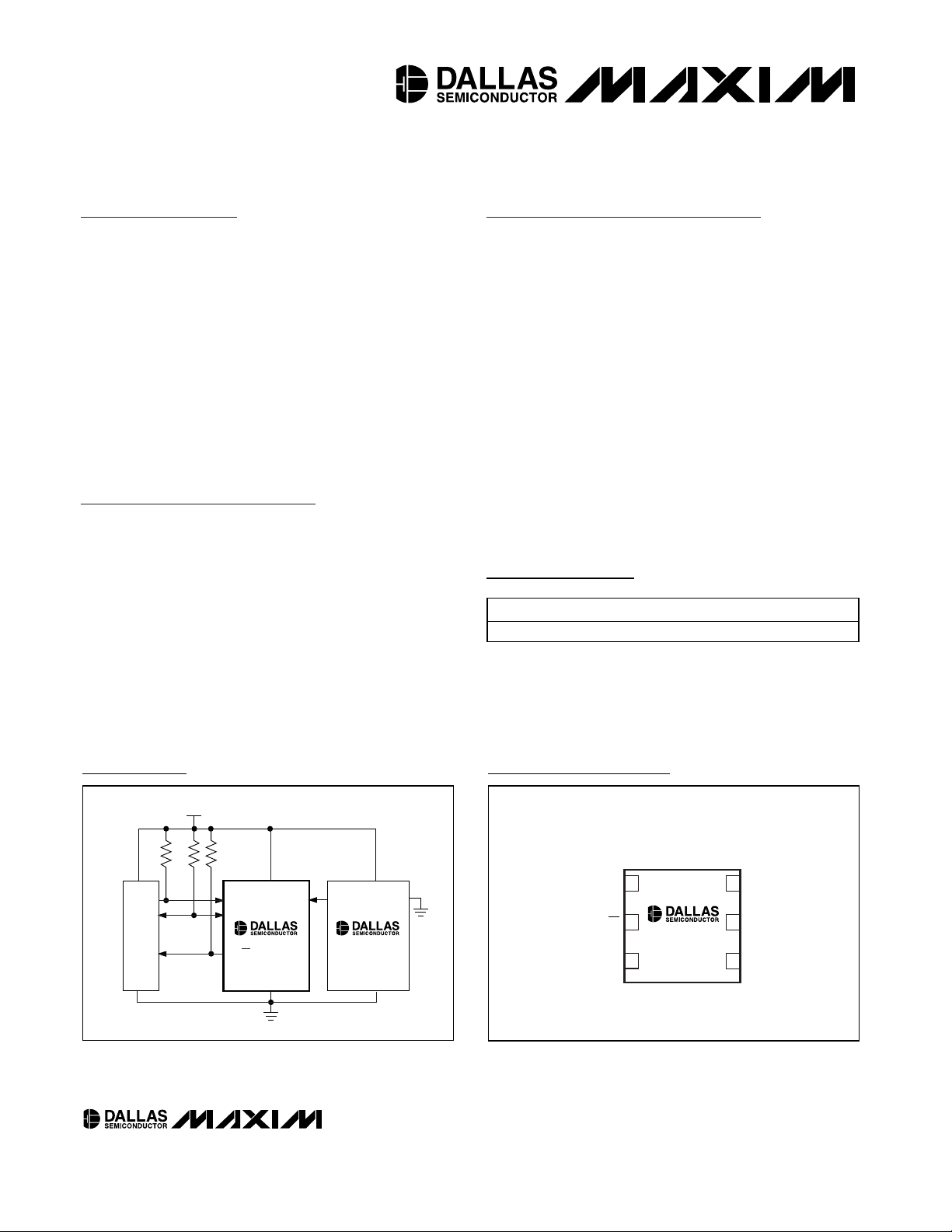
DS1375
V
CC
SCL CLK
SCA
GND
CPU
+3V
RPU RPU
RPU = t
r/CB
INT
DS32kHz
V
BAT
V
CC
GND
SQWINT
Typical Operating Circuit
Rev 0; 4/03
For pricing, delivery, and ordering information, please contact Maxim/Dallas Direct! at
1-888-629-4642, or visit Maxim’s website at www.maxim-ic.com.
PART TEMP RANGE PIN-PACKAGE TOP MARK
DS1375 -40°C to +85°C 6 Thin QFN DS1375
TOP VIEW
CLK
SQW/INT
16V
2
DS1375
34
THIN QFN
CC
5 SCL
SDAGND
Page 2
DS1375
2-Wire Digital Input RTC with Alarm
2 _____________________________________________________________________
ABSOLUTE MAXIMUM RATINGS
RECOMMENDED DC OPERATING CONDITIONS
(VCC= +1.7V to +5.5V, TA= -40°C to +85°C, unless otherwise noted. Typical values are at VCC= 3.3V, TA= +25°C, unless otherwise noted.) (Note 1)
Stresses beyond those listed under “Absolute Maximum Ratings” may cause permanent damage to the device. These are stress ratings only, and functional
operation of the device at these or any other conditions beyond those indicated in the operational sections of the specifications is not implied. Exposure to
absolute maximum rating conditions for extended periods may affect device reliability.
Note 1: Limits at -40°C are guaranteed by design and not production tested.
Note 2: All voltages are referenced to ground.
Note 3: For the CLK pin, input voltages above V
CC
+ 0.3V cause current to flow into the device. The input current must not
exceed the current drawn by the circuit that is connected to V
CC
. Otherwise, current flows out of the DS1375, raising the
voltage level on the VCCbus.
Note 4: V
IL MIN
on the CLK pin can exceed -0.3V as long as the current is limited to less than 1mA.
Note 5: I
CCA
—SCL clocking at max frequency = 400kHz.
Note 6: CLK pin running at 32,768Hz, rise and fall times at 10ns or less.
Note 7: Specified with 2-wire bus inactive.
Voltage Range on V
CC
Pin
Relative to Ground.............................................-0.3V to +6.0V
Voltage Range on SDA, SCL, and WDS
Relative to Ground....................................-0.3V to V
CC
+ 0.3V
Operating Temperature Range ...........................-40°C to +85°C
Storage Temperature Range .............................-55°C to +125°C
Soldering Temperature .......................................See IPC/JEDEC
J-STD-020A Specification
Supply Voltage V
Timekeeping Voltage V
Input Logic 1 (SDA, SCL) V
Supply Voltage, Pullup
(SQW/INT, CLK)
Input Logic 0 V
Input Leakage (SCL, CLK) I
I/O Leakage (SDA, SQW/INT)I
SDA Logic 0 Output I
SQW/INT Logic 0 Output I
Active Supply Current I
Standby Current I
PARAMETER SYMBOL CONDITIONS MIN TYP MAX UNITS
CC
V
PULLUP
LO
OLSDA
OLSQW
CCA
CCS
(Note 2) 1.7 3.3 5.5 V
(Note 2) 1.3 5.5 V
TK
(Note 2) 0.7 x V
IH
(Notes 2, 3) 5.5 V
(Notes 2, 4) -0.3
IL
LI
VCC > 2V; VOL = 0.4V
VCC < 2V; VOL = 0.2 x V
VCC > 2V; VOL = 0.4V
1.7V < VCC < 2V; VOL = 0.2 x V
1.3V < VCC < 1.7V; VOL = 0.2 x V
(Notes 5, 6) 33 150 µA
(Notes 6, 7) 150 500 nA
CC
CC
CC
CC
-1 +1 µA
-1 +1 µA
V
+ 0.3 V
CC
+0.3
V
CC
3.0 mA
3.0 mA
250 µA
V
Page 3
DS1375
2-Wire Digital Input RTC with Alarm
_____________________________________________________________________ 3
Note 8: After this period, the first clock pulse is generated.
Note 9: A device must internally provide a hold time of at least 300ns for the SDA signal (see the V
IHMIN
of the SCL signal) to
bridge the undefined region of the falling edge of SCL.
Note 10: The maximum t
HD:DAT
is only met if the device does not stretch the low period (t
LOW
) of the SCL signal.
Note 11: A fast-mode device can be used in a standard-mode system, but the requirement t
SU:DAT
≥ 250ns must then be met.
This is automatically the case if the device does not stretch the low period of the SCL signal. If such a device does
stretch the LOW period of the SCL signal, it must output the next data bit to the SDA line t
R MAX
+ t
SU:DAT
= 1000 + 250
= 1250ns before the SCL line is released.
Note 12: C
B
—total capacitance of one bus line in pF.
AC ELECTRICAL CHARACTERISTICS
(VCC= V
CCMIN
to V
CCMAX
, TA= -40°C to +85°C, unless otherwise noted.) (Note 1, Figure 1)
SCL Clock Frequency f
Bus Free Time Between STOP
and START Conditions
Hold Time (Repeated) START
Condition (Note 8)
Low Period of SCL Clock t
High Period of SCL Clock t
Data Hold Time (Notes 9, 10) t
Data Setup Time (Note 11) t
Start Setup Time t
Rise Time of Both SDA and SCL
Signals (Note 12)
Fall Time of Both SDA and SCL
Signals (Note 12)
Setup Time for STOP Condition t
Capacitive Load for Each Bus
Line (Note 12)
Pulse Width of Spikes that Must
be Suppressed by the Input Filter
PARAMETER SYMBOL CONDITIONS MIN TYP MAX UNITS
SCL
t
BUF
t
HD:STA
LOW
HIGH
HD:DAT
SU:DAT
SU:STA
t
t
SU:STO
C
t
SP
Fast mode 100 400
Standard mode 0 100
Fast mode 1.3
Standard mode 4.7
Fast mode 0.6
Standard mode 4.0
Fast mode 1.3
Standard mode 4.7
Fast mode 0.6
Standard mode 4.0
Fast mode 0 0.9
Standard mode 0 0.9
Fast mode 100
Standard mode 250
Fast mode 0.6
Standard mode 4.7
Fast mode 300
R
Standard mode
Fast mode 300
F
Standard mode
Fast mode 0.6
Standard mode 4.7
B
Fast mode 30 ns
20 + 0.1C
20 + 0.1C
kHz
µs
µs
µs
µs
µs
ns
µs
B
B
1000
300
400 pF
ns
ns
µs
Page 4
I
CCS
vs. V
CC
DS1375 toc01
VCC (V)
SUPPlY CURRENT (nA)
5.24.74.23.73.22.72.2
100
150
200
250
300
50
1.7
I
CCA
vs. V
CC
SUPPLY CURRENT (µA)
10
20
30
40
50
60
70
80
90
100
0
DS1375 toc02
VCC (V)
5.24.74.23.73.22.72.21.7
Typical Operating Characteristics
(VCC= +3.3V, TA= +25°C, unless otherwise noted.)
DS1375
2-Wire Digital Input RTC with Alarm
4 _____________________________________________________________________
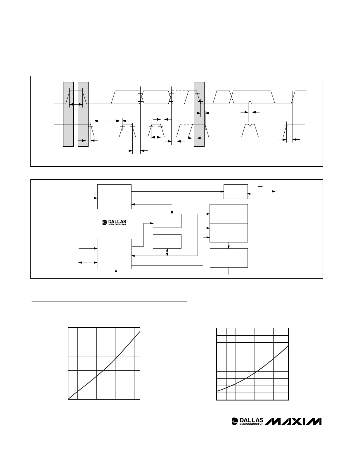
Figure 1. Data Transfer on 2-Wire Serial Bus
Figure 2. Functional Diagram
SDA
t
BUF
t
LOW
SCL
STOP START
t
HD:STA
CLK
SCL
SDA
DIVIDER
DS1375
SERIAL BUS
INTERFACE AND
ADDRESS
REGISTER
t
R
t
HD:DAT
t
F
t
HIGH
t
SU:DAT
8192Hz/4096Hz/1024Hz/1Hz
1Hz
CONTROL
LOGIC
SRAM
REPEATED
START
t
SU:STA
t
HD:STA
ALARM AND
REGISTERS
CLOCK AND
CALENDAR
REGISTERS
USER BUFFER
CONTROL
(7 BYTES)
MUX/
BUFFER
SQW/INT
t
SP
t
SU:STO
Page 5

DS1375
2-Wire Digital Input RTC with Alarm
_____________________________________________________________________ 5
Typical Operating Characteristics (continued)
(VCC= +3.3V, TA= +25°C, unless otherwise noted.)
Pin Description
Detailed Description
The DS1375 digital input RTC with alarm is a low-power
clock/calendar with two programmable time-of-day
alarms and a programmable square-wave output.
Address and data are transferred serially through the
2-wire serial interface bus. The clock/calendar provides
seconds, minutes, hours, day, date, month, and year
information. The date at the end of the month is automatically adjusted for months with fewer than 31 days,
including corrections for leap year. The clock operates
in either the 24-hour or 12-hour format with an AM/PM
indicator. The DS1375 requires an external clock
source selectable between 32,768Hz, 8192Hz, 60Hz,
or 50Hz for the timekeeping function. Sixteen bytes of
SRAM are provided for additional user storage.
Operation
The DS1375 operates as a slave device on the serial
bus. Access is obtained by implementing a START
condition and providing a device identification code,
followed by data. Subsequent registers can be
accessed sequentially until a STOP condition is executed. The functional diagram in Figure 2 shows the main
elements of the serial RTC.
Address Map
Table 1 shows the address map for the timekeeping
registers and SRAM. The 16 bytes of SRAM occupy
addresses 10–1Fhex. During a multibyte access, when
the address pointer reaches the end of the register
space (1Fh), it wraps around to location 00h. On a
2-wire START, STOP, or address pointer incrementing
I
I
135.0
132.5
130.0
127.5
125.0
122.5
SUPPLY CURRENT (nA)
120.0
117.5
115.0
CCS
-40
vs. TEMPERATURE
VCC = 3.0V
TEMPERATURE (°C)
500
DS1375 toc03
8060-20 0 20 40
450
400
350
300
250
200
150
SUPPLY CURRENT (µA)
100
50
0
0 5.0
vs. CLK INPUT VOLTAGE
CCS
VCC = 5.0V
CLK VOLTAGE (V)
PIN NAME FUNCTION
1 CLK
2 SQW/INT Square-Wave/Interrupt Output. This pin is open drain and requires an external pullup resistor.
3 GND Ground
4 SDA
5 SCL
6VCCDC Power for Primary Power Supply
Digital Clock Input. This pin must be 32,768Hz, 8192Hz, 60Hz, or 50Hz square wave, 45% to 55%
duty cycle.
Serial Data Input/Output. SDA is the data input/output for the 2-wire serial interface. It is open drain
and requires an external pullup resistor.
Serial Clock Input. SCL is the clock input for the 2-wire serial interface, and is used to synchronize
data movement on the serial interface.
DS1375 toc04
VCC = 4.0V
4.54.03.0 3.51.0 1.5 2.0 2.50.5
Page 6

to location 00h, the current time is transferred to a second set of registers. The time information is read from
these secondary registers, while the clock may continue to run. This eliminates the need to reread the registers in case the main registers update during a read.
Note: Unless otherwise specified, the state of the registers is not defined when power is first applied.
Clock and Calendar
The time and calendar information is obtained by reading the appropriate register bytes. Table 1 shows the
RTC registers. The time and calendar data are set or
initialized by writing the appropriate register bytes. The
contents of the time and calendar registers are in the
binary-coded decimal (BCD) format. The DS1375 can
be run in either 12-hour or 24-hour mode. Bit 6 of the
hours register is defined as the 12- or 24-hour mode
select bit. When high, the 12-hour mode is selected. In
the 12-hour mode, bit 5 is the AM/PM bit with logic high
being PM. In the 24-hour mode, bit 5 is the second 10hour bit (20–23 hours). The century bit (bit 7 of the
month register) is toggled when the years register overflows from 99 to 00.
The day-of-week register increments at midnight.
Values that correspond to the day of week are userdefined but must be sequential (i.e., if 1 equals
Sunday, then 2 equals Monday, and so on). Illogical
time and date entries result in undefined operation.
When reading or writing the time and date registers,
secondary (user) buffers are used to prevent errors
when the internal registers update. When reading the
time and date registers, the user buffers are synchronized to the internal registers on any START or STOP
and when the register pointer rolls over to zero. The
time information is read from these secondary registers,
while the clock continues to run. This eliminates the
need to reread the registers in case the main registers
update during a read.
DS1375
2-Wire Digital Input RTC with Alarm
6 _____________________________________________________________________
Table 1. Timekeeping Registers and SRAM
ADDRESS BIT 7 BIT 6 BIT 5 BIT 4 BIT 3 BIT 2 BIT 1 BIT 0 FUNCTION RANGE
00h 0 10 Seconds Seconds Seconds 00–59
01h 0 10 Minutes Minutes Minutes 00–59
02h 0 12/24
03h 0 0 0 0 0 Day Day 1–7
04h 0 0 10 Date Date Date 00–31
05h Century 0 0
06h 10 Year Year Year 00–99
07h A1M1 10 Seconds Seconds Alarm 1 Seconds 00–59
08h A1M2 10 Minutes Minutes Alarm 1 Minutes 00–59
09h A1M3 12/24
0Ah A1M4 DY/DT
0Bh A2M2 10 Minutes Minutes Alarm 2 Minutes 00–59
0Ch A2M3 12/24
0Dh A2M4 DY/DT
0Eh ECLK CLKSEL1 CLKSEL0 RS2 RS1 INTCN A2IE A1IE Control —
0Fh 0 0 0 0 0 0 A2F A1F
10h–1Fh B7 B6 B5 B4 B3 B2 B1 B0 SRAM 00–FFH
AM/PM
10 Hours
AM/PM
10 Hours
AM/PM
10 Hours
10 Hours Hours Hours
10
Month
10 Hours Hours Alarm 1 Hours
10 Date Date Alarm 1 Date 1–31
10 Hours Hours Alarm 2 Hours
— Day Alarm 2 Day 1–7
10 Date Date Alarm 2 Date 1–31
Months
Day Alarm 1 Day 1–7
Month/
Century
Control/
Status
1–12 + AM/PM
00–23
01–12 +
Century
1–12 + AM/PM
00–23
1–12 + AM/PM
00–23
—
Page 7

DS1375
2-Wire Digital Input RTC with Alarm
_____________________________________________________________________ 7
Table 2. Alarm Mask Bits
ALARM 1 REGISTER MASK
BITS (BIT 7)
ALARM RATE
X 1111
Alarm once per
second
X 1110
Alarm when seconds
match
X 1100
Alarm when minutes
and seconds match
X 1000
Alarm when hours,
minutes, and seconds
match
0 0000
Alarm when date,
hours, minutes, and
seconds match
1 0000
Alarm when day,
hours, minutes, and
seconds match
ALARM 2 REGISTER
ALARM RATE
X 111
Alarm once per minute
(00 seconds of every min)
X 110Alarm when minutes match
X 100
Alarm when hours and
minutes match
0 000
Alarm when date, hours, and
minutes match
1 000
Alarm when day, hours, and
minutes match
The countdown chain is reset whenever the seconds
register is written. Write transfers occur on the acknowledge from the DS1375. Once the countdown chain is
reset, to avoid rollover issues the remaining time and
date registers must be written within 1 second. The 1Hz
square-wave output, if enabled, transitions high 500ms
after the seconds data transfer, provided the clock
input is already being driven.
Alarms
The DS1375 contains two time-of-day/date alarms.
Alarm 1 can be set by writing to registers 07h–0Ah.
Alarm 2 can be set by writing to registers 0Bh–0Dh.
The alarms can be programmed (by the alarm enable
and INTCN bits of the control register) to activate the
SQW/INT output on an alarm match condition. Bit 7 of
the time-of-day/date alarm registers are mask bits
(Table 2). When all the mask bits for each alarm are
logic 0, an alarm only occurs when the values in the
timekeeping registers match the corresponding values
stored in the time-of-day/date alarm registers. The
alarms can also be programmed to repeat every second, minute, hour, day, or date. Table 2 shows the possible settings. Configurations not listed in the table
result in illogical operation.
The DY/DT bits (bit 6 of the alarm day/date registers)
control whether the alarm value stored in bits 0–5 of
that register reflects the day of the week or the date of
the month. If DY/DT is written to logic 0, the alarm is the
result of a match with date of the month. If DY/DT is
written to logic 1, the alarm is the result of a match with
day of the week.
When the RTC register values match alarm register settings, the corresponding alarm flag A1F or A2F bit is
set to logic 1. If the corresponding alarm interrupt
enable A1IE or A2IE is also set to logic 1, and the
INTCN bit is set to logic 1, the alarm condition activates
the SQW/INT signal. The match is tested on the onceper-second update of the time and date registers.
Special Purpose Registers
The DS1375 has two additional registers (control and
status) that control the RTC, alarms, and square-wave
output.
DY/DT
A1M4 A1M3 A1M2 A1M1
DY/DT
MASK BITS (BIT 7)
A2M4 A2M3 A2M2
Page 8

Control Register (0Eh)
Bit 7/Enable Clock (ECLK). When ECLK is set to logic
1, the CLK input pin is enabled to clock the internal
divider chain and advance the timekeeping registers.
When ECLK is set to logic 0, the divider chain is held in
reset, and the time is not allowed to advance. To synchronize the DS1375 time to a reference, write the
ECLK bit to 0, write the time value, then write ECLK
back to 1. Doing so synchronizes the time value to within one period of the CLK pin from the point in the interface protocol where the ECLK bit is written. ECLK is set
to logic 1 when power is first applied.
Bits 6, 5/Clock Select Bits 1, 0 (CLKSEL1,
CLKSEL0). These bits determine how the CLK input
pin is divided down to get the 1Hz reference clock for
the timekeeping registers (Table 3). The CLKSEL0–1
bits are cleared to logic 0 when power is first applied.
Bits 4, 3/Rate Select (RS2 and RS1). These bits control the frequency of the square-wave output when the
square wave has been enabled and the CLKSEL0 and
CLKSEL1 bits are set to 0. Table 3 shows the squarewave frequencies that can be selected with the RS bits.
These bits are set to logic 1 (8.192kHz) when power is
first applied. If either CLKSEL0 or CLKSEL1 are logic 1,
the 1Hz signal is output.
Bit 2/Interrupt Control (INTCN). This bit controls the
SQW/INT signal. When the INTCN bit is set to logic 0, a
square wave is output on the SQW/INT pin. When the
INTCN bit is set to logic 1, a match between the timekeeping registers and either of the alarm registers activates the SQW/INT (if the alarm is also enabled). The
corresponding alarm flag is always set, regardless of
the state of the INTCN bit. The INTCN bit is set to logic
0 when power is first applied.
Bit 1/Alarm 2 Interrupt Enable (A2IE). When set to
logic 1, this bit permits the alarm 2 flag (A2F) bit in the
status register to assert SQW/INT (when INTCN = 1).
When the A2IE bit is set to logic 0 or INTCN is set to
logic 0, the A2F bit does not initiate an interrupt signal.
The A2IE bit is disabled (logic 0) when power is first
applied.
Bit 0/Alarm 1 Interrupt Enable (A1IE). When set to
logic 1, this bit permits the alarm 1 flag (A1F) bit in the
status register to assert SQW/INT (when INTCN = 1).
When the A1IE bit is set to logic 0 or INTCN is set to
logic 0, the A1F bit does not initiate the SQW/INT signal. The A1IE bit is disabled (logic 0) when power is
first applied.
DS1375
2-Wire Digital Input RTC with Alarm
8 _____________________________________________________________________
Table 3. CLK Input Frequency, Square-Wave Output Frequency
Bit 7 Bit 6 Bit 5 Bit 4 Bit 3 Bit 2 Bit 1 Bit 0
ECLK CLKSEL1 CLKSEL0 RS2 RS1 INTCN A2IE A1IE
INTCN CLKSEL1 CLKSEL0 INPUT FREQUENCY RS2 RS1
1X X As selected X X N/A (Interrupt)
00 0 32,768Hz 0 0 1Hz
00 0 32,768Hz 0 1 1.024kHz
00 0 32,768Hz 1 0 4.096kHz
00 0 32,768Hz 1 1 8.192kHz
00 1 8192Hz X X 1Hz
01 0 60Hz X X 1Hz
01 1 50Hz X X 1Hz
SQUARE-WAVE OUTPUT
FREQUENCY
Page 9

Status Register (0Fh)
Bit 1/Alarm 2 Flag (A2F). A logic 1 in the alarm 2 flag
bit indicates that the time matched the alarm 2 registers. If the A2IE bit is logic 1 and the INTCN bit is set to
logic 1, the SQW/INT pin is also asserted. A2F is
cleared when written to logic 0. This bit can only be
written to logic 0. Attempting to write to logic 1 leaves
the value unchanged.
Bit 0/Alarm 1 Flag (A1F). A logic 1 in the alarm 1 flag
bit indicates that the time matched the alarm 1 registers. If the A1IE bit is logic 1 and the INTCN bit is set to
logic 1, the SQW/INT pin is also asserted. A1F is
cleared when written to logic 0. This bit can only be
written to logic 0. Attempting to write to logic 1 leaves
the value unchanged.
2-Wire Serial Data Bus
The DS1375 supports a bidirectional 2-wire bus and
data transmission protocol. A device that sends data
onto the bus is defined as a transmitter and a device
receiving data as a receiver. The device that controls
the message is called a master. The devices that are
controlled by the master are slaves. A master device
that generates the serial clock (SCL), controls the bus
access, and generates the START and STOP conditions must control the bus. The DS1375 operates as a
slave on the 2-wire bus. Connections to the bus are
made through the open-drain I/O lines SDA and SCL.
Within the bus specifications a standard mode (100kHz
max clock rate) and a fast mode (400kHz max clock
rate) are defined. The DS1375 works in both modes.
The following bus protocol has been defined (Figure 3):
• Data transfer can be initiated only when the bus is
not busy.
• During data transfer, the data line must remain
stable whenever the clock line is high. Changes in
the data line while the clock line is high can be
interpreted as control signals.
Accordingly, the following bus conditions have been
defined:
Bus not busy: Both data and clock lines remain
high.
Start data transfer: A change in the data line’s
state from high to low, while the clock line is high,
defines a START condition.
Stop data transfer: A change in the data line’s
state from low to high, while the clock line is high,
defines a STOP condition.
Data valid: The data line’s state represents valid
data when, after a START condition, the data line is
stable for the duration of the high period of the
clock signal. The data on the line must be changed
during the low period of the clock signal. There is
one clock pulse per bit of data.
Each data transfer is initiated with a START condition and terminated with a STOP condition. The
number of data bytes transferred between the
START and the STOP conditions is not limited, and
is determined by the master device. The informa-
DS1375
2-Wire Digital Input RTC with Alarm
_____________________________________________________________________ 9
Figure 3. 2-Wire Data Transfer Overview
Bit 7 Bit 6 Bit 5 Bit 4 Bit 3 Bit 2 Bit 1 Bit 0
000000A2FA1F
SDA
MSB
SLAVE ADDRESS
SCL
START
CONDITION
12 678 9 12 893–7
R/W
DIRECTION
BIT
ACKNOWLEDGEMENT
SIGNAL FROM RECEIVER
ACK
REPEATED IF MORE BYTES
ACKNOWLEDGEMENT
SIGNAL FROM RECEIVER
ARE TRANSFERRED
ACK
STOP
CONDITION
OR REPEATED
START
CONDITION
Page 10

DS1375
tion is transferred byte-wise and each receiver
acknowledges with a ninth bit.
Acknowledge: Each receiving device, when
addressed, is obliged to generate an acknowledge
after the reception of each byte. The master device
must generate an extra clock pulse that is associated with this acknowledge bit.
A device that acknowledges must pull down the
SDA line during the acknowledge clock pulse in
such a way that the SDA line is stable low during
the high period of the acknowledge-related clock
pulse. Setup and hold times must be taken into
account. A master must signal an end of data to the
slave by not generating an acknowledge bit on the
last byte that has been clocked out of the slave. In
this case, the slave must leave the data line high to
enable the master to generate the STOP condition.
Figures 4 and 5 detail how data transfer is accomplished on the 2-wire bus. Depending upon the state of
the R/W bit, two types of data transfer are possible:
Data transfer from a master transmitter to a
slave receiver. The first byte transmitted by the
master is the slave address. Next follows a number
of data bytes. The slave returns an acknowledge bit
after each received byte.
Data transfer from a slave transmitter to a master receiver. The master transmits the first byte (the
slave address). The slave then returns an acknowledge bit. Next follows a number of data bytes
transmitted by the slave to the master. The master
returns an acknowledge bit after all received bytes,
other than the last byte. At the end of the last
received byte, a not acknowledge is returned.
The master device generates all the serial clock
pulses and the START and STOP conditions. A
transfer is ended with a STOP condition or with a
repeated START condition. Since a repeated
START condition is also the beginning of the next
serial transfer, the bus is not released.
The DS1375 can operate in the following two modes:
Slave Receiver Mode (Write Mode): Serial data
and clock are received through SDA and SCL. After
each byte is received, an acknowledge bit is transmitted. START and STOP conditions are recognized as the beginning and end of a serial transfer.
Address recognition is performed by hardware
after reception of the slave address and direction
bit. The slave address byte is the first byte received
after the master generates the START condition.
The slave address byte contains the 7-bit DS1375
address, which is 1101000, followed by the direction bit (R/W), which is 0 for a write. After receiving
and decoding the slave address byte, the DS1375
outputs an acknowledge on SDA. After the DS1375
acknowledges the slave address + write bit, the
master transmits a word address to the DS1375.
This sets the register pointer on the DS1375, with
the DS1375 acknowledging the transfer. The master can then transmit zero or more bytes of data,
with the DS1375 acknowledging each byte
received. The register pointer increments after
each data byte is transferred. The master generates a STOP condition to terminate the data write.
Slave Transmitter Mode (Read Mode): The first
byte is received and handled as in the slave receiver mode. However, in this mode, the direction bit
indicates that the transfer direction is reversed. The
DS1375 transmits serial data on SDA while the serial clock is input on SCL. START and STOP conditions are recognized as the beginning and end of a
serial transfer. Address recognition is performed by
hardware after reception of the slave address and
direction bit. The slave address byte is the first byte
received after the master generates the START
condition. The slave address byte contains the 7-bit
DS1375 address, which is 1101000, followed by
the direction bit (R/W), which is 1 for a read. After
receiving and decoding the slave address byte, the
DS1375 outputs an acknowledge on SDA. The
DS1375 then begins to transmit data starting with
the register address pointed to by the register
pointer. If the register pointer is not written to before
2-Wire Digital Input RTC with Alarm
10 ____________________________________________________________________
Figure 4. Slave Receiver Mode (Write Mode)
Figure 5. Slave Transmitter Mode (Read Mode)
<SLAVE
ADDRESS>
S — START
A — ACKNOWLEDGE
P — STOP
R/W — READ/WRITE OR DIRECTION BIT ADDRESS = D0H
<WORD
ADDRESS (n)>
<RW>
AXXXXXXXXA1101000S 0 XXXXXXXX A XXXXXXXX A XXXXXXXX A P
DATA TRANSFERRED
(X + 1 BYTES + ACKNOWLEDGE)
<DATA (n + X)><DATA (n + 1)><DATA (n)>
<SLAVE
ADDRESS>
S — START
A — ACKNOWLEDGE
P — STOP
A — NOT ACKNOWLEDGE
R/W — READ/WRITE OR DIRECTION BIT ADDRESS = D0H
<RW>
<DATA (n)>
AXXXXXXXXA1101000S 1 XXXXXXXX A XXXXXXXX A XXXXXXXX A P
DATA TRANSFERRED
(X + 1 BYTES + ACKNOWLEDGE)
NOTE: LAST DATA BYTE IS FOLLOWED BY
A NOT ACKNOWLEDGE (A) SIGNAL
<DATA (n + X)><DATA (n + 2)><DATA (n + 1)>
Page 11

DS1375
2-Wire Digital Input RTC with Alarm
Maxim cannot assume responsibility for use of any circuitry other than circuitry entirely embodied in a Maxim product. No circuit patent licenses are
implied. Maxim reserves the right to change the circuitry and specifications without notice at any time.
Maxim Integrated Products, 120 San Gabriel Drive, Sunnyvale, CA 94086 408-737-7600 ____________________ 11
© 2003 Maxim Integrated Products Printed USA is a registered trademark of Maxim Integrated Products.
the initiation of a read mode, the first address that
is read is the last one stored in the register pointer.
The DS1375 must receive a not acknowledge to
end a read.
Chip Information
TRANSISTOR COUNT: 11,797
PROCESS: CMOS
SUBSTRATE CONNECTED TO GROUND
Thermal Information
Theta-JA: 41°C/W
Theta-JC: 2°C/W
Package Information
For the latest package outline information, go to
www.maxim-ic.com/packages
.
 Loading...