

Page 1
General Description
The DS1374 is a 32-bit binary counter designed to continuously count time in seconds. An additional counter generates a periodic alarm or serves as a watchdog timer. If
disabled, this counter can be used as 3 bytes of nonvolatile (NV) RAM. Separate output pins are provided for
an interrupt and a square wave at one of four selectable
frequencies. A precision temperature-compensated reference and comparator circuit monitor the status of VCCto
detect power failures, provide a reset output, and automatically switch to the backup supply when necessary.
Additionally, the reset pin is monitored as a pushbutton
input for externally generating a reset. The device is programmed serially through an I2C™ serial interface.
Applications
Portable Instruments
Point-of-Sale Equipment
Medical Equipment
Telecommunications
Features
♦ 32-Bit Binary Counter
♦ Second Binary Counter Provides Time-of-Day
Alarm, Watchdog Timer, or NV RAM
♦ Separate Square-Wave and Interrupt Output Pins
♦ I2C Serial Interface
♦ Automatic Power-Fail Detect and Switch Circuitry
♦ Single-Pin Pushbutton Reset Input/Open-Drain
Reset Output
♦ Low-Voltage Operation
♦ Trickle-Charge Capability
♦ -40°C to +85°C Operating Temperature Range
♦ 10-Pin µSOP, 16-Pin SO
♦ Available in a Surface-Mount Package with an
Integrated Crystal (DS1374C)
♦ Underwriters Laboratory (UL) Recognized
DS1374
I2C, 32-Bit Binary Counter Watchdog RTC with
Trickle Charger and Reset Input/Output
______________________________________________ Maxim Integrated Products 1
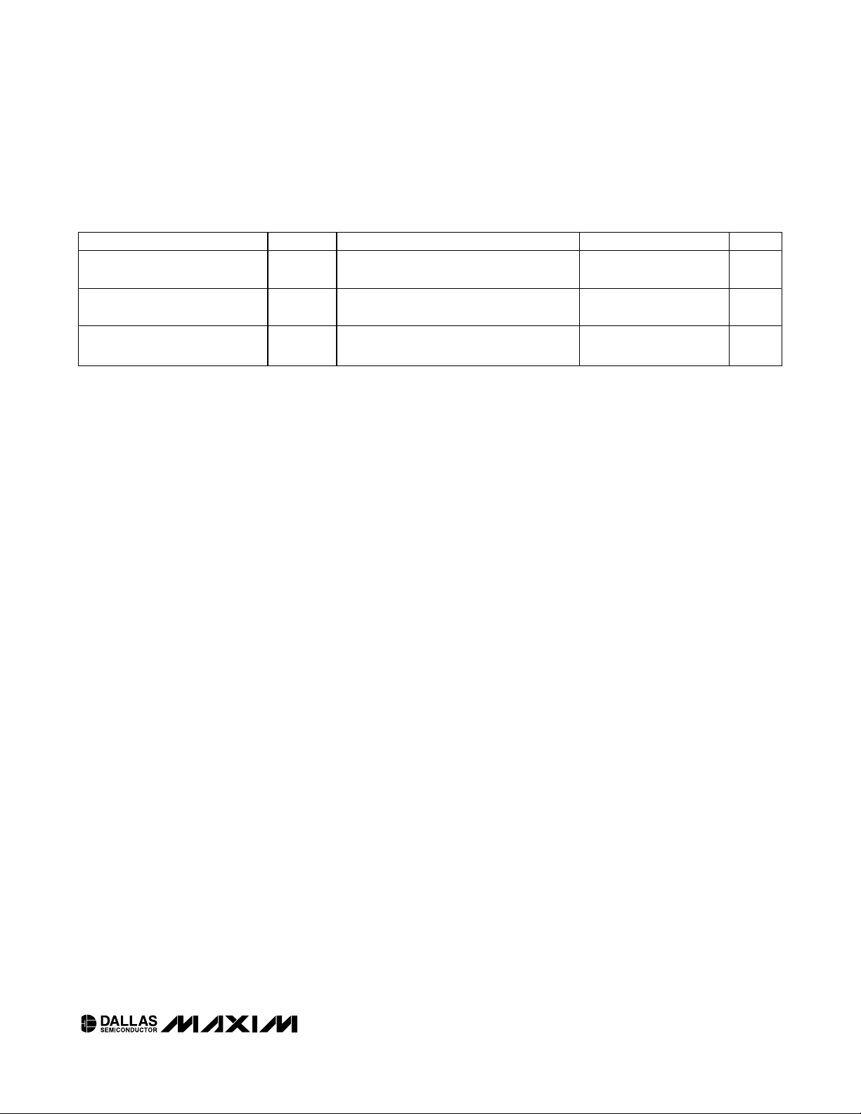
Ordering Information
DS1374
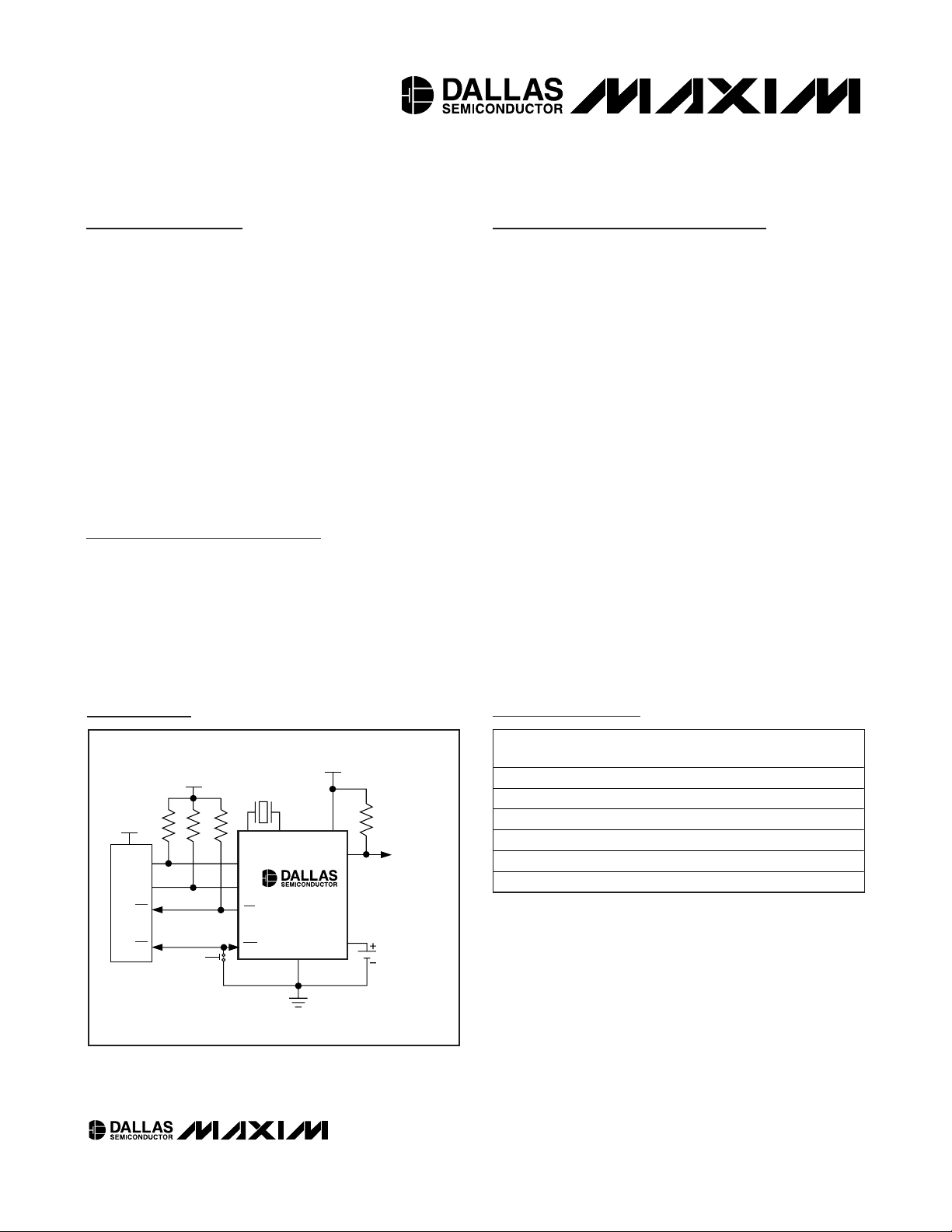
X1 X2
CRYSTAL
V
CC
V
CC
SQW
SCL
SDA
INT
RST
INT
RST
GND
V
BACKUP
V
CC
V
CC
N.O.
PUSHBUTTON
RESET
PRIMARY
BATTERY,
RECHARGEABLE
BATTERY, OR
SUPER CAPACITOR
CPU
RPU
RPU = t
r/CB
RPU
Typical Operating Circuit
Rev 1; 9/04
For pricing, delivery, and ordering information, please contact Maxim/Dallas Direct! at
1-888-629-4642, or visit Maxim’s website at www.maxim-ic.com.
PART
TEMP RANGE
PINPACKAGE
TOP MARK
DS1374U-18
10 µSOP DS1374-18
DS1374U-3
10 µSOP DS1374-3
DS1374U-33
10 µSOP DS1374-33
DS1374C-18
DS1374C-18
DS1374C-3
DS1374C-3
DS1374C-33
DS1374C-33
I2C is a trademark of Philips Corp. Purchase of I2C components of Maxim Integrated Products, Inc., or one of its sublicensed Associated Companies, conveys a license under the
Philips I
2
C Patent Rights to use these components in an I2C
system, provided that the system conforms to the I
2
C Standard
Specification as defined by Philips.
Pin Configurations appear at the end of the data sheet.
-40°C to +85°C
-40°C to +85°C
-40°C to +85°C
-40°C to +85°C 16 SO, 0.300"
-40°C to +85°C 16 SO, 0.300"
-40°C to +85°C 16 SO, 0.300"
Page 2
DS1374
I2C, 32-Bit Binary Counter Watchdog RTC with
Trickle Charger and Reset Input/Output
2 _____________________________________________________________________
ABSOLUTE MAXIMUM RATINGS
RECOMMENDED DC OPERATING CONDITIONS
(VCC= V
CC MIN
to V
CC MAX
, TA= -40°C to +85°C, unless otherwise noted.) (Note 1)
Stresses beyond those listed under “Absolute Maximum Ratings” may cause permanent damage to the device. These are stress ratings only, and functional
operation of the device at these or any other conditions beyond those indicated in the operational sections of the specifications is not implied. Exposure to
absolute maximum rating conditions for extended periods may affect device reliability.
Voltage Range on VCCPin Relative to Ground .....-0.3V to +6.0V
Voltage Range on SDA, SCL, and WDS
Relative to Ground....................................-0.3V to V
CC
+ 0.3V
Operating Temperature Range ...........................-40
°C to +85°C
Storage Temperature Range .............................-55°C to +125°C
Soldering Temperature Range ........................See the Handling,
PC Board Layout, and Assembly section.
PARAMETER
CONDITIONS
UNITS
DS1374-33
3.3
DS1374-3 2.7 3.0 3.3
Supply Voltage
(Notes 2, 3)
V
CC
DS1374-18
1.8
V
Input Logic 1 V
IH
(Note 2)
V
Input Logic 0 V
IL
(Note 2)
+0.3 x
V
Pullup Resistor Voltage (INT,
SQW, SDA, SCL), V
CC
= 0V
V
PU
(Note 2) 5.5 V
DS1374-33
DS1374-3
2.6 2.7
Power-Fail Voltage
(Note 2)
V
PF
DS1374-18
1.6
V
DS1374-33 1.3 3.0
V
CC
DS1374-3 1.3 3.0 3.7
Backup Supply Voltage
(Notes 2, 3, 4)
V
SYMBOL
V
BACKUP
MIN TYP MAX
2.97
1.71
0.7 x V
CC
-0.3
2.70 2.88 2.97
2.45
1.51
V
CC
5.50
1.89
+ 0.3
V
CC
1.71
MAX
Page 3
DS1374
I2C, 32-Bit Binary Counter Watchdog RTC with
Trickle Charger and Reset Input/Output
_____________________________________________________________________ 3
DC ELECTRICAL CHARACTERISTICS
(VCC= V
CC MIN
to V
CC MAX
, TA= -40°C to +85°C, unless otherwise noted.) (Note 1)
PARAMETER
CONDITIONS
UNITS
R1 (Note 5)
R2 (Note 6)
Trickle-Charge Current-Limiting
Resistors
R3 (Note 7)
Ω
Input Leakage I
LI
(Note 8) -1 +1
I/O Leakage I
LO
(Note 9) -1 +1
RST Pin I/O Leakage I
LORST
(Note 10)
+1
µA
SDA Logic 0 Output (V
OL
= 0.4V)
I
OLSDA
3.0 mA
VCC > 2V; VOL = 0.4V 3.0
1.71V < VCC < 2V; VOL = 0.2 V
CC
3.0
mA
RST, SQW, and INT Logic 0
Outputs (Note 11)
I
OL1
1.3V < VCC < 1.71V; VOL = 0.2 V
CC
250 µA
DS1374-18 75 150
DS1374-3
200
Active Supply Current
(Notes 11, 12)
I
CCA
DS1374-33
300
µA
DS1374-18 60 100
DS1374-3 80 125
Standby Current (Notes 11, 13) I
CCS
DS1374-33
175
µA
V
BACKUP
Leakage Current
(V
BACKUP
= 3.7V)
100 nA
DC ELECTRICAL CHARACTERISTICS
(VCC= 0V, V
BACKUP
= 3.7V, TA= -40°C to +85°C, unless otherwise noted.) (Note 1)
PARAMETER
CONDITIONS
UNITS
V
BACKUP
Current (OSC ON);
SQW OFF
(Note 14)
700 nA
V
BACKUP
Current (OSC ON);
SQW ON (32kHz)
(Notes 14, 15)
nA
V
BACKUP
Data-Retention Current
(OSC OFF)
25 100 nA
SYMBOL
I
BACKUPLKG
MIN TYP MAX
250
2000
4000
-200
110
180
115
SYMBOL
I
BKOSC1
I
BKOSC2
I
BACKUPDR
MAX TYP MAX
400
600 1000
Page 4
DS1374
I2C, 32-Bit Binary Counter Watchdog RTC with
Trickle Charger and Reset Input/Output
4 _____________________________________________________________________
AC ELECTRICAL CHARACTERISTICS
(VCC= V
CC MIN
to V
CC MAX
, TA= -40°C to +85°C, unless otherwise noted.) (Note 1) (Figure 1)
PARAMETER
SYMBOL
CONDITIONS
MIN
TYP
MAX
UNITS
Fast mode
400
SCL Clock Frequency (Note 16) f
SCL
Standard mode 0 100
kHz
Fast mode 1.3
Bus Free Time Between STOP
and START Conditions
t
BUF
Standard mode 4.7
µs
Fast mode 0.6
Hold Time (Repeated) START
Condition (Note 17)
Standard mode 4.0
µs
Fast mode 1.3
Low Period of SCL Clock t
LOW
Standard mode 4.7
µs
Fast mode 0.6
High Period of SCL Clock t
HIGH
Standard mode 4.0
µs
Fast mode 0 0.9
Data Hold Time (Notes 18, 19)
Standard mode 0 0.9
µs
Fast mode
Data Setup Time (Note 20)
Standard mode
ns
Fast mode 0.6
Start Setup Time t
SU:STA
Standard mode 4.7
µs
Fast mode 300
Rise Time of Both SDA and SCL
Signals (Note 16)
t
R
Standard mode
20 +
ns
Fast mode 300
Fall Time of Both SDA and SCL
Signals (Note 16)
t
F
Standard mode
20 +
300
ns
Fast mode 0.6
Setup Time for STOP Condition
Standard mode 4.7
µs
C ap aci ti ve Load for E ach Bus Li ne
C
B
(Note 16) 400 pF
I/O C ap aci tance ( S D A, S C L) C
I/O
(Note 21) 10 pF
Pulse Width of Spikes That Must
be Suppressed by the Input Filter
t
SP
Fast mode 30 ns
Pushbutton Debounce PB
DB
(Figure 2)
ms
Reset Active Time t
RST
(Figure 2)
ms
Oscillator Stop Flag (OSF) Delay
t
OSF
(Note 22)
ms
100
t
HD:STA
t
HD:DAT
t
SU:DAT
t
SU:STO
100
250
0.1C
B 1000
0.1C
B
250
250
100
Page 5
DS1374
I2C, 32-Bit Binary Counter Watchdog RTC with
Trickle Charger and Reset Input/Output
_____________________________________________________________________ 5
POWER-UP/POWER-DOWN CHARACTERISTICS
(TA= -40°C to +85°C) (Figure 3)
PARAMETER
CONDITIONS
UNITS
VCC Detect to Recognize Inputs
(V
CC
Rising)
t
RPU
(Note 23)
ms
VCC Fall Time; V
PF(MAX)
to
V
PF(MIN)
t
F
µs
VCC Rise Time; V
PF(MIN)
to
V
PF(MAX)
t
R
0µs
WARNING: Under no circumstances are negative undershoots, of any amplitude, allowed when the device is in write protection.
Note 1: Limits at -40°C are guaranteed by design and not production tested.
Note 2: All voltages are referenced to ground.
Note 3: V
BACKUP
should not exceed V
CC
MAX
or 3.7V, whichever is greater.
Note 4: The use of the 250Ω trickle-charge resistor is not allowed at V
CC
> 3.63V and should not be enabled.
Note 5: Measured at V
CC
= typ, V
BACKUP
= 0V, register 09h = A5h.
Note 6: Measured at V
CC
= typ, V
BACKUP
= 0V, register 09h = A6h.
Note 7: Measured at V
CC
= typ, V
BACKUP
= 0V, register 09h = A7h.
Note 8: SCL only.
Note 9: SDA and SQW and INT.
Note 10: The RST pin has an internal 50kΩ pullup resistor to V
CC
.
Note 11: Trickle charger disabled.
Note 12: I
CCA
—SCL clocking at max frequency = 400kHz.
Note 13: Specified with I
2
C bus inactive.
Note 14: Measured with a 32.768kHz crystal attached to the X1 and X2 pins.
Note 15: WDSTR = 1. BBSQW = 1 is required for operation when V
CC
is below the power-fail trip point (or absent).
Note 16: C
B
—total capacitance of one bus line in pF.
Note 17: After this period, the first clock pulse is generated.
Note 18: The maximum t
HD:DAT
only has to be met if the device does not stretch the low period (t
LOW
) of the SCL signal.
Note 19: A device must internally provide a hold time of at least 300ns for the SDA signal (referred to as the V
IHMIN
of the SCL sig-
nal) to bridge the undefined region of the falling edge of SCL.
Note 20: A fast-mode device can be used in a standard-mode system, but the requirement t
SU:DAT
≥ to 250ns must be met. This is
automatically the case if the device does not stretch the low period of the SCL signal. If such a device does stretch the low
period of the SCL signal, it must output the next data bit to the SDA line t
R
max +
t
SU:DAT
= 1000 + 250 = 1250ns before
the SCL line is released.
Note 21: Guaranteed by design. Not production tested.
Note 22: The parameter t
OSF
is the period of time the oscillator must be stopped for the OSF flag to be set over the voltage range of
0V ≤ V
CC
≤ V
CC MAX
and 1.3V ≤ V
BACKUP
≤ 3.7V.
Note 23: This delay applies only if the oscillator is enabled and running. If the EOSC bit is 1, the startup time of the oscillator is
added to this delay.
SYMBOL
MIN TYP MAX
300
250
Page 6

DS1374
I2C, 32-Bit Binary Counter Watchdog RTC with
Trickle Charger and Reset Input/Output
6 _____________________________________________________________________
OUTPUTS
V
CC
V
PF(MAX)
INPUTS
HIGH-Z
RST
DON'T CARE
VALID
RECOGNIZED
RECOGNIZED
VALID
V
PF(MIN)
t
RST
t
RPU
t
R
t
F
V
PF
V
PF
Figure 3. Power-Up/Power-Down Timing
t
RST
PB
DB
RST
Figure 2. Pushbutton Reset Timing
SDA
SCL
t
HD:STA
t
LOW
t
HIGH
t
R
t
F
t
BUF
t
HD:DAT
t
SU:DAT
REPEATED
START
t
SU:STA
t
HD:STA
t
SU:STO
t
SP
STOP START
Figure 1. Data Transfer on I2C Serial Bus
Page 7

DS1374
I2C, 32-Bit Binary Counter Watchdog RTC with
Trickle Charger and Reset Input/Output
_____________________________________________________________________ 7
I
BAT0SC1
vs. V
BAT
SQUARE-WAVE OFF
DS1374 toc01
V
BAT
(V)
SUPPLY CURRENT (nA)
5.34.84.33.83.32.82.31.8
350
400
450
500
550
300
1.3
VCC = 0V
I
BAT0SC2
vs. V
BAT
SQUARE-WAVE ON
DS1374 toc02
400
450
500
550
600
650
700
750
800
350
VCC = 0V
V
BAT
(V)
SUPPLY CURRENT (nA)
5.34.84.33.83.32.82.31.81.3
I
BATOSC1
vs. TEMPERATURE
V
BAT
= 3.0V
DS1374 toc03
TEMPERATURE (°C)
SUPPLY CURRENT (nA)
806040200-20
400
425
450
475
375
-40
VCC = 0V
I
CCA
vs. V
CC
(SQUARE-WAVE ON)
DS1374 toc04
VCC (V)
SUPPLY CURRENT (µA)
5.34.83.8 4.32.8 3.32.3
75
100
125
150
175
200
225
250
275
50
1.8
OSCILLATOR FREQUENCY vs. V
BACKUP
DS1374 toc05
V
BACKUP
(V)
FREQUENCY (Hz)
5.34.84.33.83.32.82.31.8
32768.3
32768.4
32768.5
32768.6
32768.7
32768.8
32768.2
32768.1
32768.0
1.3
VCC = 0V
VCC FALLING vs. RST DELAY
DS1374 toc06
VCC FALLING (V/ms)
RESET DELAY (µs)
1010.10
1
10
100
1000
0.1
0.01 100
VCC = 3.0V TO 0V
Typical Operating Characteristics
(VCC= +3.3V, TA= +25°C, unless otherwise noted.)
Page 8

DS1374
I2C, 32-Bit Binary Counter Watchdog RTC with
Trickle Charger and Reset Input/Output
8 _____________________________________________________________________
Pin Description
PIN
NAME FUNCTION
1, 2
X1, X2
Connections for a Standard 32.768kHz Quartz Crystal. The internal oscillator circuitry is designed for
operation with a crystal having a specified load capacitance (C
L
) of 6pF. Pin X1 is the input to the
oscillator and can optionally be connected to an external 32.768kHz oscillator. The output of the
internal oscillator, pin X2, is floated if an external oscillator is connected to pin X1.
3
Connection for a Secondary Power Supply. Supply voltage must be held between 1.3V and 3.7V
(-18 and -3) or 1.3V and 5.5V (-33) for proper operation. This pin can be connected to a primary cell
such as a lithium button cell. Additionally, this pin can be connected to a rechargeable cell or a super
cap when used with the trickle-charge feature. UL recognized to ensure against reverse charging
when used with a lithium battery.
4
RST
Active-Low, Open-Drain Output with a Debounced Pushbutton Input. This pin can be activated by a
pushbutton reset request, a watchdog alarm condition, or a power-fail event. It has an internal 50kΩ
pullup resistor.
5
GND Ground
6
SDA
Serial Data Input/Output. SDA is the input/output for the 2-wire serial interface. The SDA pin is open
drain and requires an external pullup resistor.
71SCL
Serial Clock Input. SCL is the clock input for the 2-wire serial interface and is used to synchronize
data movement on the serial interface.
82 INT
Interupt. This pin is used to output the alarm interrupt or the watchdog reset signal. It is active-low
open drain and requires an external pullup resistor.
93SQW
Square-Wave Output. This pin is used to output the programmable square-wave signal. It is open
drain and requires an external pullup resistor.
10 4 V
CC
DC Power for Primary Power Supply
—
N.C. No Connection. Must be connected to ground.
Figure 4. Functional Diagram
µSOP SO
—
13 V
BACKUP
14
15
16
5–12
X1
X2
V
CC
V
BACKUP
GND
SDA
SCL
CLOCK
DIVIDER
POWER
CONTROL
AND
TRICKLE
CHARGE
2-WIRE
INTERFACE
1Hz
4.096kHz
8.192kHz
32.768kHz
32-BIT
COUNTER
ALARM/
WATCHDOG
STAT/CTRL/
TRICKLE
MUX
DS1374
1Hz/0.96kHz
24-BIT
COUNTER
INT
CONTROL
RST
CONTROL
SQW
INT
RST
Page 9

Detailed Description
The DS1374 is a real-time clock with an I2C serial interface. It provides elapsed seconds from a user-defined
starting point in a 32-bit counter (Figure 4). A 24-bit
counter can be configured as either a watchdog
counter or an alarm counter. An on-chip oscillator circuit uses a customer-supplied 32.768kHz crystal to
keep time. A power-control circuit switches operation
from VCCto V
BACKUP
and back when power on VCCis
cycled. If a rechargeable backup supply is used, a
trickle charger can be enabled to charge the backup
supply while VCCis on.
Oscillator Circuit
The DS1374 uses an external 32.768kHz crystal. The
oscillator circuit does not require any external resistors
or capacitors to operate. Table 1 specifies several crystal parameters for the external crystal. Figure 5 shows a
functional schematic of the oscillator circuit. The startup
time is usually less than 1 second when using a crystal
with the specified characteristics.
Clock Accuracy
Clock accuracy is dependent upon the accuracy of the
crystal and the accuracy of the match between the
capacitive load of the oscillator circuit and the capacitive
load for which the crystal was trimmed. Additional error
is added by crystal frequency drift caused by temperature shifts. External circuit noise coupled into the oscillator circuit can result in the clock running fast. Figure 6
shows a typical PC board layout for isolating the crystal
and oscillator from noise. Refer to Application Note 58:
Crystal Considerations with Dallas Real-Time Clocks for
detailed information.
DS1374C Only
The DS1374C integrates a standard 32,768Hz crystal
into the package. Typical accuracy at nominal VCCand
25°C is approximately 10ppm. See Application Note 58
for information about crystal accuracy vs. temperature.
Address Map
Table 2 shows the address map for the DS1374 registers. During a multibyte access, the address pointer
wraps around to location 00h when it reaches the end of
the register space (08h). On an I2C START, STOP, or
address pointer incrementing to location 00h, the current
time is transferred to a second set of registers. These
secondary registers read the time information, while the
clock continues to run. This eliminates the need to reread
the registers in case of an update of the main registers
during a read.
Time-of-Day Counter
The time-of-day counter is a 32-bit up counter. The
contents can be read or written by accessing the
DS1374
I2C, 32-Bit Binary Counter Watchdog RTC with
Trickle Charger and Reset Input/Output
_____________________________________________________________________ 9
COUNTDOWN
CHAIN
X1
X2
C
L
1
C
L
2
CRYSTAL
RTC
REGISTERS
DS1374
Figure 5. Oscillator Circuit Showing Internal Bias Network
LOCAL GROUND PLANE (LAYER 2)
NOTE: AVOID ROUTING SIGNALS IN THE CROSSHATCHED AREA (UPPER LEFT-HAND
QUADRANT) OF THE PACKAGE UNLESS THERE IS A GROUND PLANE BETWEEN THE
SIGNAL LINE AND THE PACKAGE.
CRYSTAL
GND
X2
X1
Figure 6. Layout Example
PARAMETER
TYP
UNITS
Nominal
Frequency
f
O
kHz
Series
Resistance
ESR 45 kΩ
Load
Capacitance
C
L
6pF
Table 1. Crystal Specifications*
*The crystal, traces, and crystal input pins should be isolated
from RF generating signals. Refer to Application Note 58:
Crystal Considerations for Dallas Real-Time Clocks for additional specifications.
SYMBOL MIN
MAX
32.768
Page 10

DS1374
address range 00h–03h. When the counter is read, the
current time of day is latched into a register, which is
output on the serial data line while the counter continues to increment.
Watchdog/Alarm Counter
The contents of the watchdog/alarm counter, which is a
separate 24-bit down counter, are accessed in the
address range 04h–06h. When this counter is written, the
counter and a seed register are loaded with the desired
value. When the counter is to be reloaded, it uses the
value in the seed register. When the counter is read, the
current counter value is latched into a register, which is
output on the serial data line while the counter continues
to decrement.
If the counter is not needed, it can be disabled and used
as a 24-bit cache of NV RAM by setting the WACE bit in
the control register to logic 0. If all 24 bits of the watchdog/alarm counter are written to zero when
WACE = 1, the counter is disabled and the AF bit is
not set.
When the WD/ALM bit in the control register is set to a
logic 0, the WD/ALM counter decrements every second
until it reaches zero. At this point, the AF bit in the status
register is set and the counter is reloaded and restarted.
If AF is set when the watchdog function is enabled, the
output selected by WDSTR immediately becomes active.
When the WD/ALM bit is set to logic 1, the WD/ALM
counter decrements every 1/4096 of a second (approximately every 244µs) until it reaches zero, sets the AF bit
in the status register, and stops. If WDSTR = 0, the RST
pin pulses low for 250ms, and accesses to the DS1374
are inhibited. At the end of the 250ms pulse, the AF bit is
cleared to zero, the RST pin becomes high impedance,
and read/write access to the DS1374 is enabled. If AIE =
1 and WDSTR = 1, the INT pin pulses low for 250ms. The
pulse cannot be truncated by writing either AF or AIE to
zero during the low time of the INT pin. If the WD/ALM
counter is written during the 250ms pulse, the counter
starts decrementing upon the pulse completion. At the
completion, the AF bit clears to zero and the INT pin
becomes high impedance. The WD/ALM counter can be
reloaded and restarted before the counter reaches zero
by reading or writing any of the WD/ALM counter regis-
ters.
Power-Up/Power-Down Reset and
Pushbutton Reset Functions
A precision temperature-compensated reference and
comparator circuit monitors the status of VCC. When an
out-of-tolerance condition occurs, an internal power-fail
signal is generated that forces the RST pin low and
blocks read/write access to the DS1374. When V
CC
returns to an in-tolerance condition, the RST pin is held
low for 250ms to allow the power supply to stabilize. If
the EOSC bit is set to a logic 1 (to disable the oscillator in
battery-backup mode), the reset signal is kept active for
250ms plus the startup time of the oscillator.
The DS1374 provides for a pushbutton switch to be connected to the RST output pin. When the DS1374 is not in
a reset cycle, it continuously monitors the RST signal for
a low-going edge. If an edge is detected, the DS1374
debounces the switch by pulling the RST pin low and
inhibits read/write access. After the internal 250ms timer
has expired, the device continues to monitor the RST
line. If the line is still low, the DS1374 continues to monitor the line, looking for a rising edge. Upon detecting
release, the DS1374 forces the RST pin low and holds it
low for an additional 250ms.
I2C, 32-Bit Binary Counter Watchdog RTC with
Trickle Charger and Reset Input/Output
10 ____________________________________________________________________
ADDRESS
BIT 7 BIT 6 BIT 5 BIT 4 BIT 3 BIT 2 BIT 1 BIT 0 FUNCTION
00H TOD Counter Byte 0 Time-of-Day Counter
01H TOD Counter Byte 1 Time-of-Day Counter
02H TOD Counter Byte 2 Time-of-Day Counter
03H TOD Counter Byte 3 Time-of-Day Counter
04H WD/ALM Counter Byte 0
Watchdog/Alarm Counter
05H WD/ALM Counter Byte 1
Watchdog/Alarm Counter
06H WD/ALM Counter Byte 2
Watchdog/Alarm Counter
07H
RS2 RS1 AIE Control
08H OSF 0 0 0 0 0 0 AF Status
09H TCS3 TCS2 TCS1 TCS0 DS1 DS0
Trickle Charger
Table 2. Address Map
Note: Unless otherwise specified, the state of the registers is not defined when power is first applied.
EOSC WACE WD/ALM BBSQW WDSTR
ROUT1 ROUT0
Page 11

Special Purpose Registers
The DS1374 has two additional registers (07h–08h) that
control the WD/ALM counter and the square-wave, interrupt, and reset outputs.
Control Register (07h)
Bit 7/Enable Oscillator (EOSC). When set to logic 0,
the oscillator is started. When set to logic 1, the oscillator is stopped. When this bit is set to logic 1, the oscillator is stopped and the DS1374 is placed into a
low-power standby mode (I
DDR
). This bit is clear (logic
0) when power is first applied. When the DS1374 is
powered by VCC, the oscillator is always on regardless
of the state of the EOSC bit.
Bit 6/WD/
AALLMM
Counter Enable (WACE). When set to
logic 1, the WD/ALM counter is enabled. When set to
logic 0, the WD/ALM counter is disabled, and the 24
bits can be used as NV RAM. This bit is clear (logic 0)
when power is first applied.
Bit 5/WD/
AALLMM
Counter Select (WD/ALM). When set to
logic 0, the counter decrements every second until it
reaches zero and is then reloaded and restarted. When
set to logic 1, the WD/ALM counter decrements every
1/4096 of a second (approximately every 244µs) until it
reaches zero, sets the AF bit in the status register, and
stops. If any of the WD/ALM counter registers are
accessed before the counter reaches zero, the counter
is reloaded and restarted. This bit is clear (logic 0)
when power is first applied.
Bit 4/Battery-Backed Square-Wave Enable (BBSQW).
This bit, when set to logic 1, enables the square-wave
output when V
CC
is absent and when the DS1374 is
being powered by the V
BACKUP
pin. When BBSQW is
logic 0, the SQW pin goes high impedance when V
CC
falls below the power-fail trip point. This bit is disabled
(logic 0) when power is first applied.
Bit 3/Watchdog Reset Steering Bit (WDSTR). This bit
selects which output pin the watchdog-reset signal
occurs on. When the WDSTR bit is set to logic 0, a
250ms pulse occurs on the RST pin if WD/ALM = 1 and
the WD/ALM counter reaches zero. The 250ms reset
pulse occurs on the INT pin when the WDSTR bit is set
to logic 1. This bit is logic 0 when power is first applied.
Bits 2, 1/Rate Select (RS2 and RS1). These bits control the frequency of the square-wave output when the
square wave has been enabled. Table 3 shows the
square-wave frequencies that can be selected with the
RS bits. These bits are both set (logic 1) when power is
first applied.
Bit 0/Alarm Interrupt Enable (AIE). When set to logic
1, this bit permits the alarm flag (AF) bit in the status
register to assert INT (when INTCN = 1). When set to
logic 0 or INTCN is set to logic 0, the AF bit does not
initiate the INT signal. If the WD/ALM bit is set to logic 1
and the AF flag is set, writing AIE to zero does not truncate the 250ms pulse on the INT pin. The AIE bit is at
logic 0 when power is first applied. The INT output is
available while the device is powered by either supply.
DS1374
I2C, 32-Bit Binary Counter Watchdog RTC with
Trickle Charger and Reset Input/Output
____________________________________________________________________ 11
TCS3 TCS2 TCS1 TCS0 DS1 DS0
FUNCTION
XXXX00XXDisabled
XXXX11XXDisabled
XXXXXX00Disabled
10100101No diode, 250Ω resistor
10101001One diode, 250Ω resistor
10100110No diode, 2kΩ resistor
10101010One diode, 2kΩ resistor
10100111No diode, 4kΩ resistor
10101011One diode, 4kΩ resistor
00000000Power-on reset value
Table 4. Trickle Charge Register
Bit 7 Bit 6 Bit 5 Bit 4 Bit 3 Bit 2 Bit 1 Bit 0
EOSC WACE WD/ALM BBSQW WDSTR RS2 RS1 AIE
ROUT1 ROUT0
Page 12

DS1374
Status Register (08h)
Bit 7/Oscillator Stop Flag (OSF). A logic 1 in this bit
indicates that the oscillator either is stopped or was
stopped for some period of time and can be used to
judge the validity of the timekeeping data. This bit is set
to logic 1 any time the oscillator stops. The following
are examples of conditions that can cause the OSF bit
to be set:
1) The first time power is applied.
2) The voltage present on VCCis insufficient to support
oscillation.
3) The EOSC bit is turned off.
4) External influences on the crystal (i.e., noise, leakage, etc.).
This bit remains at logic 1 until written to logic 0.
Bit 0/Alarm Flag (AF). A logic 1 in the alarm flag bit
indicates that the WD/ALM counter reached zero. If
WD/ALM is set to zero and the AIE bit = 1, the INT pin
goes low and stays low until AF is cleared. AF is
cleared when written to logic 0. This bit can only be
written to logic 0. Attempting to write logic 1 leaves the
value unchanged. If WD/ALM is set to 1 and the AIE
bit = 1, the INT pin pulses low for 250ms when the
WD/ALM counter reaches zero and sets AF = 1. At the
pulse completion, the DS1374 clears the AF bit to zero.
If the 250ms pulse is active, writing AF to zero does not
truncate the pulse.
Trickle-Charge Register (10h)
The simplified schematic in Figure 7 shows the basic
components of the trickle charger. The trickle-charge
select (TCS) bits (bits 4–7) control the selection of the
trickle charger. To prevent accidental enabling, only a
pattern of 1010 enables the trickle charger. All other
patterns disable the trickle charger. The trickle charger
is disabled when power is first applied. The diode
select (DS) bits (bits 2, 3) select whether or not a diode
is connected between VCCand V
BACKUP
. If DS is 01,
no diode is selected; if DS is 10, a diode is selected.
The ROUT bits (bits 0, 1) select the value of the resistor
connected between VCCand V
BACKUP
. Table 4 shows
the resistor selected by the resistor select (ROUT) bits
and the diode selected by the diode select (DS) bits.
Warning: The ROUT value of 250Ω must not be select-
ed whenever VCCis greater than 3.63V.
The user determines diode and resistor selection
according to the maximum current desired for battery or
super cap charging. The maximum charging current can
be calculated as illustrated in the following example.
I2C, 32-Bit Binary Counter Watchdog RTC with
Trickle Charger and Reset Input/Output
12 ____________________________________________________________________
BIT 7
TCS3
1 OF 16 SELECT
NOTE: ONLY 1010b
ENABLES CHARGER
1 OF 2
SELECT
V
CC
V
BACKUP
R1
250Ω
TCS
0-3
= TRICKLE CHARGER SELECT
DS
0-1
= DIODE SELECT
TOUT
0-1
= RESISTOR SELECT
R2
2kΩ
R3
4kΩ
1 OF 3
SELECT
BIT 6
TCS2
BIT 5
TCS1
BIT 4
TCS0
BIT 3
DS1
BIT 2
DS0
BIT 1
ROUT1
BIT 0
ROUT0
Figure 7. Programmable Trickle Charger
Bit 7 Bit 6 Bit 5 Bit 4 Bit 3 Bit 2 Bit 1 Bit 0
OSF 0 0 0000AF
Table 3. Square-Wave Output Frequency
RS2 RS1 SQUARE-WAVE OUTPUT FREQUENCY
00 1Hz
01 4.096kHz
10 8.192kHz
11 32.768kHz
Page 13

Assume that a system power supply of 3.3V is applied
to VCCand a super cap is connected to V
BACKUP
. Also
assume the trickle charger has been enabled with a
diode and resistor R2 between VCCand V
BACKUP
. The
maximum current I
MAX
would therefore be calculated
as follows:
I
MAX
= (3.3V - diode drop) / R2 ≈ (3.3V - 0.7V) / 2kΩ≈
1.3mA
As the super cap changes, the voltage drop between
VCCand V
BACKUP
decreases and therefore the charge
current decreases.
I2C Serial Data Bus
The DS1374 supports the I2C bus protocol. A device
that sends data onto the bus is defined as a transmitter
and a device receiving data is a receiver. The device
that controls the message is called a master. The
devices that are controlled by the master are slaves. A
master device that generates the serial clock (SCL),
controls the bus access, and generates the START and
STOP conditions must control the bus. The DS1374
operates as a slave on the I2C bus. Connections to the
bus are made through the open-drain I/O lines SDA
and SCL. A standard mode (100kHz max clock rate)
and a fast mode (400kHz max clock rate) are defined
within the bus specifications. The DS1374 works in both
modes.
The following bus protocol has been defined (Figure 8):
• Data transfer can be initiated only when the bus is
not busy.
• During data transfer, the data line must remain sta-
ble whenever the clock line is high. Changes in the
data line while the clock line is high can be interpreted as control signals.
Accordingly, the following bus conditions have been
defined:
Bus not busy: Both data and clock lines remain
high.
Start data transfer: A change in the state of the
data line from high to low, while the clock line is
high, defines a START condition.
Stop data transfer: A change in the state of the
data line from low to high, while the clock line is
high, defines a STOP condition.
Data valid: The state of the data line represents
valid data when, after a START condition, the data
line is stable for the duration of the high period of
the clock signal. The data on the line must be
changed during the low period of the clock signal.
There is one clock pulse per bit of data.
Each data transfer is initiated with a START condition and terminated with a STOP condition. The
number of data bytes transferred between the
START and the STOP conditions is not limited, and
is determined by the master device. The information is transferred byte-wise and each receiver
acknowledges with a ninth bit. A standard mode
(100kHz clock rate) and a fast mode (400kHz clock
rate) are defined within the I
2
C bus specifications.
Acknowledge: Each receiving device, when
addressed, is obliged to generate an acknowledge
after the reception of each byte. The master device
must generate an extra clock pulse that is associated with this acknowledge bit.
DS1374
I2C, 32-Bit Binary Counter Watchdog RTC with
Trickle Charger and Reset Input/Output
____________________________________________________________________ 13
STOP
CONDITION
OR REPEATED
START
CONDITION
REPEATED IF MORE BYTES
ARE TRANSFERED
ACK
START
CONDITION
ACK
ACKNOWLEDGEMENT
SIGNAL FROM RECEIVER
ACKNOWLEDGEMENT
SIGNAL FROM RECEIVER
SLAVE ADDRESS
MSB
SCL
SDA
R/W
DIRECTION
BIT
12 678 9 12 893–7
Figure 8. I2C Data Transfer Overview
Page 14

DS1374
I2C, 32-Bit Binary Counter Watchdog RTC with
Tickle Charger and Reset Input/Output
14 ____________________________________________________________________
A device that acknowledges must pull down the
SDA line during the acknowledge clock pulse in
such a way that the SDA line is stable low during
the high period of the acknowledge-related clock
pulse. Setup and hold times must be considered. A
master must signal an end of data to the slave by
not generating an acknowledge bit on the last byte
that has been clocked out of the slave. In this case,
the slave must leave the data line high to enable
the master to generate the STOP condition.
Figures 9 and 10 detail how data transfer is accomplished on the 2-wire bus. Depending on the state of
the R/W bit, two types of data transfer are possible:
Data transfer from a master transmitter to a
slave receiver. The first byte transmitted by the
master is the slave address. Next follows a number
of data bytes. The slave returns an acknowledge bit
after each received byte.
Data transfer from a slave transmitter to a master receiver. The master transmits the first byte (the
slave address). The slave then returns an acknowledge bit. Next follows a number of data bytes
transmitted by the slave to the master. The master
returns an acknowledge bit after all received bytes
other than the last byte. At the end of the last
received byte, a “not acknowledge” is returned.
The master device generates the serial clock pulses and the START and STOP conditions. A transfer
is ended with a STOP condition or with a repeated
START condition. Since a repeated START condition is also the beginning of the next serial transfer,
the bus is not released.
The DS1374 can operate in the following two modes:
Slave Receiver Mode (Write Mode): Serial data
and clock data are received through SDA and SCL.
After each byte is received, an acknowledge bit is
transmitted. START and STOP conditions are recognized as the beginning and end of a serial transfer. Address recognition is performed by hardware
after reception of the slave address and direction
bit. The slave address byte is the first byte received
after the master generates a START condition. The
slave address byte contains the 7-bit DS1374
address, which is 1101000, followed by the direction bit (R/W), which is zero for a write. After receiv-
ing and decoding the slave address byte, the
DS1374 outputs an acknowledge on SDA. After the
DS1374 acknowledges the slave address + write
bit, the master transmits a register address to the
DS1374. This sets the register pointer on the
DS1374, with the DS1374 acknowledging the transfer. The master can then transmit zero or more
bytes of data, with the DS1374 acknowledging
each byte received. The register pointer increments
after each data byte is transferred. The master generates a STOP condition to terminate the data write.
Slave Transmitter Mode (Read Mode): The first
byte is received and handled as in the slave receiver mode. However, in this mode, the direction bit
indicates that the transfer direction is reversed.
Serial data is transmitted on SDA by the DS1374,
while the serial clock is input on SCL. START and
STOP conditions are recognized as the beginning
and end of a serial transfer. Address recognition is
performed by hardware after reception of the slave
address and direction bit. The slave address byte
is the first byte received after the START condition
is generated by the master. The slave address byte
contains the 7-bit DS1374 address, which is
1101000, followed by the direction bit (R/W), which
is 1 for a read. After receiving and decoding the
slave address byte, the DS1374 outputs an
acknowledge on SDA. The DS1374 then begins to
transmit data starting with the register address
pointed to by the register pointer. If the register
pointer is not written to before the initiation of a
read mode, the first address that is read is the last
one stored in the register pointer. The DS1374 must
receive a not acknowledge to end a read.
S 1101000 0 A XXXXXXXX A XXXXXXXX A XXXXXXXX A XXXXXXXX P
DATA TRANSFERRED
(X+1 Bytes + Acknowledge)
SLAVE
ADDRESS
S - START
A - ACKNOWLEDGE
P - STOP
R/W - READ/WRITE OR
DIRECTION BIT
DATA (n)
REGISTER
ADDRESS (n) DATA (n + 1) DATA (n + x)
R/W
Figure 9. I2C Write Protocol
S 1101000 1 A XXXXXXXX A XXXXXXXX A XXXXXXXX A XXXXXXXX /A
DATA TRANSFERRED
(X+1 Bytes + Acknowledge)
SLAVE
ADDRESS
S - START
A - ACKNOWLEDGE
P - STOP
/A - NOT ACKNOWLEDGE
R/W - READ/WRITE OR
DIRECTION BIT
DATA (n) DATA (n + 1) DATA (n + x)DATA (n + 2)
R/W
Figure 10. I2C Read Protocol
Page 15

Handling, PC Board Layout, and
Assembly
The DS1374C package contains a quartz tuning-fork
crystal. Pick-and-place equipment can be used, but
precautions should be taken to ensure that excessive
shocks are avoided. Ultrasonic cleaning should be
avoided to prevent damage to the crystal.
Avoid running signal traces under the package, unless
a ground plane is placed between the package and
the signal line. All no connect (N.C.) pins must be connected to ground.
The SO package can be reflowed as long as the peak
temperature does not exceed 240°C. Peak reflow temperature (≥ 230°C) duration should not exceed 10 seconds, and the total time above 200°C should not
exceed 40 seconds (30 seconds nominal). Exposure to
reflow is limited to 2 times maximum.
Moisture-sensitive packages are shipped from the factory dry-packed. Handling instructions listed on the
package label must be followed to prevent damage
during reflow. Refer to the IPC/JEDEC J-STD-020B standard for moisture-sensitive device (MSD) classifications.
Chip Information
TRANSISTOR COUNT: 11,036
PROCESS: CMOS
SUBSTRATE CONNECTED TO GROUND
Thermal Information
Theta-JA: 221°C/W (µSOP)
Theta-JC: 39°C/W (µSOP)
Theta-JA: 73°C/W (16 SO)
Theta-JC: 23°C/W (16 SO)
DS1374
I2C, 32-Bit Binary Counter Watchdog RTC with
Tickle Charger and Reset Input/Output
Maxim cannot assume responsibility for use of any circuitry other than circuitry entirely embodied in a Maxim product. No circuit patent licenses are
implied. Maxim reserves the right to change the circuitry and specifications without notice at any time.
Maxim Integrated Products, 120 San Gabriel Drive, Sunnyvale, CA 94086 408-737-7600 ____________________ 15
© 2004 Maxim Integrated Products Printed USA is a registered trademark of Maxim Integrated Products.
is a registered trademark of Dallas Semiconductor Corporation.
Package Information
(For the latest package outline information, go to
www.maxim-ic.com/DallasPackInfo.)
1
2
3
4
5
10
9
8
7
6
V
CC
SQW
INT
SCLRST
V
BACKUP
X2
X1
TOP VIEW
SDAGND
DS1374
µSOP
SCL 1
2
3
4
5
6
7
8
16
15
14
13
12
11
10
9
SDA
GND
V
BACKUP
INT
V
CC
SQW
N.C.
N.C.
N.C.
N.C.
RST
N.C.
N.C.
N.C.
N.C.
SO (0.300")
DS1374C
Pin Configurations
 Loading...