

Page 1
19-4998; Rev 0; 10/09
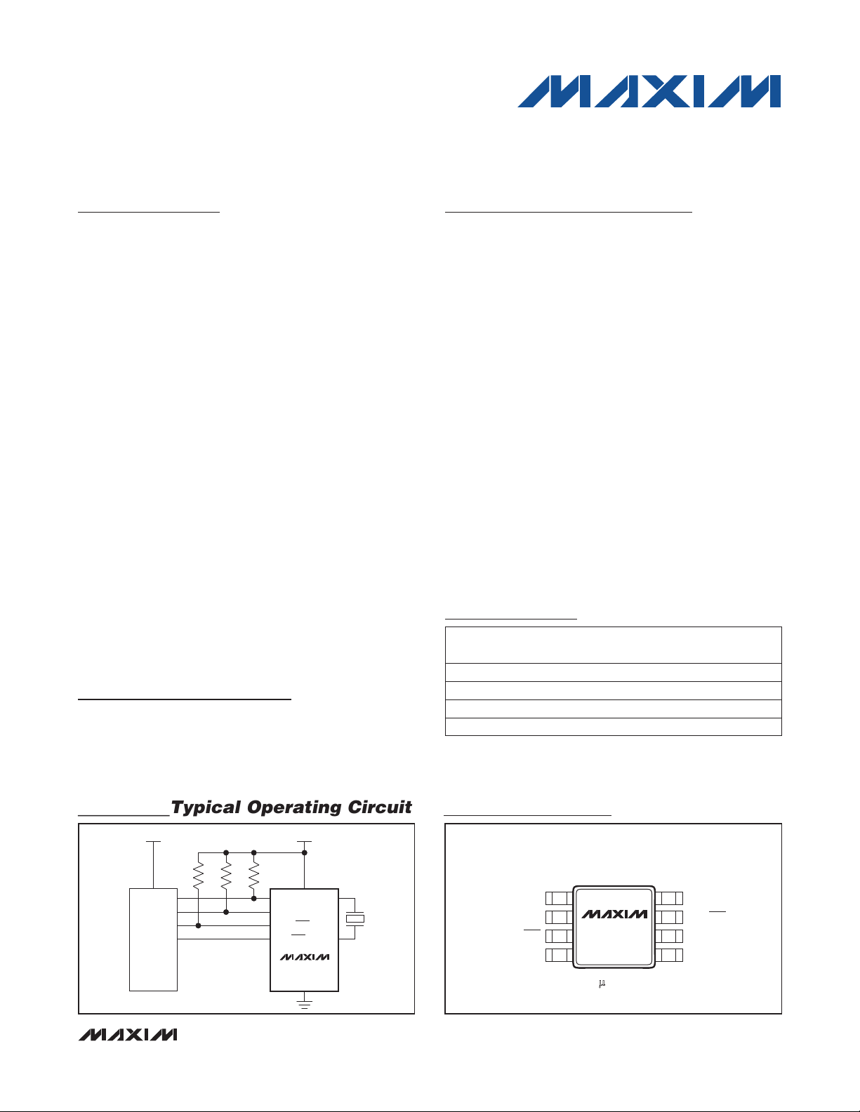
Typical Operating Circuit
Low-Current I2C RTCs for High-ESR Crystals
General Description
The DS1341/DS1342 low-current real-time clocks (RTCs)
are timekeeping devices that provide an extremely low
standby current, which permits longer life from a power
supply. The DS1341/DS1342 support high-ESR crystals,
which broaden the pool of usable crystals for the devices.
The DS1341 uses a 6pF crystal, while the DS1342 uses a
12.5pF crystal. These devices are accessed through an
I2C serial interface. Other features include two time-of-day
alarms, two interrupt outputs, a programmable squarewave output, and a serial bus timeout mechanism.
The clock/calendar provides seconds, minutes, hours,
day, date, month, and year information. The date at the
end of the month is automatically adjusted for months
with fewer than 31 days, including corrections for leap
year. The clock operates in either 24hr or 12hr format
with an AM/PM indicator.
The DS1341/DS1342 also include an input for synchronization. When a reference clock (e.g., 60Hz power line or
GPS 1PPS) is present at the CLKIN pin and the enable
external clock input bit (ECLK) is set to 1, the DS1341/
DS1342 RTCs are frequency-locked to the external clock
and the clock accuracy is determined by the external
source. In case of external clock failure, the clock is
switched to the crystal oscillator.
The devices are available in a lead(Pb)-free/RoHScompliant, 8-pin FSOP package. The devices support a
-40NC to +85NC extended temperature range.
Applications
Medical
Point of Sale (POS)
Telematics
Portable Instruments
Portable Audio
Automotive
Features
S Low Timekeeping Current of 250nA (typ)
S Compatible with Crystal ESR Up to 80kI
S Use Crystals with C
= 6pF (DS1341) or
L
CL = 12.5pF (DS1342)
S +1.8V to +5.5V Operating Voltage Range
S Maintain Time Down to +1.15V (typ)
S Fast (400kHz) I
S Bus Timeout for Lockup-Free Operation
S RTC Counts Seconds, Minutes, Hours, Day, Date,
2
C Interface
Month, and Year with Leap Year Compensation
Valid Through 2099
S External Clock Source for Synchronization Clock
Reference (e.g., 32kHz, 50Hz/60Hz Power Line,
GPS 1PPS)
S Two Time-of-Day Alarms with Two Interrupt
Outputs
S Programmable Square-Wave Output
S Industrial Temperature Range
S Small, 8-Pin µSOP Package
Ordering Information
PART TEMP RANGE
DS1341U+
DS1341U+T&R
DS1342U+*
DS1342U+T&R*
+Denotes a lead(Pb)-free/RoHS-compliant package.
T&R = Tape and reel.
*Future product—contact factory for availability.
-40NC to +85NC 8 FSOP
-40NC to +85NC 8 FSOP
-40NC to +85NC 8 FSOP
-40NC to +85NC 8 FSOP
PINPACKAGE
OSC
CL (pF)
6
6
12.5
12.5
DS1341/DS1342
V
CC
R
R
R
PU
CPU
_______________________________________________________________ Maxim Integrated Products 1
PU
PU
V
CC
V
CC
SCL
SDA
CLKIN/INTA
SQW/INTBX1X2
DS1341/DS1342
GND
For pricing, delivery, and ordering information, please contact Maxim Direct at 1-888-629-4642,
or visit Maxim’s website at www.maxim-ic.com.
Pin Configuration
TOP VIEW
+
1 8 V
X1
2 7 SQW/INTBX2
DS1341
DS1342
µSOP
CC
SCLCLKIN/INTA 3 6
SDAGND 4 5
Page 2
Low-Current I2C RTCs for High-ESR Crystals
ABSOLUTE MAXIMUM RATINGS
Voltage Range on Any Pin Relative to Ground ....-0.3V to +6.0V
Operating Temperature Range .......................... -40NC to +85NC
Junction-to-Ambient Thermal
Resistance (BJA) (Note 1) ........................................ +221NC/W
Junction-to-Case Thermal
Resistance (BJC) (Note 1) ......................................... +39NC/W
Note 1: Package thermal resistances were obtained using the method described in JEDEC specification JESD51-7, using a four-
layer board. For detailed information on package thermal considerations, refer to www.maxim-ic.com/thermal-tutorial.
Stresses beyond those listed under “Absolute Maximum Ratings” may cause permanent damage to the device. These are stress ratings only, and functional
operation of the device at these or any other conditions beyond those indicated in the operational sections of the specifications is not implied. Exposure to absolute
maximum rating conditions for extended periods may affect device reliability.
Junction Temperature Maximum .....................................+150NC
Storage Temperature Range ............................ -55NC to +125NC
Soldering Temperature .........................Refer to the IPC/JEDEC
J-STD-020 Specification.
DS1341/DS1342
DC ELECTRICAL CHARACTERISTICS
(VCC = +1.8V to +5.5V, TA = -40NC to +85NC, unless otherwise noted.) (Note 2)
PARAMETER SYMBOL CONDITIONS MIN TYP MAX UNITS
Operating Voltage Range
Minimum Timekeeping Voltage V
Timekeeping Current: DS1341
CLKIN = GND or CLKIN = VCC
(Note 4)
Logic 1 Input V
Logic 0 Input V
Input Leakage
(SCL, CLKIN/INTA)
Output Leakage
(CLKIN/INTA, SQW/INTB)
Output Logic 1
VOH = +1.0V (SQW /INTB)
Output Logic 0
VOL = +0.4V (SDA, CLKIN/INTA,
SQW/INTB)
V
CCTMIN
I
V
CCT
CCT
I
I
I
OH
I
OL
CC
LI
O
Full operation (Note 3) 1.8 5.5
Timekeeping (Notes 3, 4) 1.3 5.5
TA = +25NC (Notes 3, 4)
VCC = +3.0V, EGFIL = 0, DOSF = 1 220 500
VCC = +5.5V 250 600
VCC = +3.0V, EGFIL = 1, DOSF = 0 280 560
VCC = +5.5V 320 700
(Note 2)
IH
(Note 2) -0.3
IL
ECLK = 1, VIN = 0V to V
ECLK = A1IE = A2IE = 0 -1.0 +1.0
VCC R 1.8V, INTCN = 0
VCC R 1.3V, INTCN = 0
VCC R 1.8V
VCC R 1.3V (Note 5)
CC
0.7 x
V
CC
-0.1 +0.1
-3.0 mA
-250
3.0 mA
250
1.15 1.3 V
VCC +
0.3
0.3 x
V
CC
V
nA
V
V
FA
FA
FA
FA
2
Page 3
Low-Current I2C RTCs for High-ESR Crystals
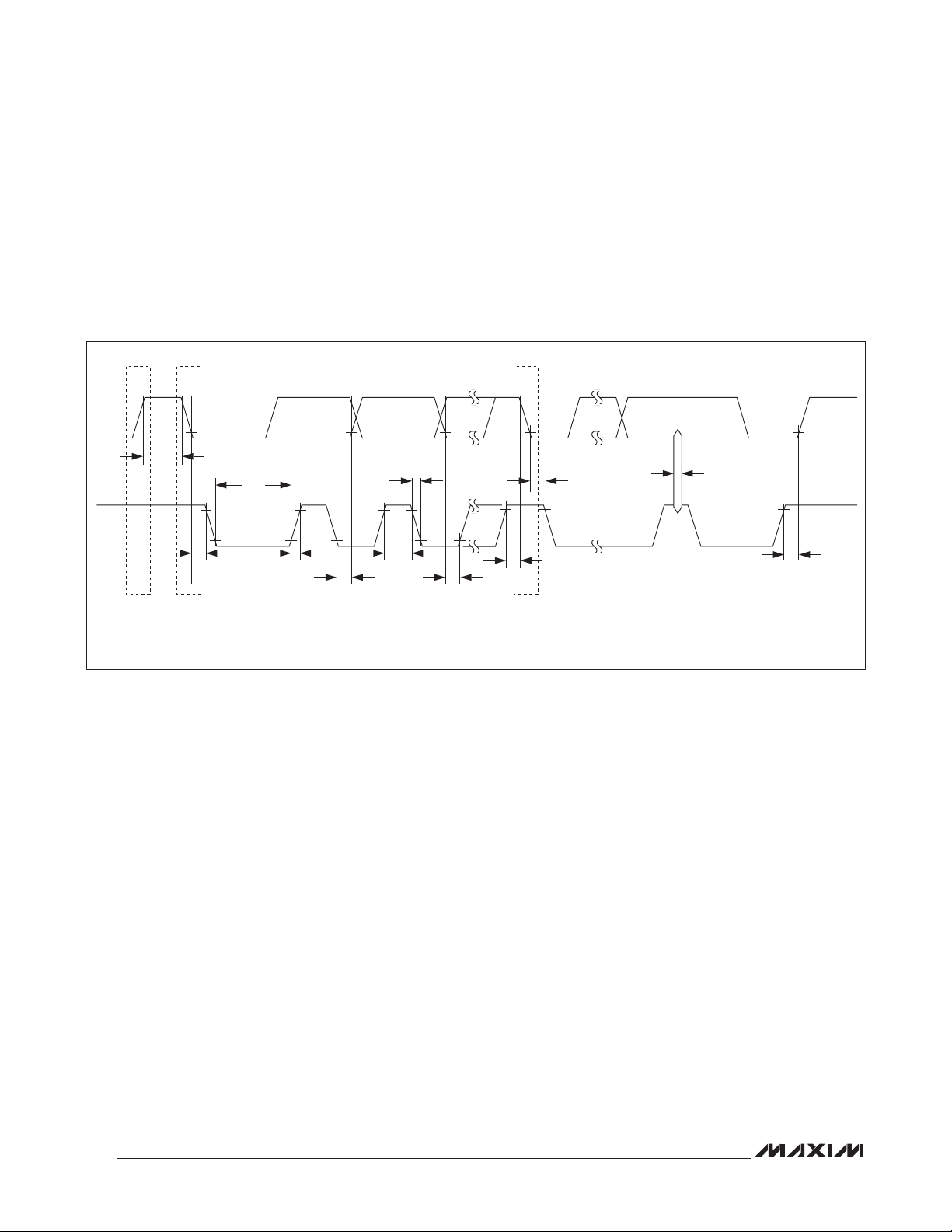
AC ELECTRICAL CHARACTERISTICS
(VCC = +1.8V to +5.5V, TA = -40NC to +85NC, unless otherwise noted.) (Note 2, Figure 1)
PARAMETER SYMBOL CONDITIONS MIN TYP MAX UNITS
SCL Clock Frequency f
Bus Free Time Between a STOP
and START Condition
Hold Time (Repeated) START
Condition
Low Period of SCL Clock t
High Period of SCL Clock t
Data Hold Time t
Data Setup Time t
Setup Time for a Repeated
START Condition
Rise Time of Both SDA and SCL
Signals
Fall Time for Both SDA and SCL
Signals
Setup Time for STOP Condition t
Capacitive Load for Each Bus
Line
I/O Capacitance C
SCL Spike Suppression t
Oscillator Stop Flag (OSF) Delay t
Timeout Interval t
t
HD:STA
HD:DAT
SU:DAT
t
SU:STA
SU:STO
TIMEOUT
SCL
t
BUF
LOW
HIGH
t
t
C
I/O
SP
OSF
(Note 6) 400 kHz
(Note 7) 0.6
(Notes 8, 9) 0 0.9
(Note 10) 100 ns
(Note 11)
R
(Note 11)
F
(Note 11) 400 pF
B
(Note 12) 25 100 ms
(Note 13) 25 35 ms
1.3
1.3
0.6
0.6
20 +
0.1C
20 +
0.1C
0.6
B
B
10 pF
30 ns
DS1341/DS1342
Fs
Fs
Fs
Fs
Fs
Fs
300 ns
300 ns
Fs
CRYSTAL PARAMETERS
PARAMETER SYMBOL CONDITIONS MIN TYP MAX UNITS
Nominal Frequency f
Series Resistance ESR 35 80
Load Capacitance C
Note 2: Limits at -40NC are guaranteed by design and not production tested.
Note 3: Voltage referenced to ground.
Note 4: Specified with I2C bus inactive. Oscillator operational, INTCN = 1, ECLK = 0.
Note 5: Applies to CLKIN/INTA and SQW/INTB only.
Note 6: The minimum SCL clock frequency is limited by the bus timeout feature, which resets the serial bus interface if SCL is
held low for t
Note 7: After this period, the first clock pulse is generated.
Note 8: A device must internally provide a hold time of at least 300ns for the SDA signal (referred to the V
nal) to bridge the undefined region of the falling edge of SCL.
Note 9: The maximum t
Note 10: A fast-mode device can be used in a standard-mode system, but the requirement t
met. This is automatically the case if the device does not stretch the low period of the SCL signal. If such a device does
stretch the low period of the SCL signal, it must output the next data bit to the SDA line t
1250ns before the SCL line is released.
TIMEOUT
.
need only be met if the device does not stretch the low period (t
HD:DAT
O
DS1341 6
L
DS1342 12.5
SU:DAT
32.768 kHz
of the SCL sig-
IHMIN
) of the SCL signal.
LOW
R to 250ns must then be
RMAX
+ t
= 1000 + 250 =
SU:DAT
kI
pF
3
Page 4
Low-Current I2C RTCs for High-ESR Crystals
Note 11: CB is the total capacitance of one bus line, including all connected devices, in pF.
Note 12: The parameter t
range of 2.4V P VCC P V
Note 13: The DS1341/DS1342 can detect any single SCL clock held low longer than t
in reset state and can receive a new START condition when SCL is held low for at least t
detects this condition, the SDA output is released. The oscillator must be running for this function to work.
SDA
t
DS1341/DS1342
SCL
NOTE: TIMING IS REFERENCED TO V
BUF
t
HD:STA
STOP START REPEATED
is the period of time the oscillator must be stopped for the OSF flag to be set over the voltage
OSF
CCMAX
.
TIMEOUTMIN
. The devices’ I2C interface is
TIMEOUTMAX
ILMAX
t
LOW
AND V
IHMIN
t
F
t
t
R
t
HD:DAT
.
HIGH
t
SU:DAT
START
t
SU:STA
t
HD:STA
t
SP
. Once the device
t
SU:STO
Figure 1. Data Transfer on I2C Serial Bus
4
Page 5
Low-Current I2C RTCs for High-ESR Crystals
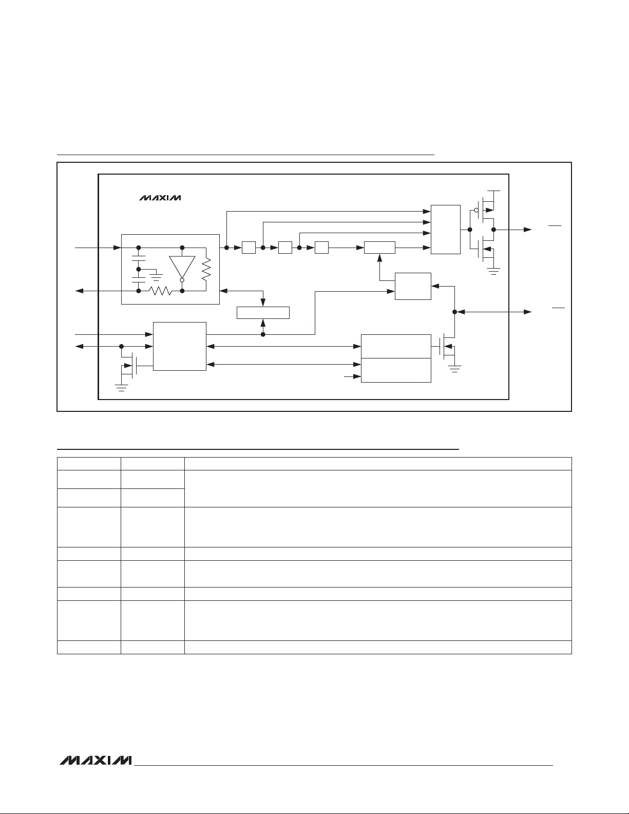
Functional Diagram
V
CC
DS1341/DS1342
32.768kHz
8.192kHz
4.096kHz
/4 /32 EXTSYNC
CONTROL LOGIC
/2
128Hz OSC-1Hz
OSC-1Hz
EXT-1Hz
ALARM AND
CONTROL REGISTERS
CLOCK AND
CALENDAR REGISTERS
DIVIDER
MUX/
BUFFER
P
SQW/INTB
N
CLKIN/INTA
N
SCL
SDA
DS1341/DS1342
X1
X2
SERIAL BUS
INTERFACE AND
ADDRESS
N
REGISTER
Pin Description
PIN NAME FUNCTION
1 X1
2 X2
3
CLKIN/INTA
4 GND Ground
5 SDA
6 SCL Serial-Clock Input. SCL is used to synchronize data movement on the serial interface.
7
8 V
SQW/INTB
CC
Connections for a Standard 32.768kHz Quartz Crystal. The internal oscillator circuitry is
designed for operation with a crystal having a specified load capacitance (CL) of 6pF (DS1341)
or 12.5pF (DS1342).
Clock Input/Active-Low Interrupt Output. This I/O pin is used to output an alarm interrupt or
accept an external clock input to drive the RTC counter. In the output mode, this is an open
drain and requires an external pullup resistor. If not used, connect this pin to ground.
Serial-Data Input/Output. SDA is the input/output pin for the I2C serial interface. The SDA pin is
open drain and requires an external pullup resistor.
Square-Wave/Active-Low Interrupt Output. This pin is used to output a programmable square
wave or an alarm interrupt signal. This is a CMOS push-pull output and does not require an
external pullup resistor. If not used, this pin can be left unconnected.
DC Power Input. This pin should be decoupled using a 0.01FF or 0.1FF capacitor.
5
Page 6

Low-Current I2C RTCs for High-ESR Crystals
Detailed Description
The DS1341/DS1342 low-current RTCs are timekeeping
devices that consume an extremely low timekeeping current, which permits longer life from a power supply. The
clock/calendar provides seconds, minutes, hours, day,
date, month, and year information. The date at the end of
the month is automatically adjusted for months with fewer
than 31 days, including corrections for leap year through
2099. The clock operates in either a 24hr or 12hr format
with an AM/PM indicator.
The DS1341/DS1342 use an external 32.768kHz crystal. The oscillator circuit does not require any external
resistors or capacitors to operate. The devices support
DS1341/DS1342
a high-ESR crystal, which broadens the pool of usable
crystals for the device. The DS1342 uses a 12.5pF crystal. The DS1341 uses a 6pF crystal, which decreases
oscillator current draw, but is less commonly available
than the 12.5pF crystals.
The DS1341/DS1342 also accept an external clock
reference for synchronization. The external clock can
be a 32.768kHz, 50Hz, 60Hz, or 1Hz source. When the
enable oscillator bit (EOSC) is a 0, the DS1341/DS1342
use the oscillator for timekeeping. If the enable external
clock input bit (ECLK) is set to 1, the time base derived
from the oscillator is compared to the 1Hz signal that is
derived from the CLKIN signal. The conditioned signal
drives the RTC time and date counters. If the oscillator
is disabled and the CLKIN signal is absent, the time and
date values remain static, provided that VCC remains at
a valid level.
When the external clock is lost or when the frequency
differs more than Q0.8% from the crystal frequency, the
signal derived from the crystal oscillator drives the RTC
counter.
When ECLK is set to 0, the RTC counter is always driven
with the signal derived from the crystal oscillator. When
the EOSC bit is a 1 and the external clock source is
selected, the RTC counter is always clocked by the signal from the CLKIN pin.
Address and data are transferred serially through an I2C
serial interface. Other features include two time-of-day
alarms, two interrupts, a programmable square-wave
output, and a bus timeout mechanism that resets the I2C
bus if it remains inactive for a minimum of t
TIMEOUT
The DS1341/DS1342 are available in a lead(Pb)-free/
RoHS-compliant, 8-pin FSOP package. Both devices
support a -40NC to +85NC extended temperature range.
Oscillator Circuit
The DS1341/DS1342 use an external 32.768kHz crystal. The oscillator circuit does not require any external
resistors or capacitors to operate. The DS1341 includes
integrated capacitive loading for a 6pF CL crystal, and
the DS1342 includes integrated capacitive loading for a
12.5pF CL crystal. See the Crystal Parameters table for
the external crystal parameters. The Functional Diagram
shows a simplified schematic of the oscillator circuit. The
startup time is usually less than 1 second when using a
crystal with the specified characteristics.
Clock Accuracy
When running from the internal oscillator, the accuracy of
the clock is dependent upon the accuracy of the crystal
and the accuracy of the match between the capacitive
load of the oscillator circuit and the capacitive load for
which the crystal was trimmed. Additional error is added
by crystal frequency drift caused by temperature shifts.
External circuit noise coupled into the oscillator circuit
can result in the clock running fast. Figure 2 shows a
typical PCB layout for isolation of the crystal and oscillator from noise. Refer to Application Note 58: Crystal
Considerations with Dallas Real-Time Clocks for detailed
information.
LOCAL GROUND PLANE (LAYER 2)
X1
CRYSTAL
X2
GND
.
NOTE: AVOID ROUTING SIGNALS IN THE CROSSHATCHED AREA (UPPER LEFT-HAND
QUADRANT) OF THE PACKAGE UNLESS THERE IS A GROUND PLANE BETWEEN THE
SIGNAL LINE AND THE PACKAGE.
Figure 2. Layout Example
6
Page 7

Low-Current I2C RTCs for High-ESR Crystals
External Synchronization
When an external clock reference is used, the input
from CLKIN/INTA is divided down to 1Hz by the divisor selected by the CLKSEL[2:1] bits. The 1Hz from the
divider (Ext-1Hz, see the Functional Diagram) is used to
correct the 1Hz that is derived from the 32.768kHz oscillator (Osc-1Hz). As Osc-1Hz drifts in relation to Ext-1Hz,
Osc-1Hz is digitally adjusted.
As shown in the Functional Diagram, the three highest frequencies driving the SQW/INTB pin are derived
from the uncorrected oscillator, while the 1Hz output is
derived from the adjusted Osc-1Hz signal.
Conceptually, the circuit can be thought of as two 1Hz
signals, one derived from the internal oscillator and the
other derived from the external reference clock, with the
oscillator-derived 1Hz signal being locked to the 1Hz
signal derived from the external reference clock. The
edges of the 1Hz signals do not need to be aligned with
OSC-1Hz
FROM OSCILLATOR
each other. While the external clock source is present
DS1341/DS1342
and within tolerance, the Ext-1Hz and Osc-1Hz maintain
their existing lock, regardless of their edge alignment,
with periodic correction of the Osc-1Hz signal. If the
external signal is lost and then regained sometime later,
the signals relock with whatever new alignment exists
(see Figure 3).
The Ext-1Hz is used by the device as long as it is within
tolerance, which is about 0.8% of Osc-1Hz. While Ext1Hz is within tolerance, the skew between the two signals could shift until a change of approximately 7.8ms
accumulates, after which the Osc-1Hz signal is adjusted
(see Figure 4). The adjustment is accomplished by digitally adjusting the 32kHz oscillator divider chain.
If the difference between Ext-1Hz and Osc-1Hz is greater
than approximately 0.8%, Osc-1Hz runs unadjusted (see
Figure 3) and the loss of signal (LOS) is set, provided the
ECLK bit is set.
SKEW SKEW
FROM EXTERNAL REFERENCE
Figure 3. Loss and Reacquisition of External Reference Clock
FROM EXTERNAL REFERENCE
EXT-1Hz
BREAK IN EXTERNAL REFERENCE SIGNAL
OSC-1Hz
FROM OSCILLATOR
CURRENT LOCK SHIFTED BACK TO CURRENT LOCKDRIFT AFTER N CYCLES
EXT-1Hz
Figure 4. Drift and Adjustment of Internal 1Hz to External Reference Clock
7
Page 8
Low-Current I2C RTCs for High-ESR Crystals
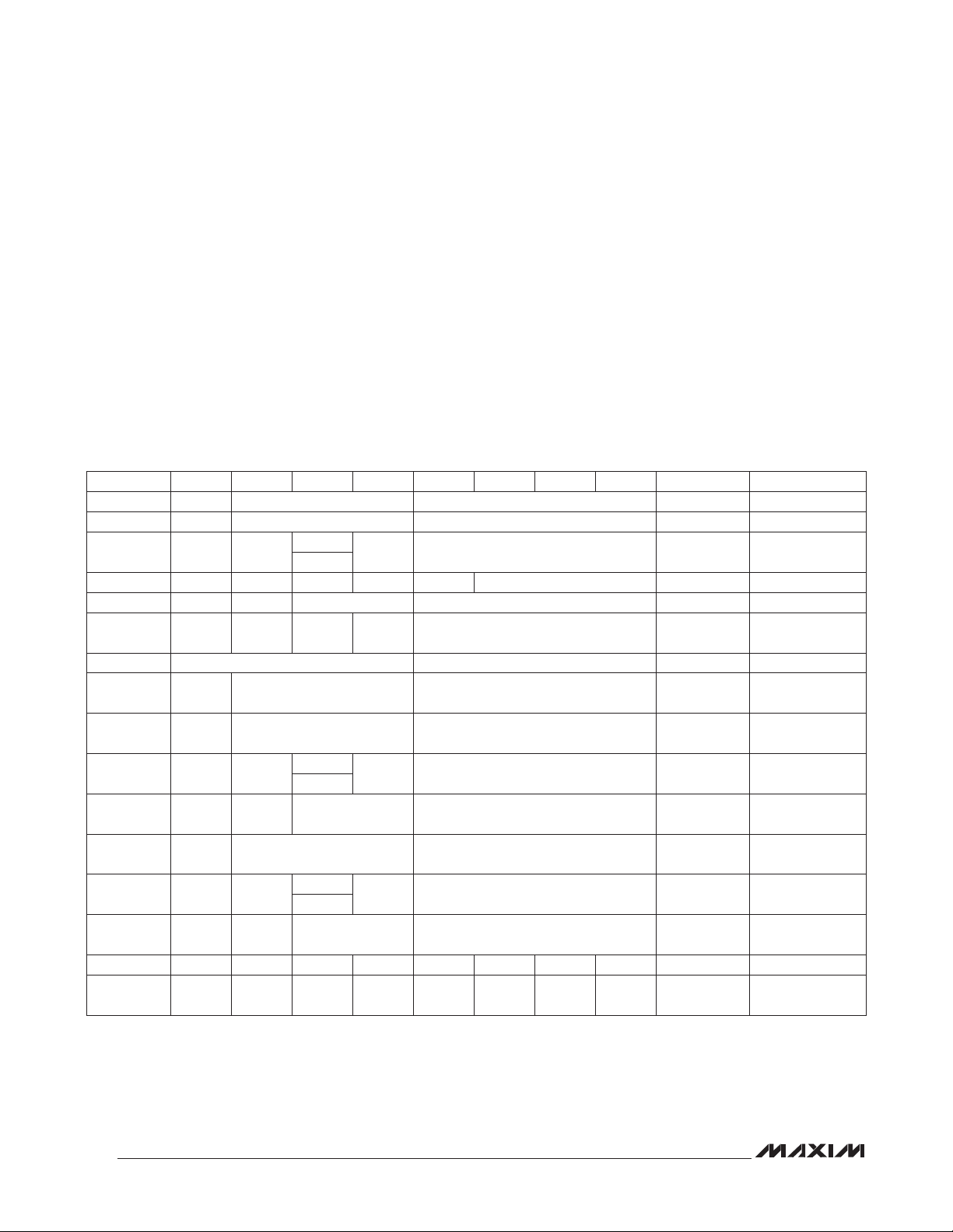
Register Map
Table 1 shows the map for the DS1341/DS1342 registers. During a multibyte access, if the address pointer
reaches the end of the register space (0Fh), it wraps
around to location 00h. On either an I2C START or
address pointer incrementing to location 00h, the current
time is transferred to a second set of registers. The time
information is read from these secondary registers while
the clock continues to run. This eliminates the need to
reread the registers in case the main registers update
during a read.
Table 1. Register Map
DS1341/DS1342
ADDRESS BIT 7 BIT 6 BIT 5 BIT 4 BIT 3 BIT 2 BIT 1 BIT 0 FUNCTION RANGE
00h 0 10 Seconds Seconds Seconds 00–59
01h 0 10 Minutes Minutes Minutes 00–59
02h 0
03h 0 0 0 0 0 Day Day 1–7
04h 0 0 10 Date Date Date 01–31
05h CENT 0 0 10 MO Month
06h 10 Year Year Year 00–99
07h A1M1 10 Seconds Seconds
08h A1M2 10 Minutes Minutes
09h A1M3
0Ah A1M4
0Bh A2M2 10 Minutes Minutes
0Ch A2M3
0Dh A2M4
0Eh
0Fh OSF DOSF LOS CLKSEL2 CLKSEL1 ECLK A2F A1F
Note: Bits listed as 0 always read back as 0 and cannot be written to a 1.
EOSC
12/24
12/24
DY/DT
12/24
DY/DT
AM/PM
10hr
AM/PM
10hr
AM/PM
10hr
0 EGFIL RS2 RS1 INTCN A2IE A1IE Control —
10hr Hour Hours
10hr Hour
10 Date
10hr Hour
10 Date
The I2C interface is guaranteed to operate when VCC is
between 1.8V and 5.5V and the EOSC bit is 0. The I2C
interface is accessible whenever VCC is at a valid level.
To prevent invalid device operation, the I2C interface
should not be accessed when VCC is below +1.8V.
If a microcontroller connected to the DS1341/DS1342
resets during I2C communications, it is possible that the
microcontroller and the DS1341/DS1342 could become
unsynchronized. When the microcontroller resets, the
DS1341/DS1342 I2C interface can be placed into a
Month/
Century
Alarm 1
Seconds
Alarm 1
Minutes
Alarm 1
Hours
Day,
Date
Day,
Date
Alarm 1 Day,
Alarm 1 Date
Alarm 2
Minutes
Alarm 2
Hours
Alarm 2 Day,
Alarm 2 Date
Control/
Status
I2C Interface
1–12+AM/PM
01–12 + Century
1–12 + AM/PM
1–12 + AM/PM
00–23
00–59
00–59
00–23
1–7
1–31
00–59
00–23
1–7
1–31
—
8
Page 9

Low-Current I2C RTCs for High-ESR Crystals
known state by holding SCL low for t
limits the minimum frequency at which the I2C interface
can be operated. If data is being written to the device
when the interface timeout is exceeded, prior to the
acknowledge, the incomplete byte of data is not written.
TIMEOUT
. Doing so
Clock and Calendar (00h–06h)
The time and calendar information is obtained by reading the appropriate register bytes. The RTC registers are
illustrated in Table 1. The time and calendar are set or
initialized by writing the appropriate register bytes. The
contents of the time and calendar registers are in the
binary-coded decimal (BCD) format. The Day register
increments at midnight and rolls over from 7 to 1. Values
that correspond to the day-of-week are user-defined
but must be sequential (i.e., if 1 equals Sunday, then 2
equals Monday, and so on). The CENT bit in the Month
register toggles when the Years register rolls over from
99 to 00. Illogical time and date entries result in an undefined operation.
The DS1341/DS1342 can be run in either 12hr or 24hr
mode. Bit 6 of the Hours register is defined as the 12hr
or 24hr mode select bit. When high, the 12hr mode is
selected. In the 12hr mode, bit 5 is the AM/PM bit, with
a content of 1 being PM. In the 24hr mode, bit 5 is the
second bit of the 10hr field. The century bit (bit 7 of the
DS1341/DS1342
Month register) is toggled when the Years register increments from 99 to 00. On a power-on reset (POR), the
time and date are set to 00:00:00 00/01/01 and the Day
register is set to 01.
Alarms (07h–0Dh)
The DS1341/DS1342 contain two time-of-day/date
alarms. Alarm 1 can be set by writing to registers 07h–
0Ah. Alarm 2 can be set by writing to registers 0Bh–0Dh.
The alarms can be programmed to activate the CLKIN/
INTA or SQW/INTB outputs (see Table 5) on an alarm
match condition. Bit 7 of each of the time of day/date
alarm registers are mask bits. When all the mask bits for
each alarm are 0, an alarm only occurs when the values
in the timekeeping registers 00h–06h match the values
stored in the time of day/date alarm registers. The alarms
can also be programmed to repeat every second, minute, hour, day, or date. Tables 2 and 3 show the possible
alarm settings. Configurations not listed in the tables
result in illogical operation. POR values are undefined.
The DY/DT bits (bit 6 of the alarm day/date registers)
control whether the alarm value stored in bits 0 to 5 of
that register reflects the day of the week or the date of
the month. If DY/DT is written to 0, the alarm is the result
Table 2. Alarm 1 Mask Bits
DY/DT
X 1 1 1 1 Alarm once per second.
X 1 1 1 0 Alarm when seconds match.
X 1 1 0 0 Alarm when minutes and seconds match.
X 1 0 0 0 Alarm when hours, minutes, and seconds match.
0 0 0 0 0 Alarm when date, hours, minutes, and seconds match.
1 0 0 0 0 Alarm when day, hours, minutes, and seconds match.
X = Don’t care.
ALARM 1 MASK BITS (BIT 7)
A1M4 A1M3 A1M2 A1M1
ALARM RATE
Table 3. Alarm 2 Mask Bits
DY/DT
X 1 1 1 Alarm once per minute (00 second of every minute).
X 1 1 0 Alarm when minutes match.
X 1 0 0 Alarm when hours and minutes match.
0 0 0 0 Alarm when date, hours, and minutes match.
1 0 0 0 Alarm when day, hours, and minutes match.
X = Don’t care.
ALARM 2 MASK BITS (BIT 7)
A2M4 A2M3 A2M2
ALARM RATE
9
Page 10
Low-Current I2C RTCs for High-ESR Crystals
of a match with date of the month. If DY/DT is written to
1, the alarm is the result of a match with day of the week.
When the RTC register values match alarm register settings, the corresponding alarm flag bit (A1F or A2F) is
set to 1 in the Control/Status register. If the corresponding alarm interrupt enable bit (A1IE or A2IE) is also set
to 1 in the Control register, the alarm condition activates
the output(s) defined by the ECLK and INTCN bits (see
Table 5).
Control Register (0Eh)
Bit 7: Enable Oscillator (EOSC). When the EOSC bit
is 0, the oscillator is enabled. When this bit is a 1, the
oscillator is disabled. This bit is cleared (0) when power
DS1341/DS1342
is first applied.
Bit 6: No Function
Bit 5: Enable Glitch Filter (EGFIL). When the EGFIL bit
is 1, the 5Fs glitch filter at the output of the crystal oscillator is enabled. The glitch filter is disabled when this bit
is 0. Disabling the glitch filter is useful in reducing power
consumption. This bit is cleared (0) when power is first
applied.
Bits 4 and 3: Rate Select (RS[2:1]). These bits control the frequency of the square-wave output when the
square wave has been enabled. Table 4 shows the
square-wave frequencies that can be selected with the
RS bits. These bits are both set to 1 (32.768kHz) when
power is first applied.
The 32.768kHz oscillator is the source of all square-wave
output frequencies. Frequencies above 1Hz are not conditioned by CLKIN. The 1Hz output is the 32.768kHz oscillator frequency, divided down to 1Hz and conditioned by
CLKIN, provided that the CLKIN frequency differs by no
more than Q0.8% from the crystal frequency. Cycle-tocycle jitter of the 1Hz square wave can be up to 2ms.
Bit 2: Interrupt Control (INTCN). This bit controls the
relationship between the two alarms and the interrupt
output pins. When the INTCN bit is 0, a square wave is
output on the SQW/INTB pin, and the state of the ECLK
bit determines the function of the CLKIN/INTA pin (see
Table 5). When the INTCN bit is 1 and the ECLK bit is a
0, a match between the timekeeping registers and the
alarm 1 registers activates the CLKIN/INTA pin (provided
that the alarm is enabled) and a match between the
timekeeping registers and the alarm 2 registers activates
the SQW/INTB pin (provided that the alarm is enabled).
When the INTCN bit is 1 and the ECLK bit is a 1, a match
between the timekeeping registers and the alarm 1
registers or a match between the timekeeping registers
and the alarm 2 registers activates the SQW/INTB pin
(provided that the alarm is enabled). This bit is cleared
(0) when power is first applied.
Bit 1: Alarm 2 Interrupt Enable (A2IE). When the A2IE
bit is 0, the alarm 2 interrupt function is disabled. When
the A2IE bit is 1, the alarm 2 interrupt function is enabled
and is routed to an output, based upon the steering
defined by the INTCN and ECLK bits, as noted in Table
5. Regardless of the state of A2IE, a match between
the timekeeping registers and the alarm 2 registers
(0Bh–0Dh) sets the alarm 2 flag bit (A2F). This bit is
cleared (0) when power is first applied.
Bit 0: Alarm 1 Interrupt Enable (A1IE). When the A1IE
bit is 0, the alarm 1 interrupt function is disabled. When
the A1IE bit is 1, the alarm 1 interrupt function is enabled
and is routed to an output, based upon the steering
defined by the INTCN and ECLK bits, as noted in Table
5. Regardless of the state of A1IE, a match between the
timekeeping registers and the alarm 1 registers (07h–
0Ah) sets the alarm 1 flag bit (A1F). This bit is cleared (0)
when power is first applied.
Control Register Bitmap (0Eh)
BIT 7
EOSC
0 0 0 1 1 0 0 0
BIT 6 BIT 5 BIT 4 BIT 3 BIT 2 BIT 1 BIT 0
0 EGFIL RS2 RS1 INTCN A2IE A1IE
Table 4. SQW/INTB Output Settings Table 5. Interrupt Output Routing
RS2 RS1
0 0 1Hz
0 1 4.098kHz
1 0 8.192kHz
1 1 32.768kHz
10
SQW/INTB
INTCN ECLK
0 0 A1F + A2F SQW
0 1 CLKIN Input SQW
1 0 A1F A2F
1 1 CLKIN Input A1F + A2F
CLKIN/INTA SQW/INTB
Page 11

Low-Current I2C RTCs for High-ESR Crystals
Control/Status Register Bitmap (0Fh)
BIT 7 BIT 6 BIT 5 BIT 4 BIT 3 BIT 2 BIT 1 BIT 0
OSF DOSF LOS CLKSEL2 CLKSEL1 ECLK A2F A1F
1 0 1 0 0 0 X X
Control/Status Register (0Fh)
Bit 7: Oscillator Stop Flag (OSF). If the OSF bit is a 1,
that indicates the oscillator has stopped or was stopped
for some period of time, and could be used to judge
the validity of the clock and calendar data. This bit is
edge triggered and is set to 1 when the internal circuitry
senses the oscillator has transitioned from a normal run
state to a STOP condition. The following are examples of
conditions that can cause the OSF bit to be set:
1) Power is applied for the first time.
2) The voltage present on VCC is insufficient to support
oscillation.
3) The EOSC bit is turned off.
4) There are external influences on the crystal (e.g.,
noise, leakage, etc.).
This bit remains at 1 until written to 0. Attempting to write
OSF to 1 leaves the value unchanged.
Bit 6: Disable Oscillator Stop Flag (DOSF). This bit,
when set to 1, disables the sensing of the oscillator
conditions that would set the OSF bit. OSF remains
at 0 regardless of what happens to the oscillator.
This bit is cleared (0) when power is first applied.
Disabling the oscillator sensing is useful in reducing
power consumption.
Bit 5: Loss of Signal (LOS). This status bit indicates the
state of the CLKIN pin. The bit is set to 1 when the RTC
counter is no longer conditioned by the external clock.
This happens when ECLK = 0, or when the clock signal
at CLKIN stops toggling, or when the CLKIN frequency
differs more than Q0.8% from the selected input frequency. This bit remains at 1 until written to 0. Attempting
to write LOS to 1 leaves the value unchanged. Clearing
the LOS flag when the CLKIN frequency is invalid inhibits
subsequent detections of the input frequency deviation.
Bits 4 and 3: Select Clock Source (CLKSEL[2:1]).
These two register bits select the clock source to drive
the RTC counter. Table 6 lists the input frequencies that
can be selected. Upon power-up, the bits are cleared to
0 and the 1Hz rate is selected.
Table 6. Input Frequency Options
CLKSEL2 CLKSEL1
0 0 1Hz Input
0 1 50Hz Input
1 0 60Hz Input
1 1 32.768kHz Input
Bit 2: Enable External Clock Input (ECLK). This bit
controls the direction of the CLKIN/INTA pin (see Table
5). When the ECLK bit is 1, the CLKIN/INTA pin is an
input, with the expected input rate defined by the state
of CLKSEL2 and CLKSEL1 (see Table 6).
When the ECLK bit is 0, the CLKIN/INTA pin is an
interrupt output (see Table 5). If the INTCN bit is 0,
CLKIN/INTA contains the status of A1F (provided that
the A1IE bit is 1) or A2F (provided that the A2IE bit is 1).
If the INTCN bit is 1, CLKIN/INTA contains the status of
A1F (provided that the A1IE bit is 1).
This bit is set to 0 when power is first applied.
Bit 1: Alarm 2 Flag (A2F). A 1 in the alarm 2 flag bit
indicates that the time matched the alarm 2 registers.
This flag can be used to generate an interrupt on either
CLKIN/INTA or SQW/INTB depending on the status of
the INTCN bit in the Control register. If the INTCN bit is
set to 0 and A2F bit is a 1 (and A2IE bit is also 1), the
CLKIN/INTA pin goes low. If the INTCN bit is set to 1 and
A2F bit is 1 (and A2IE bit is also 1), the SQW/INTB pin
goes low. The A2F bit is cleared when written to 0. This
bit can only be written to 0. Attempting to write this bit to
1 leaves the value unchanged.
Bit 0: Alarm 1 Flag (A1F). A 1 in the alarm 1 flag bit
indicates that the time matched the alarm 1 registers. If
the A1IE bit is also 1, the CLKIN/INTA pin goes low. A1F
is cleared when written to 0. This bit can only be written
to 0. Attempting to write this bit to 1 leaves the value
unchanged.
DS1341/DS1342
CLKIN/INTA
11
Page 12

Low-Current I2C RTCs for High-ESR Crystals
I2C Serial Port Operation
I2C Slave Address
The DS1341/DS1342s’ slave address byte is D0h. The
first byte sent to the device includes the device identifier,
device address, and the R/W bit (Figure 5). The device
address sent by the I2C master must match the address
assigned to the device.
I2C Definitions
The following terminology is commonly used to describe
I2C data transfers.
Master Device: The master device controls the slave
devices on the bus. The master device generates
DS1341/DS1342
SCL clock pulses and START and STOP conditions.
Slave Devices: Slave devices send and receive data
at the master’s request.
Bus Idle or Not Busy: Time between STOP and
START conditions when both SDA and SCL are
inactive and in their logic-high states. When the bus
is idle, it often initiates a low-power mode for slave
devices.
START Condition: A START condition is generated
by the master to initiate a new data transfer with a
slave. Transitioning SDA from high to low while SCL
remains high generates a START condition. See
Figure 1 for applicable timing.
STOP Condition: A STOP condition is generated
by the master to end a data transfer with a slave.
Transitioning SDA from low to high while SCL remains
high generates a STOP condition. See Figure 1 for
applicable timing.
Repeated START Condition: The master can use
a repeated START condition at the end of one data
transfer to indicate that it immediately initiates a new
data transfer following the current one. Repeated
STARTs are commonly used during read operations
to identify a specific memory address to begin a data
transfer. A repeated START condition is issued identically to a normal START condition. See Figure 1 for
applicable timing.
MSB
1 1 10 R/W000
DEVICE
IDENTIFIER
Figure 5. Slave Address Byte
DEVICE
ADDRESS
LSB
READ/
WRITE BIT
Bit Write: Transitions of SDA must occur during
the low state of SCL. The data on SDA must remain
valid and unchanged during the entire high pulse of
SCL plus the setup and hold time requirements (see
Figure 1). Data is shifted into the device during the
rising edge of the SCL.
Bit Read: At the end of a write operation, the master
must release the SDA bus line for the proper amount
of setup time (see Figure 1) before the next rising
edge of SCL during a bit read. The device shifts out
each bit of data on SDA at the falling edge of the
previous SCL pulse and the data bit is valid at the
rising edge of the current SCL pulse. Remember that
the master generates all SCL clock pulses including
when it is reading bits from the slave.
Acknowledge (ACK and NACK): An acknowledge
(ACK) or not acknowledge (NACK) is always the
ninth bit transmitted during a byte transfer. The
device receiving data (the master during a read or
the slave during a write operation) performs an ACK
by transmitting a 0 during the ninth bit. A device performs a NACK by transmitting a 1 during the ninth bit.
Timing for the ACK and NACK is identical to all other
bit writes. An ACK is the acknowledgment that the
device is properly receiving data. A NACK is used to
terminate a read sequence or as an indication that the
device is not receiving data.
Byte Write: A byte write consists of 8 bits of information transferred from the master to the slave (most
significant bit first) plus a 1-bit acknowledgment from
the slave to the master. The 8 bits transmitted by the
master are done according to the bit write definition
and the acknowledgment is read using the bit read
definition.
Byte Read: A byte read is an 8-bit information transfer
from the slave to the master plus a 1-bit ACK or NACK
from the master to the slave. The 8 bits of information
that are transferred (most significant bit first) from the
slave to the master are read by the master using the
bit read definition, and the master transmits an ACK
using the bit write definition to receive additional data
bytes. The master must NACK the last byte read to
terminate communication so the slave returns control
of SDA to the master.
Slave Address Byte: Each slave on the I2C bus
responds to a slave address byte sent immediately
following a START condition. The slave address byte
contains the slave address in the most significant 7
bits and the R/W bit in the least significant bit. The
12
Page 13
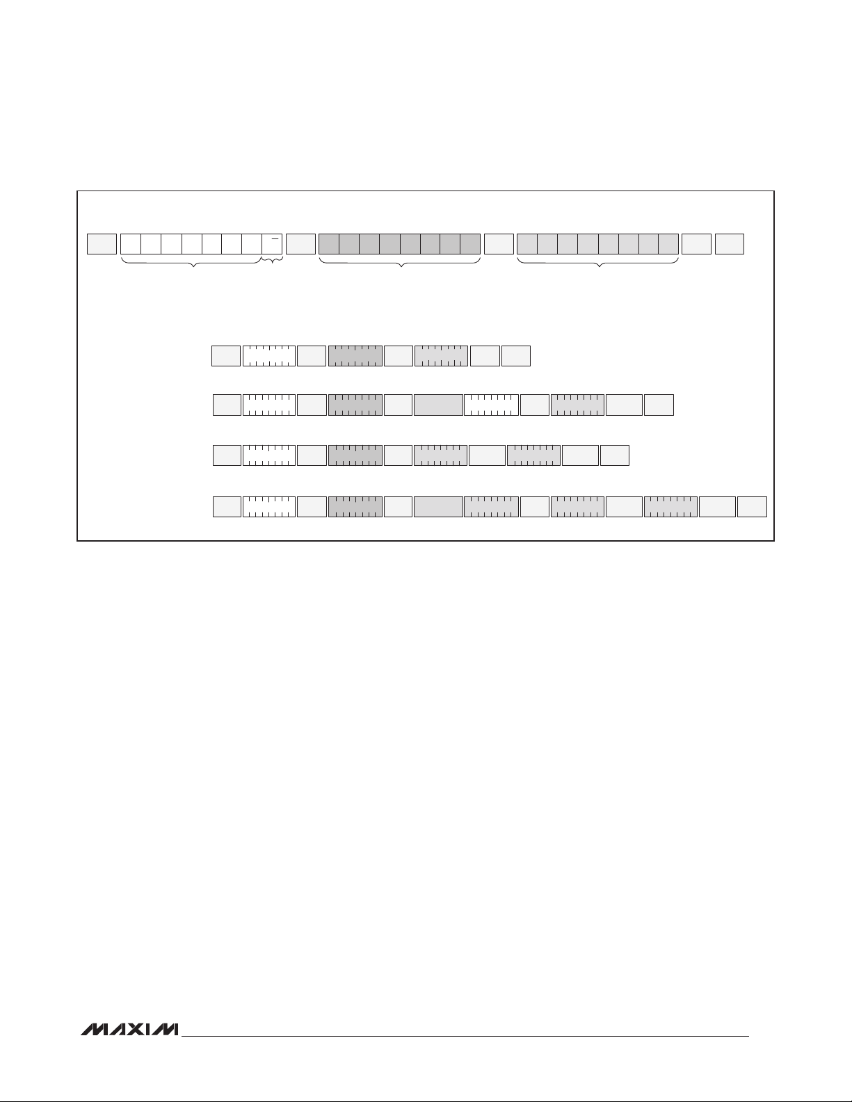
Low-Current I2C RTCs for High-ESR Crystals
2
C WRITE TRANSACTION
TYPICAL I
MSB LSB MSB LSB MSB LSB
START
1 1 0 1 0 0 0
R/W
SLAVE
b7 b6 b5 b4 b3 b2 b1 b0
ACK
SLAVE
b7 b6 b5 b4 b3 b2 b1 b0
ACK
SLAVE
ACK
DS1341/DS1342
STOP
READ/
WRITE
D0h 0Eh
1 1 0 1 0 0 0 0 0 0 0 0 1 1 1 0
SLAVE
ACK
D0h
SLAVE
ACK
D0h 04h
SLAVE
ACK
D0h 0Ch
SLAVE
ACK
0Eh
2
EXAMPLE I
C TRANSACTIONS
A)
SINGLE BYTE WRITE
-WRITE CONTROL REGISTER
TO 18h
B)
SINGLE BYTE READ
-READ CONTROL REGISTER
C)
MULTIBYTE WRITE
-WRITE DATE REGISTER
TO "02" AND MONTH
REGISTER TO "11"
D)
MULTIBYTE READ
-READ ALARM 2 HOURS
AND DATE VALUES
SLAVE
ADDRESS
START
START
START 1 1 0 1 0 0 0 0 0 0 0 0 0 1 0 0
START 1 1 0 1 0 0 0 0 0 0 0 0 1 1 0 0
Figure 6. I2C Transactions
DS1341/DS1342s’ slave address is D0h and cannot
be modified by the user. When the R/W bit is 0 (such
as in D0h), the master is indicating it writes data to the
slave. If R/W = 1 (D1h in this case), the master is indicating it wants to read from the slave. If an incorrect
slave address is written, the DS1341/DS1342 assume
the master is communicating with another I2C device
and ignore the communication until the next START
condition is sent.
Memory Address: During an I2C write operation, the
master must transmit a memory address to identify
the memory location where the slave is to store the
data. The memory address is always the second byte
transmitted during a write operation following the
slave address byte.
I2C Communication
See Figure 6 for an I2C communication example.
Writing a Single Byte to a Slave: The master must
generate a START condition, write the slave address
byte (R/W = 0), write the memory address, write
the byte of data, and generate a STOP condition.
Remember the master must read the slave’s acknowledgment during all byte write operations.
REGISTER ADDRESS
SLAVE
0 0 0 1 1 0 0 0
ACK
SLAVE
ACK
SLAVE
0 0 0 0 0 0 1 0
ACK
SLAVE
ACK
DATA
18h
SLAVE
STOP
ACK
REPEATED
START
02h
REPEATED
START
D1h
D1h
SLAVE
ACK
11h
0 0 0 1 0 0 0 1
SLAVE
ACK
1 1 0 1 0 0 0 1
SLAVE
ACK
1 1 0 1 0 0 0 1 VALUE
DATA
VALUE
SLAVE
ACK
DATA
MASTER
NACK
STOP
MASTER
STOP1 1 0 1 0 0 0 0 0 0 0 0 1 1 1 0
DATA
ACK
Writing Multiple Bytes to a Slave: To write multiple
bytes to a slave, the master generates a START condition, writes the slave address byte (R/W = 0), writes
the starting memory address, writes multiple data
bytes, and generates a STOP condition.
Reading a Single Byte from a Slave: Unlike the write
operation that uses the specified memory address
byte to define where the data is to be written, the read
operation occurs at the present value of the memory
address counter. To read a single byte from the slave,
the master generates a START condition, writes the
slave address byte with R/W = 1, reads the data byte
with a NACK to indicate the end of the transfer, and
generates a STOP condition. However, since requiring the master to keep track of the memory address
counter is impractical, use the method for manipulating the address counter for reads.
Manipulating the Address Counter for Reads: A
dummy write cycle can be used to force the address
counter to a particular value. To do this the master generates a START condition, writes the slave
address byte (R/W = 0), writes the memory address
where it desires to read, generates a repeated START
condition, writes the slave address byte (R/W = 1),
MASTER
NACK
STOPVALUE
13
Page 14

Low-Current I2C RTCs for High-ESR Crystals
reads data with ACK or NACK as applicable, and
generates a STOP condition. See Figure 6 for a read
example using the repeated START condition to
specify the starting memory location.
Reading Multiple Bytes from a Slave: The read
operation can be used to read multiple bytes with a
single transfer. When reading bytes from the slave,
the master simply ACKs the data byte if it desires to
read another byte before terminating the transaction.
After the master reads the last byte it must NACK to
indicate the end of the transfer and then it generates
a STOP condition.
Bus Timeout
DS1341/DS1342
To avoid an unintended I2C interface timeout, SCL
should not be held low longer than t
I2C interface is in the reset state and can receive a
new START condition when SCL is held low for at least
t
TIMEOUTMAX
SDA is released and allowed to be pulled high by the
external pullup resistor. For the timeout function to work,
the oscillator must be enabled and running.
. When the device detects this condition,
TIMEOUTMIN
. The
Applications Information
Power-Supply Decoupling
To achieve the best results when using the DS1341/
DS1342, decouple the VCC power supply with a 0.01FF
and/or 0.1FF capacitor. Use a high-quality, ceramic, surface-mount capacitor if possible. Surface-mount compo-
nents minimize lead inductance, which improves performance, and ceramic capacitors tend to have adequate
high-frequency response for decoupling applications.
Using Open-Drain Outputs
The CLKIN/INTA output is open drain and, therefore,
requires an external pullup resistor to realize a logic-high
output level.
SDA and SCL Pullup Resistors
SDA is an open-drain output and requires an external
pullup resistor to realize a logic-high level.
Because the DS1341/DS1342 do not use clock cycle
stretching, a master using either an open-drain output
with a pullup resistor or CMOS output driver (push-pull)
could be used for SCL.
Chip Information
SUBSTRATE CONNECTED TO GROUND
Package Information
For the latest package outline information and land patterns, go to www.maxim-ic.com/packages. Note that
a “+”, “#”, or “-” in the package code indicates RoHS
status only. Package drawings may show a different suffix character, but the drawing pertains to the package
regardless of RoHS status.
PACKAGE TYPE PACKAGE CODE DOCUMENT NO.
8 FSOP
U8+1
21-0036
Maxim cannot assume responsibility for use of any circuitry other than circuitry entirely embodied in a Maxim product. No circuit patent licenses are implied.
Maxim reserves the right to change the circuitry and specifications without notice at any time.
14 Maxim Integrated Products, 120 San Gabriel Drive, Sunnyvale, CA 94086 408-737-7600
©
2009 Maxim Integrated Products Maxim is a registered trademark of Maxim Integrated Products, Inc.
 Loading...