

Page 1
DS1315
PRELIMINARY
DS1315
Phantom Time Chip
FEATURES
• Real time clock keeps track of hundredths of seconds,
seconds, minutes, hours, days, date of the month,
months, and years
• Adjusts for months with fewer than 31 days
• Automatic leap year correction valid up to 2100
• No address space required to communicate with RTC
• Provides nonvolatile controller functions for battery
backup of SRAM
• Supports redundant battery attachment for high–reli-
ability applications
• Full ±10% V
operating range
CC
• +3.3 volt or +5 volt operation
• Industrial (–45°C to +85°C) operating temperature
ranges available
• Drop in replacement for DS1215
ORDERING INFORMATION
DS1315XX–XX
33–3.3 volt operation
5–5 volt operation
blank–commercial temp range
N–industrial temp range
blank–16–pin DIP
S–16–pin SOIC
E–20–pin TSSOP
PIN ASSIGNMENT
X1
X2
WE
BAT1
GND
D
Q
GND
16–PIN DIP (300 MIL)
X1
X2
WE
BAT1
GND
D
Q
GND
16–PIN SOIC (300 MIL)
X1
X2
WE
NC
BAT1
GND
NC
D
Q
GND
1
16
2
15
3
14
4
13
5
12
6
11
7
10
8
1
2
3
4
5
6
7
8
16
15
14
13
12
11
10
1
2
3
4
5
6
7
8
9
10
20–PIN TSSOP
9
20
19
18
17
16
15
14
13
12
11
9
V
CCI
V
CCO
BAT2
RST
OE
CEI
CEO
ROM/RAM
V
CCI
V
CCO
BAT2
RST
OE
CEI
CEO
ROM/RAM
V
CCI
V
CCO
BAT2
NC
RST
OE
NC
CEI
CEO
ROM/RAM
Copyright 1995 by Dallas Semiconductor Corporation.
All Rights Reserved. For important information regarding
patents and other intellectual property rights, please refer to
Dallas Semiconductor data books.
041697 1/22
Page 2
DS1315
PIN DESCRIPTION
X1, X2 – 32.768 KHz Crystal Connection
WE – Write Enable
BAT1 – Battery 1 Input
GND – Ground
D – Data Input
Q – Data Output
ROM/RAM
– ROM/RAM Mode Select
CEO – Chip Enable Output
CEI – Chip Enable Input
OE
– Output Enable
RST – Reset
BAT2 – Battery 2 Input
V
V
CCO
CCI
– Switched Supply Output
– Power Supply Input
DESCRIPTION
The DS1315 Phantom Time Chip is a combination of a
CMOS timekeeper and a nonvolatile memory controller.
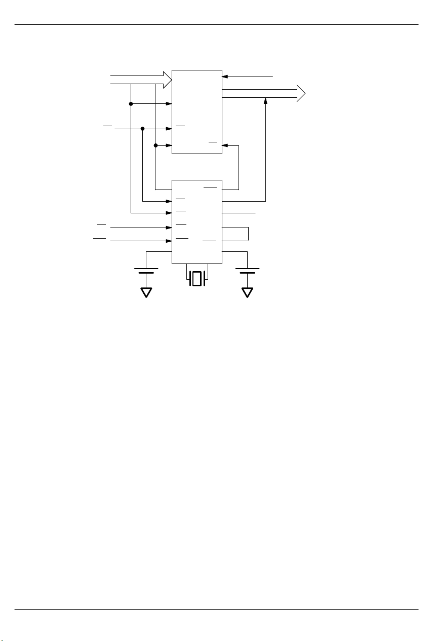
TIMING BLOCK DIAGRAM Figure 1
32.768 KHz
ROM/RAM
CEO
CEI
OE
WE
RST
CONTROL
LOGIC
POWER–FAIL
READ
WRITE
X
1
X
2
In the absence of power, an external battery maintains
the timekeeping operation and provides power for a
CMOS static RAM. The watch keeps track of hundredths of seconds, seconds, minutes, hours, day, date,
month, and year information. The last day of the month
is automatically adjusted for months with less than
31 days, including leap year correction. The watch operates in one of two formats: a 12–hour mode with an
AM/PM indicator or a 24–hour mode. The nonvolatile
controller supplies all the necessary support circuitry to
convert a CMOS RAM to a nonvolatile memory. The
DS1315 can be interfaced with either RAM or ROM
without leaving gaps in memory .
OPERATION
The block diagram of Figure 1 illustrates the main elements of the Time Chip. The following paragraphs
describe the signals and functions.
CLOCK/CALENDAR LOGIC
UPDATE
TIMEKEEPING REGISTER
041697 2/22
ACCESS
ENABLE
SEQUENCE
DETECTOR
D
Q
I/O BUFFERS
V
CCI
DATA
POWER–FAIL
DETECT
LOGIC
BAT
1
BAT
INTERNAL V
2
COMPARISON REGISTER
CC
V
CCO
Page 3

DS1315
Communication with the Time Chip is established by
pattern recognition of a serial bit stream of 64 bits which
must be matched by executing 64 consecutive write
cycles containing the proper data on data in (D). All
accesses which occur prior to recognition of the 64–bit
pattern are directed to memory via the chip enable output pin (CEO
).
After recognition is established, the next 64 read or write
cycles either extract or update data in the Time Chip and
CEO
remains high during this time, disabling the con-
nected memory.
Data transfer to and from the timekeeping function is
accomplished with a serial bit stream under control of
chip enable input (CEI
), output enable (OE), and write
enable (WE). Initially , a read cycle using the CEI and OE
control of the Time Chip starts the pattern recognition
sequence by moving pointer to the first bit of the 64–bit
comparison register. Next, 64 consecutive write cycles
are executed using the CEI
and WE control of the Time
Chip. These 64 write cycles are used only to gain
access to the Time Chip.
When the first write cycle is executed, it is compared to
bit 1 of the 64–bit comparison register. If a match is
found, the pointer increments to the next location of the
comparison register and awaits the next write cycle. If a
match is not found, the pointer does not advance and all
subsequent write cycles are ignored. If a read cycle occurs at any time during pattern recognition, the present
sequence is aborted and the comparison register pointer is reset. Pattern recognition continues for a total of 64
write cycles as described above until all the bits in the
comparison register have been matched. (This bit pattern is shown in Figure 2). With a correct match for
64 bits, the Time Chip is enabled and data transfer to or
from the timekeeping registers may proceed. The next
64 cycles will cause the Time Chip to either receive data
on D, or transmit data on Q, depending on the level of
OE
pin or the WE pin. Cycles to other locations outside
the memory block can be interleaved with CEI
cycles
without interrupting the pattern recognition sequence or
data transfer sequence to the Time Chip.
A standard 32,768 KHz quartz crystal can be directly
connected to the DS1315 via pins 1 and 2 (X1, X2). The
crystal selected for use should have a specified load capacitance (C
) of 6 pF . For more information on crystal
L
selection and crystal layout considerations, please consult Application Note 58, “Crystal Considerations with
Dallas Real Time Clocks”.
041697 3/22
Page 4
DS1315
TIME CHIP COMPARISON REGISTER DEFINITION Figure 2
76543210
BYTE 0
BYTE 1
BYTE 2
BYTE 3
BYTE 4
BYTE 5
BYTE 6
11000101
00111010
10100011
01011100
11000101
00111010
10100011
C5
3A
A3
5C
C5
3A
A3
BYTE 7
01011100
5C
NOTE:
The pattern recognition in Hex is C5, 3A, A3, 5C, C5, 3A, A3, 5C. The odds of this pattern being accidentally duplicated
and causing inadvertent entry to the Phantom Time Chip are less than 1 in 10
NONVOLATILE CONTROLLER OPERATION
The operation of the nonvolatile controller circuits within
the Time Chip is determined by the level of the
ROM/RAM select pin. When ROM/RAM is connected to
ground, the controller is set in the RAM mode and performs the circuit functions required to make CMOS RAM
and the timekeeping function nonvolatile. A switch is
provided to direct power from the battery inputs or V
to V
with a maximum voltage drop of 0.3 volts. The
CCO
V
output pin is used to supply uninterrupted power
CCO
to CMOS SRAM. The DS1315 also performs redundant
battery control for high reliability. On power–fail, the battery with the highest voltage is automatically switched to
. If only one battery is used in the system, the un-
V
CCO
The DS1315 safeguards the Time Chip and RAM data
by power–fail detection and write protection. Power–fail
detection occurs when V
by an internal bandgap reference. The DS1315 constantly monitors the V
than VPF, power–fail circuitry forces the chip enable output (CEO
write protection. During nominal supply conditions,
CCI
) to V
CEO will track CEI with a maximum propagation delay
of 5 ns. Internally, the DS1315 aborts any data transfer
in progress without changing any of the Time Chip registers and prevents future access until V
A typical RAM/Time Chip interface is illustrated in
Figure 3.
used battery input should be connected to ground.
041697 4/22
CCI
19
.
falls below VPF which is set
CCI
supply pin. When V
CCI
or V
–0.2 volts for external RAM
BAT
CCI
exceeds VPF.
CCI
is less
Page 5
DS1315
When the ROM/RAM pin is connected to V
CCO
, the controller is set in the ROM mode. Since ROM is a read–
only device that retains data in the absence of power,
battery backup and write protection is not required. As a
result, the chip enable logic will force CEO
low when
DS1315 TO RAM/TIME CHIP INTERFACE Figure 3
CMOS STATIC RAM
A0 – AN
WE
OE
CE
RST
BAT
1
A0 – AN
DATA I/O
WE
OE
CE
V
CC
DS1315
CEO
V
CCO
OE
WE
CEI
RST
BAT
X
12
32.768 KHz
D
Q
V
CCI
ROM/
RAM
BAT
1
2
X
1
2
power fails. However, the Time Chip does retain the
same internal nonvolatility and write protection as described in the RAM mode. A typical ROM/Time Chip interface is illustrated in Figure 4.
D0 – D7
V
CC
++
BAT
2
041697 5/22
Page 6
DS1315
ROM/TIME CHIP INTERFACE Figure 4
A0 – AN
ROM
A1, A3 – AN
DATA I/O
A2
V
CC
V
CC
D0 – D7
OE
A0
DS1315
D
OE
WE
CEI
RST
BAT
1
X
1
32.768 KHz
CE
RST
OE
BAT
1
TIME CHIP REGISTER INFORMATION
Time Chip information is contained in eight registers of
8 bits, each of which is sequentially accessed one bit at
a time after the 64–bit pattern recognition sequence has
been completed. When updating the Time Chip registers, each must be handled in groups of 8 bits. Writing
and reading individual bits within a register could produce erroneous results. These read/write registers are
defined in Figure 5.
Data contained in the Time Chip registers is in binary
coded decimal format (BCD). Reading and writing the
registers is always accomplished by stepping though all
eight registers, starting with bit 0 of register 0 and ending
with bit 7 of register 7.
CE
CEO
Q
V
CCI
V
CCO
ROM/
RAM
BAT
2
X
2
V
CC
++
BAT
2
with logic high being PM. In the 24–hour mode, bit 5 is
the second 10–hour bit (20–23 hours).
OSCILLATOR AND RESET BITS
Bits 4 and 5 of the day register are used to control the
reset and oscillator functions. Bit 4 controls the reset pin
input. When the reset bit is set to logic 1, the reset input
pin is ignored. When the reset bit is set to logic 0, a low
input on the reset pin will cause the Time Chip to abort
data transfer without changing data in the timekeeping
registers. Reset operates independently of all other inputs. Bit 5 controls the oscillator. When set to logic 0, the
oscillator turns on and the real time clock/calendar
begins to increment.
AM–PM/12/24 MODE
Bit 7 of the hours register is defined as the 12– or
24–hour mode select bit. When high, the 12–hour mode
is selected. In the 12–hour mode, bit 5 is the AM/PM bit
041697 6/22
ZERO BITS
Registers 1, 2, 3, 4, 5, and 6 contain one or more bits that
will always read logic 0. When writing these locations,
either a logic 1 or 0 is acceptable.
Page 7
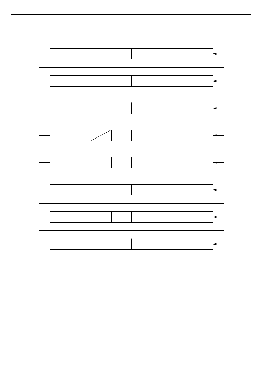
TIME CHIP REGISTER DEFINITION Figure 5
REGISTER
7654 3210
0
0.1 SEC
0.01 SEC
RANGE
(BCD)
00–99
DS1315
1
2
3
4
5
6
7
0
0
12/24 0
00 0
00
0 0 0 10 MONTH
10 SEC SECONDS
10 MIN MINUTES
10
OSC RST
10 YEAR YEAR
HR
A/P
10 DATE DATE
MONTH
HOUR
DAY
00–59
00–59
01–12
00–23
01–07
01–31
01–12
00–99
041697 7/22
Page 8

DS1315
ABSOLUTE MAXIMUM RATINGS*
Voltage on any Pin Relative to Ground –0.3V to +7.0V
Operating T emperature, commercial range 0°C to 70°C
Operating T emperature, industrial range –45°C to +85°C
Storage Temperature –55°C to +125°C
Soldering Temperature 260°C for 10 seconds
* This is a stress rating only and functional operation of the device at these or any other conditions above those
indicated in the operation sections of this specification is not implied. Exposure to absolute maximum rating
conditions for extended periods of time may affect reliability.
RECOMMENDED DC OPERATING CONDITIONS (0°C to 70°C)
PARAMETER SYMBOL MIN TYP MAX UNITS NOTES
Power Supply Voltage 5 Volt
Operation
Power Supply Voltage 3.3 Volt
Operation
Input Logic 1 V
Input Logic 0 V
Battery Voltage V
BAT1
or V
BAT2
V
V
V
CC
V
CC
IH
BAT1
BAT2
4.5 5.0 5.5 V 1
3.0 3.3 3.6 V 1
2.2 V
IL
–0.3 +0.6 V 1
,
2.5 3.7 V
+ 0.3 V 1
CC
DC OPERATING ELECTRICAL CHARACTERISTICS (0°C to 70°C; VCC = 5.0 ± 10%)
PARAMETER SYMBOL MIN TYP MAX UNITS NOTES
Average VCC Power Supply
Current
VCC Power Supply Current,
= V
(V
CCO
CCI
–0.3)
TTL Standby Current (CEI = VIH) I
CMOS Standby Current
= V
(CEI
CCI
–0.2)
Input Leakage Current (any input) I
Output Leakage Current (any
output)
Output Logic 1 Voltage
= –1.0 mA)
(I
OUT
Output Logic 0 Voltage
= 4.0 mA)
(I
OUT
Power–Fail Trip Point V
Battery Switch Voltage V
I
CC1
I
CC01
CC2
I
CC3
I
V
V
IL
OL
OH
OL
PF
SW
5 mA 6
150 mA 7
3 mA 6
1 mA 6
–1 +1 µA 10
–1 +1 µA
2.4 V 2
0.4 V 2
4.25 4.5 V
V
,
BAT1
V
BAT2
13
041697 8/22
Page 9

DS1315
DC POWER DOWN ELECTRICAL CHARACTERISTICS (0°C to 70°C; VCC < 4.5V)
PARAMETER SYMBOL MIN TYP MAX UNITS NOTES
CEO Output Voltage V
V
BAT1
or V
Battery Current I
BAT2
Battery Backup Current
= V
@ V
CCO
BAT
–0.2V
CEO
BAT
I
CCO2
V
or V
CCI
–0.2
–0.2
BAT1,2
V 8
0.5 µA 6
10 µA 9
AC ELECTRICAL OPERATING CHARACTERISTICS
ROM/RAM
PARAMETER SYMBOL MIN TYP MAX UNITS NOTES
Read Cycle Time t
CEI Access Time t
OE Access Time t
CEI to Output Low Z t
OE to Output Low Z t
CEI to Output High Z t
OE to Output High Z t
Read Recovery t
Write Cycle t
Write Pulse Width t
Write Recovery t
Data Setup t
Data Hold Time t
CEI Pulse Width t
OE Pulse Width t
RST Pulse Width t
CEI Propagation Delay t
CEI High to Power–Fail t
= GND (0°C to 70°C; VCC = 5.0 ± 10%)
RC
CO
OE
COE
OEE
OD
ODO
RR
WC
WP
WR
DS
DH
CW
OW
RST
PD
PF
65 ns
55 ns
55 ns
5 ns
5 ns
25 ns
25 ns
10 ns
65 ns
55 ns
10 ns 4
30 ns 5
0 ns 5
60 ns
55 ns
65 ns
5 ns 2, 3, 11
0 ns 11
041697 9/22
Page 10

DS1315
AC ELECTRICAL OPERATING CHARACTERISTICS
ROM/RAM
= V
CCO
PARAMETER SYMBOL MIN TYP MAX UNITS NOTES
Read Cycle Time t
CEI Access Time t
OE Access Time t
CEI to Output Low Z t
OE to Output Low Z t
CEI to Output High Z t
OE to Output High Z t
Address Setup Time t
Address Hold Time t
Read Recovery t
Write Cycle t
CEI Pulse Width t
OE Pulse Width t
Write Recovery t
Data Setup t
Data Hold Time t
RST Pulse Width t
CEI Propagation Delay t
CEI High to Power–Fail t
RC
CO
OE
COE
OEE
OD
ODO
AS
AH
RR
WC
CW
OW
WR
DS
DH
RST
PD
PF
65 ns
5 ns
5 ns
5 ns
5 ns
10 ns
65 ns
55 ns
55 ns
10 ns 4
30 ns 5
0 ns 5
65 ns
(0°C to 70°C; VCC = 5.0 ± 10%)
55 ns
55 ns
25 ns
25 ns
5 ns 2, 3, 11
0 ns 11
3.3 VOLT DEVICE OPERATING RANGE CHARACTERISTICS
DC OPERATING ELECTRICAL CHARACTERISTICS (0°C to 70°C; V
PARAMETER SYMBOL MIN TYP MAX UNITS NOTES
Average VCC Power Supply
Current
Average VCC Power Supply
= V
Current, (V
CCO
CCI
–0.3)
TTL Standby Current (CEI = VIH) I
CMOS Standby Current
= V
(CEI
CCI
–0.2)
Input Leakage Current (any input) I
Output Leakage Current (any
output)
041697 10/22
I
CC1
I
CC01
CC2
I
CC3
I
LO
3 mA 6
100 mA 7
2 mA 6
1 mA 6
IL
–1 +1 µA
–1 +1 µA
= 3.3 ± 10%)
CC
Page 11

DS1315
DC OPERATING ELECTRICAL CHARACTERISTICS (cont’d) (0°C to 70°C; VCC = 3.3 ±10%)
PARAMETER SYMBOL MIN TYP MAX UNITS NOTES
Output Logic 1 Voltage
= 0.4 mA)
(I
OUT
Output Logic 0 Voltage
= 1.6 mA)
(I
OUT
Power–Fail Trip Point V
Battery Switch Voltage V
V
OH
V
OL
PF
SW
2.4 V 2
0.4 V 2
2.8 3.0 V
V
,
BAT1
V
BAT2
13
DC POWER DOWN ELECTRICAL CHARACTERISTICS (0°C to 70°C; VCC < 2.7V)
PARAMETER SYMBOL MIN TYP MAX UNITS NOTES
V
or
CCI
CEO Output Voltage V
V
BAT1
or V
Battery Current I
BAT2
Battery Backup Current
V
@ V
CCO =
BAT
–0.2
CEO
BAT
I
CCO2
V
BAT1,2
–0.2
V 8
0.3 µA 6
10 µA 9
041697 11/22
Page 12

DS1315
AC ELECTRICAL OPERATING CHARACTERISTICS
ROM/RAM
PARAMETER SYMBOL MIN TYP MAX UNITS NOTES
Read Cycle Time t
CEI Access Time t
OE Access Time t
CEI to Output Low Z t
OE to Output Low Z t
CEI to Output High Z t
OE to Output High Z t
Read Recovery t
Write Cycle t
Write Pulse Width t
Write Recovery t
Data Setup t
Data Hold Time t
CEI Pulse Width t
OE Pulse Width t
RST Pulse Width t
CEI Propagation Delay t
CEI High to Power–Fail t
= GND (0°C to 70°C; VCC = 3.3 ± 10%)
RC
CO
OE
COE
OEE
OD
ODO
RR
WC
WP
WR
DS
DH
CW
OW
RST
PD
PF
120 ns
100 ns
100 ns
5 ns
5 ns
40 ns
40 ns
20 ns
120 ns
100 ns
20 ns 4
45 ns 5
0 ns 5
105 ns
100 ns
120 ns
10 ns 2, 3, 12
0 ns 12
041697 12/22
Page 13

DS1315
AC ELECTRICAL OPERATING CHARACTERISTICS
ROM/RAM
= V
CCO
PARAMETER SYMBOL MIN TYP MAX UNITS NOTES
Read Cycle Time t
CEI Access Time t
OE Access Time t
CEI to Output Low Z t
OE to Output Low Z t
CEI to Output High Z t
OE to Output High Z t
Address Setup Time t
Address Hold Time t
Read Recovery t
Write Cycle t
CEI Pulse Width t
OE Pulse Width t
Write Recovery t
Data Setup t
Data Hold Time t
RST Pulse Width t
CEI Propagation Delay t
RC
CO
OE
COE
OEE
OD
ODO
AS
AH
RR
WC
CW
OW
WR
DS
DH
RST
PD
120 ns
5 ns
5 ns
10 ns
10 ns
20 ns
120 ns
100 ns
100 ns
20 ns 4
45 ns 5
0 ns 5
120 ns
(0°C to 70°C; VCC = 3.3 ± 10%)
100 ns
100 ns
40 ns
40 ns
5 ns 2, 3, 12
CAPACITANCE (tA = 25°C)
PARAMETER SYMBOL MIN TYP MAX UNITS NOTES
Input Capacitance C
Output Capacitance C
IN
OUT
10 pF
10 pF
041697 13/22
Page 14

DS1315
TIMING DIAGRAM: READ CYCLE TO TIME CHIP ROM/RAM = GND Figure 6
WE
= V
IH
t
CEI
OE
RC
t
CO
t
CW
t
OE
t
OW
t
OEE
t
COE
t
t
ODO
RR
t
OD
Q
OUTPUT DATA VALID
TIMING DIAGRAM: WRITE CYCLE TO TIME CHIP ROM/RAM = GND Figure 7
OE
= V
IH
t
WE
t
WP
WC
t
WR
041697 14/22
CEI
D
t
CW
t
DS
DATA IN STABLE
t
WR
t
DH
t
DH
Page 15

DS1315
TIMING DIAGRAM: READ CYCLE TO TIME CHIP ROM/RAM = V
t
RC
t
CO
CEI
OE
WE
t
t
AS
AS
t
OEE
t
COE
Q
t
CW
t
t
OE
t
OW
RC
t
AH
OUTPUT DATA VALID
TIMING DIAGRAM: WRITE CYCLE TO TIME CHIP ROM/RAM = V
t
WC
t
CW
CEI
CCO
CCO
Figure 8
t
RR
t
OD
t
RR
t
ODO
t
AH
Figure 9
t
WR
OE
WE
t
t
WC
t
OW
t
AS
t
AS
t
DS
t
DS
D
DATA IN STABLE
t
t
WR
t
AH
AH
t
DH
DH
041697 15/22
Page 16

DS1315
TIMING DIAGRAM: RESET PULSE Figure 10
t
RST
RST
5V DEVICE POWER–UP POWER–DOWN CHARACTERISTICS,
ROM/RAM
= V
PARAMETER SYMBOL MIN TYP MAX UNITS NOTES
Recovery Time at
Power–Up
VCC Slew Rate Power–
Down
VCC Slew Rate Power–
Down
VCC Slew Rate Power–
UP
CEI High to Power–Fail t
OR GND (0°C to 70°C)
CCO
t
REC
VCC>4.5
4.0 ≤ V
4.5
t
3.0 ≤ V
4.0
4.5 ≤ V
4.0
t
FB
t
PF
F
≤
CC
300 mS 11
10 mS 11
≤
CC
R
≤
CC
0 mS 11
2 mS 11
0 mS 11
5V DEVICE POWER–UP CONDITION Figure 1 1
CEI
t
REC
4.5V
4.25V
041697 16/22
ROM/RAM = GND
= V
ROM/RAM
CCO
4.0V
V
CCI
BAT - 0.2V
CEO
CEO
t
R
t
CE
V
IL
t
PD
t
CE
Page 17

5V DEVICE POWER–DOWN CONDITION Figure 12
t
CEI
CE
DS1315
t
PF
V
- 0.2V
BAT
4.25V
t
F
4.0V
V
BAT1,2
t
FB
ROM/RAM = GND
= V
ROM/RAM
CCO
CEO
CEO
V
CCI
t
PD
t
CE
4.5V
3.3V DEVICE POWER–UP POWER–DOWN CHARACTERISTICS,
ROM/RAM
= V
PARAMETER SYMBOL MIN TYP MAX UNITS NOTES
Recovery Time at
Power–Up
VCC Slew Rate Power–
Down
VCC Slew Rate Power–
UP
CEI High to Power–Fail t
OR GND (0°C to 70°C)
CCO
t
VCC>3
2.9 ≤ V
3 ≤ V
REC
t
F
t
R
CC
PF
CC
≤ 2.9
≤ 3
300 ms 12
0 ms 12
0 ms 12
2 ms 12
041697 17/22
Page 18

DS1315
3.3V DEVICE POWER–UP CONDITION Figure 13
CEI
t
REC
t
CE
V
IL
2.7V
2.6V
2.5V
V
CCI
t
R
BAT - 0.2V
CCO
CEO
CEO
ROM/RAM = GND
= V
ROM/RAM
3.3V DEVICE POWER–DOWN CONDITION Figure 14
t
CE
t
PD
t
CE
ROM/RAM = GND
CEI
CEO
t
PD
t
CE
t
PF
V
- 0.2V
BAT
ROM/RAM
041697 18/22
= V
CCO
CEO
V
CCI
2.7V
2.6V
2.5V
t
F
Page 19

NOTES:
1. All voltages are referenced to ground.
2. Measured with load shown in Figure 15.
3. Input pulse rise and fall times equal 10 ns.
is a function of the latter occurring edge of WE or CE in RAM mode, or OE or CE in ROM mode.
4. t
WR
5. t
DH
and t
are functions of the first occurring edge of WE or CE in RAM mode, or OE or CE in ROM mode.
DS
6. Measured without RAM connected.
7. I
8. Applies to CEO
9. I
10.Applies to all input pins except RST
is the maximum average load current the DS1315 can supply to external memory.
CC01
with the ROM/RAM pin grounded. When the ROM/RAM pin is connected to V
to a low level as V
is the maximum average load current that the DS1315 can supply to memory in the battery backup mode.
CC02
falls below V
CCI
.
BAT
. RST is pulled internally to V
CCI
.
11.See Figures 11 and 12.
12.See Figures 13 and 14.
is determined by the larger of V
13.V
SW
BAT1
and V
BAT2
.
OUTPUT LOAD Figure 15
, CEO will go
CCO
DS1315
680
V
CCI
1.1K
50 pF
041697 19/22
Page 20

DS1315
DS1315 TIME CHIP 16–PIN DIP
B D
1
A
C
F
K
E
G
J
H
16–PINPKG
DIM MIN MAX
A IN. 0.740 0.780
MM
B IN. 0.240 0.260
MM
C IN. 0.120 0.140
MM
D IN. 0.300 0.325
MM
E IN. 0.015 0.040
MM
F IN. 0.110 0.140
MM
G IN. 0.090 0.110
MM
H IN. 0.300 0.370
MM
J IN. 0.008 0.012
MM
K IN. 0.015 0.021
MM
041697 20/22
Page 21

DS1315 TIME CHIP 16–PIN SOIC
GK
B
1
A
C
DS1315
H
F
E
PKG 16–PIN
DIM MIN MAX
A IN.MM0.402
B IN.MM0.290
C IN.MM0.089
E IN.MM0.004
F IN.MM0.094
G IN.
MM
H INMM0.398
J INMM0.009
K IN.MM0.013
L INMM0.016
PHI 0° 8°
10.21
7.37
2.26
0.102
2.38
0.050 BSC
1.27 BSC
10.11
0.229
0.33
0.40
0.412
10.46
0.300
7.65
0.095
2.41
0.012
0.30
0.105
2.68
0.416
10.57
0.013
0.33
0.019
0.48
0.040
1.02
phi
J
L
041697 21/22
Page 22

DS1315
DS1315 TIME CHIP 20–PIN TSSOP
D
n
B
e1
DIM MIN MAX
A MM – 1.10
A1 MM 0.05 –
A2 MM 0.75 1.05
C MM 0.09 0.18
L MM 0.50 0.70
e1 MM 0.65 BSC
B MM 0.18 0.30
D MM 6.40 6.90
E MM 4.40 NOM
G MM 0.25 REF
H MM 6.25 6.55
phi 0° 8°
56–G2010–000
E
H
SEE DETAIL A
c
A2
A1
L
DETAIL A
phi
G
A
041697 22/22
 Loading...