

Page 1
www.maxim-ic.com
DS1305
Serial Alarm Real-Time Clock
FEATURES
§ Real-time clock (RTC) counts seconds,
minutes, hours, date of the month, month,
day of the week, and year with leap-year
compensation valid up to 2100
§ 96-byte, battery-backed NV RAM for data
storage
§ Two time-of-day alarms, programmable on
combination of seconds, minutes, hours, and
day of the week
§ Serial interface supports Motorola SPI
(serial peripheral interface) serial data ports
or standard 3-wire interface
§ Burst mode for reading/writing successive
addresses in clock/RAM
§ Dual-power supply pins for primary and
backup power supplies
§ Optional trickle charge output to backup
supply
§ 2.0V to 5.5V operation
§ Optional industrial temperature range:
-40°C to +85°C
§ Available in space-efficient, 20-pin TSSOP
package
§ Underwriters Laboratory (UL) recognized
™
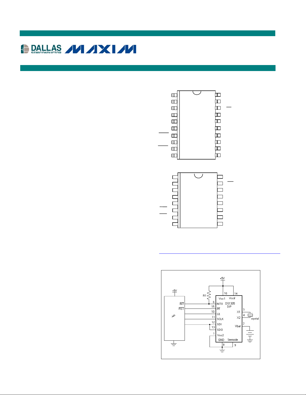
PIN ASSIGNMENT
V
CC2
V
BAT
X1 3 18 PF
NC 4 17 V
X2 5 16 SD0
NC 6 15 SDI
INT0 7 14 SCLK
NC 8 13 NC
INT1 9 12 CE
GND 10 11 SERMODE
DS1305 20-Pin TSSOP (4.4mm)
V
CC2
V
BAT
X1 3 14 V
X2 4 13 SDO
NC 5 12 SDI
INT0 6 11 SCLK
INT1 7 10 CE
GND 8 9 SERMODE
DS1305 16-Pin DIP (300mil)
Package dimension information can be found at:
http://www.maxim-ic.com/TechSupport/DallasPackInfo.htm
120V
219NC
1 16 V
215PF
CC1
CCIF
CC1
CCIF
ORDERING INFORMATION
DS1305 16-Pin DIP (300mil)
DS1305N 16-Pin DIP (Industrial)
DS1305E 20-Pin TSSOP (173mil)
DS1305EN 20-Pin TSSOP (Industrial)
SPI is a trademark of Motorola, Inc.
TYPICAL OPERATING CIRCUIT
1 of 20 061202
Page 2

DS1305
PIN DESCRIPTION
V
CC1
V
- Backup Power Supply
CC2
V
- +3V Battery Input
BAT
V
- Interface Logic Power-Supply Input
CCIF
GND - Ground
X1, X2 - 32,768kHz Crystal Connection
INT0 - Interrupt 0 Output
INT1 - Interrupt 1 Output
SDI - Serial Data In
SDO - Serial Data Out
CE - Chip Enable
SCLK - Serial Clock
SERMODE - Serial Interface Mode
PF - Power-Fail Output
- Primary Power Supply
DESCRIPTION
The DS1305 serial alarm real-time clock provides a full binary coded decimal (BCD) clock calendar that
is accessed by a simple serial interface. The clock/calendar provides seconds, minutes, hours, day, date,
month, and year information. The end of the month date is automatically adjusted for months with fewer
than 31 days, including corrections for leap year. The clock operates in either the 24-hour or 12-hour
format with AM/PM indicator. In addition, 96 bytes of NV RAM are provided for data storage.
An interface logic power-supply input pin (V
) allows the DS1305 to drive SDO and PF pins to a level
CCIF
that is compatible with the interface logic. This allows an easy interface to 3V logic in mixed supply
systems.
The DS1305 offers dual-power supplies as well as a battery input pin. The dual power supplies support a
programmable trickle charge circuit that allows a rechargeable energy source (such as a super cap or
rechargeable battery) to be used for a backup supply. The V
pin allows the device to be backed up by
BAT
a non-rechargeable battery. The DS1305 is fully operational from 2.0V to 5.5V.
Two programmable time-of-day alarms are provided by the DS1305. Each alarm can generate an
interrupt on a programmable combination of seconds, minutes, hours, and day. “Don’t care” states can be
inserted into one or more fields if it is desired for them to be ignored for the alarm condition. The time-ofday alarms can be programmed to assert two different interrupt outputs or to assert one common interrupt
output. Both interrupt outputs operate when the device is powered by V
CC1
CC2
, or V
BAT
.
, V
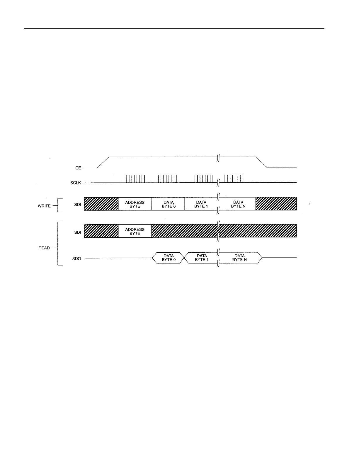
The DS1305 supports a direct interface to SPI serial data ports or standard 3-wire interface. A
straightforward address and data format is implemented in which data transfers can occur 1 byte at a time
or in multiple-byte-burst mode.
2 of 20
Page 3
DS1305
OPERATION
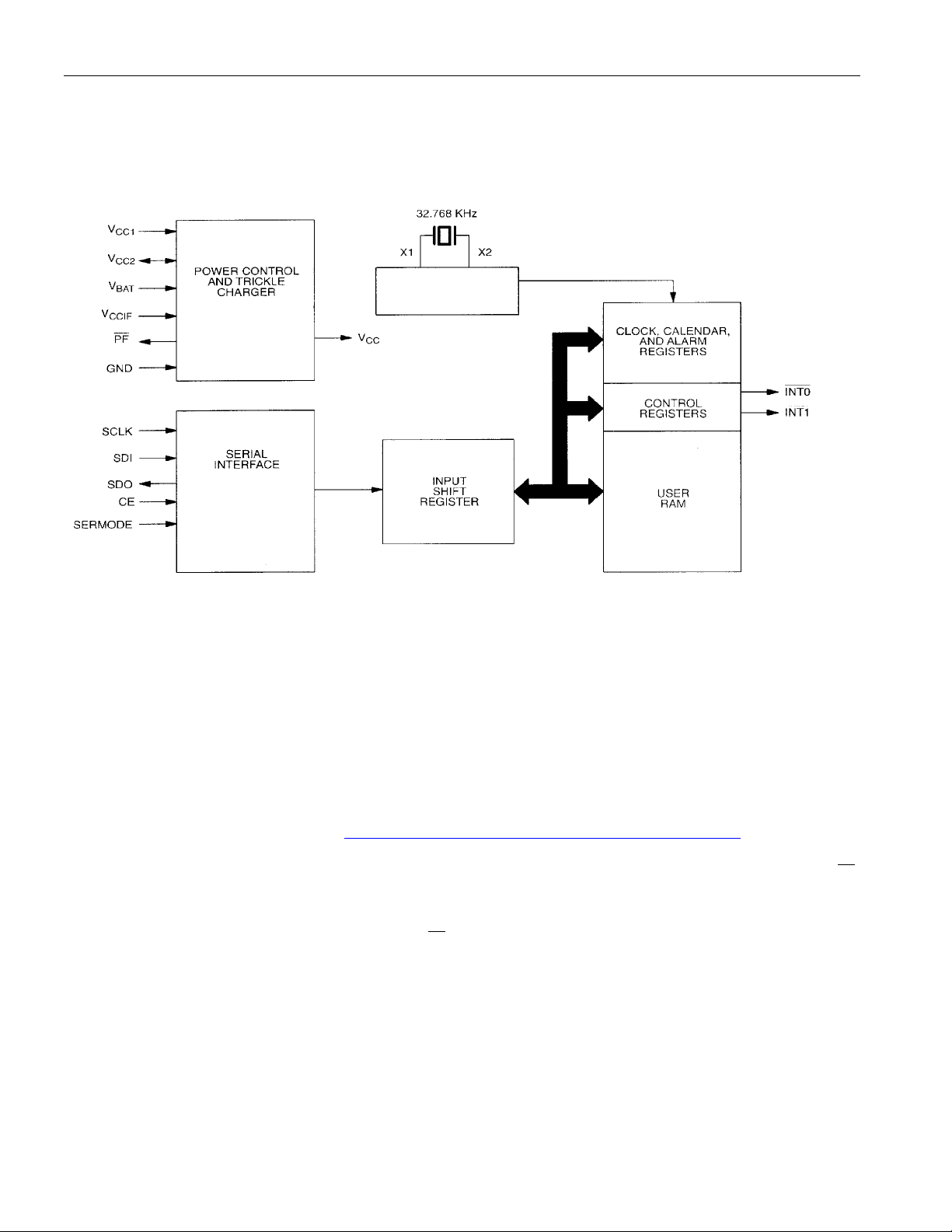
The block diagram in Figure 1 shows the main elements of the serial alarm RTC. The following
paragraphs describe the function of each pin.
Figure 1. BLOCK DIAGRAM
OSCILLATOR AND
COUNTDOWN CHAIN
1Hz
SIGNAL DESCRIPTIONS
V
– DC power is provided to the device on this pin. V
CC1
V
– This is the secondary power supply pin. In systems using the trickle charger, the rechargeable
CC2
energy source is connected to this pin.
is the primary power supply.
CC1
V
– Battery input for any standard 3V lithium cell or other energy source. UL recognized to ensure
BAT
against reverse charging current when used in conjunction with a lithium battery.
See “Conditions of Acceptability” at http://www.maxim-ic.com/TechSupport/QA/ntrl.htm.
V
(Interface Logic Power-Supply Input) – The V
CCIF
pin allows the DS1305 to drive SDO and PF
CCIF
output pins to a level that is compatible with the interface logic, thus allowing an easy interface to 3V
logic in mixed supply systems. This pin is physically connected to the source connection of the p-channel
transistors in the output buffers of the SDO and
PF pins.
SERMODE (Serial Interface Mode Input) – The SERMODE pin offers the flexibility to choose
between two serial interface modes. When connected to GND, standard 3-wire communication is
selected. When connected to VCC, SPI communication is selected.
SCLK (Serial Clock Input) – SCLK is used to synchronize data movement on the serial interface for
either the SPI or 3-wire interface.
3 of 20
Page 4

DS1305
SDI (Serial Data Input) – When SPI communication is selected, the SDI pin is the serial data input for
the SPI bus. When 3-wire communication is selected, this pin must be tied to the SDO pin (the SDI and
SDO pins function as a single I/O pin when tied together).
SDO (Serial Data Output) – When SPI communication is selected, the SDO pin is the serial data output
for the SPI bus. When 3-wire communication is selected, this pin must be tied to the SDI pin (the SDI and
SDO pins function as a single I/O pin when tied together).
CE (Chip Enable) – The chip enable signal must be asserted high during a read or a write for both 3wire and SPI communication. This pin has an internal 55k pulldown resistor (typical).
INT0 (Interrupt 0 Output) – The INT0 pin is an active low output of the DS1305 that can be used as an
interrupt input to a processor. The INT0 pin can be programmed to be asserted by only Alarm 0 or can be
programmed to be asserted by either Alarm 0 or Alarm 1. The
INT0 pin remains low as long as the status
bit causing the interrupt is present and the corresponding interrupt enable bit is set. The
when the DS1305 is powered by V
CC1
, V
CC2
, or V
. The INT0 pin is an open drain output and requires
BAT
INT0 pin operates
an external pullup resistor.
INT1 (Interrupt 1 Output) – The INT1 pin is an active-low output of the DS1305 that can be used as an
interrupt input to a processor. The INT1 pin can be programmed to be asserted by Alarm 1 only. The
INT1 pin remains low as long as the status bit causing the interrupt is present and the corresponding
interrupt enable bit is set. The INT1 pin operates when the DS1305 is powered by V
CC1
, V
CC2
, or V
BAT
The INT1 pin is an open-drain output and requires an external pullup resistor.
Both INT0 and INT1are open-drain outputs. The two interrupts and the internal clock continue to run
regardless of the level of VCC (as long as a power source is present).
PF (Power-Fail Output) – The PF pin is used to indicate loss of the primary power supply (V
When V
is less than V
CC1
or is less than V
CC2
, the PF pin is driven low.
BAT
CC1
X1, X2 – Connections for a standard 32.768kHz quartz crystal. The internal oscillator is designed for
operation with a crystal having a specified load capacitance of 6pF. For more information on crystal
selection and crystal layout considerations, refer to Application Note 58, “Crystal Considerations with
Dallas Real-Time Clocks.” The DS1305 can also be driven by an external 32.768kHz oscillator. In this
configuration, the X1 pin is connected to the external oscillator signal and the X2 pin is floated.
.
).
4 of 20
Page 5

DS1305
RECOMMENDED LAYOUT FOR CRYSTAL
CLOCK ACCURACY
The accuracy of the clock is dependent upon the accuracy of the crystal and the accuracy of the match
between the capacitive load of the oscillator circuit and the capacitive load for which the crystal was
trimmed. Additional error is added by crystal frequency drift caused by temperature shifts. External
circuit noise coupled into the oscillator circuit can result in the clock running fast. Refer to Application
Note 58, “Crystal Considerations with Dallas Real-Time Clocks” for detailed information.
CLOCK, CALENDAR, AND ALARM
The time and calendar information is obtained by reading the appropriate register bytes. The RTC
registers and user RAM are illustrated in Figure 2. The time, calendar, and alarm are set or initialized by
writing the appropriate register bytes. Note that some bits are set to 0. These bits always read 0 regardless
of how they are written. Also note that registers 12h to 1Fh (read) and registers 92h to 9Fh are reserved.
These registers always read 0 regardless of how they are written. The contents of the time, calendar, and
alarm registers are in the BCD format.
Except where otherwise noted, the initial power on state of all registers is not defined. Therefore, it is
important to enable the oscillator (EOSC = 0) and disable write protect (WP = 0) during initial
configuration.
WRITING TO THE CLOCK REGISTERS
The internal time and date registers continue to increment during write operations. However, the
countdown chain is reset when the seconds register is written. Writing the time and date registers within
one second after writing the seconds register ensures consistent data.
Terminating a write before the last bit is sent aborts the write for that byte.
READING FROM THE CLOCK REGISTERS
Buffers are used to copy the time and date register at the beginning of a read. When reading in burst
mode, the user copy is static while the internal registers continue to increment.
5 of 20
Page 6

Figure 2. RTC REGISTERS AND ADDRESS MAP
DS1305
HEX ADDRESS
READ WRITE
00H 80H 0 10-SEC SEC 00–59
01H 81H 0 10-MIN MIN 00–59
02H 82H 0
03H 83H 0 0 0 0 DAY 1–7
04H 84H 0 0 10-DATE DATE 1–31
05H 85H 0 0 10-MONTH MONTH 01–12
06H 86H 10 YEAR YEAR 00–99
——
07H 87H M 10-SEC ALARM SEC ALARM 00–59
08H 88H M 10-MIN ALARM MIN ALARM 00–59
09H 89H M
0AH 8AH M 0 0 0 DAY ALARM 01–07
——
0BH 8BH M 10-SEC ALARM SEC ALARM 00–59
0CH 8CH M 10-MIN ALARM MIN ALARM 00–59
0DH 8DH M
0EH 8EH M 0 0 0 DAY ALARM 01–07
0FH 8FH CONTROL REGISTER —
10H 90H STATUS REGISTER —
11H 91H TRICKLE CHARGER REGISTER —
12–1FH 92–9FH RESERVED —
20–7FH A0–FFH 96 BYTES USER RAM 00–FF
Bit7 Bit6 Bit5 Bit4 Bit3 Bit2 Bit1 Bit0 RANGE
12
24 10
12
24 10
12
24 10
P 01–12 + P/A
A
P
A
P
A
10-HR HOURS
ALARM 0
10 HR HOUR ALARM
ALARM 1
10 HR HOUR ALARM
00–23
—
01–12 + P/A
00–23
—
01–12 + P/A
00–23
Note: Range for alarm registers does not include mask’m’ bits.
The DS1305 can be run in either 12-hour or 24-hour mode. Bit 6 of the hours register is defined as the
12- or 24-hour mode select bit. When high, the 12-hour mode is selected. In the 12-hour mode, bit 5 is the
AM/PM bit with logic high being PM. In the 24-hour mode, bit 5 is the second 10-hour bit (20 to 23
hours).
The DS1305 contains two time-of-day alarms. Time-of-day Alarm 0 can be set by writing to registers 87h
to 8Ah. Time-of-day Alarm 1 can be set by writing to registers 8Bh to 8Eh. The alarms can be
programmed (by the INTCN bit of the control register) to operate in two different modes; each alarm can
drive its own separate interrupt output or both alarms can drive a common interrupt output. Bit 7 of each
of the time-of-day alarm registers are mask bits (Table 1). When all of the mask bits are logic 0, a timeof-day alarm only occurs once per week when the values stored in timekeeping registers 00h to 03h
match the values stored in the time-of-day alarm registers. An alarm is generated every day when bit 7 of
the day alarm register is set to a logic 1. An alarm is generated every hour when bit 7 of the day and hour
alarm registers is set to a logic 1. Similarly, an alarm is generated every minute when bit 7 of the day,
hour, and minute alarm registers is set to a logic 1. When bit 7 of the day, hour, minute, and seconds
alarm registers is set to a logic 1, alarm occurs every second.
6 of 20
Page 7

DS1305
During each clock update, the RTC compares the Alarm 0 and Alarm 1 registers with the corresponding
clock registers. When a match occurs, the corresponding alarm flag bit in the status register is set to a 1. If
the corresponding alarm interrupt enable bit is enabled, an interrupt output is activated.
Table 1. TIME-OF-DAY ALARM MASK BITS
ALARM REGISTER MASK BITS (BIT 7)
SECONDS MINUTES HOURS DAYS
1 1 1 1 Alarm once per second
0 1 1 1 Alarm when seconds match
0 0 1 1 Alarm when minutes and seconds match
0 0 0 1 Alarm hours, minutes, and seconds match
0 0 0 0 Alarm day, hours, minutes and seconds match
FUNCTION
SPECIAL PURPOSE REGISTERS
The DS1305 has three additional registers (control register, status register, and trickle charger register)
that control the RTC, interrupts, and trickle charger.
CONTROL REGISTER (READ 0FH, WRITE 8FH)
BIT7 BIT6 BIT5 BIT4 BIT3 BIT2 BIT1 BIT0
EOSC
EOSC (Enable Oscillator) – This bit when set to logic 0 startS the oscillator. When this bit is set to a
logic 1, the oscillator is stopped and the DS1305 is placed into a low-power standby mode with a current
drain of less than 100nA when power is supplied by V
defined.
WP 0 0 0 INTCN AIE1 AIEO
BAT
or V
. The initial power-on state is not
CC2
WP (Write Protect) – Before any write operation to the clock or RAM, this bit must be logic 0. When
high, the write protect bit prevents a write operation to any register, including bits 0, 1, 2, and 7 of the
control register. Upon initial power-up, the state of the WP bit is undefined. Therefore, the WP bit should
be cleared before attempting to write to the device.
INTCN (Interrupt Control) – This bit controls the relationship between the two time-of-day alarms and
the interrupt output pins. When the INTCN bit is set to a logic 1, a match between the timekeeping
registers and the Alarm 0 registers activates the INT0 pin (provided that the alarm is enabled) and a
match between the timekeeping registers and the Alarm 1 registers activate the INT1 pin (provided that
the alarm is enabled). When the INTCN bit is set to a logic 0, a match between the timekeeping registers
and either Alarm 0 or Alarm 1 activate the
INT0 pin (provided that the alarms are enabled). INT1 has no
function when INTCN is set to a logic 0.
AIE0 (Alarm Interrupt Enable 0) – When set to a logic 1, this bit permits the interrupt 0 request flag
(IRQF0) bit in the status register to assert
not initiate the
INT0 signal.
INT0 . When the AIE0 bit is set to logic 0, the IRQF0 bit does
AIE1 (Alarm Interrupt Enable 1) – When set to a logic 1, this bit permits the interrupt 1 request flag
(IRQF1) bit in the status register to assert
INT1 (when INTCN = 1) or to assert INT0 (when INTCN = 0).
When the AIE1 bit is set to logic 0, the IRQF1 bit does not initiate an interrupt signal.
7 of 20
Page 8
DS1305
STATUS REGISTER (READ 10H)
BIT7 BIT6 BIT5 BIT4 BIT3 BIT2 BIT1 BIT0
000000IRQF1IRQF0
IRQF0 (Interrupt 0 Request Flag) – A logic 1 in the interrupt request flag bit indicates that the current
time has matched the Alarm 0 registers. If the AIE0 bit is also a logic 1, the INT0 pin goes low. IRQF0 is
cleared when the address pointer goes to any of the Alarm 0 registers during a read or write.
IRQF1 (Interrupt 1 Request Flag) – A logic 1 in the interrupt request flag bit indicates that the current
time has matched the Alarm 1 registers. This flag can be used to generate an interrupt on either
INT1 depending on the status of the INTCN bit in the control register. If the INTCN bit is set to a logic 1
INT0 or
and IRQF1 is at a logic 1 (and AIE1 bit is also a logic 1), the INT1 pin goes low. If the INTCN bit is set
to a logic 0 and IRQF1 is at a logic 1 (and AIE1 bit is also a logic 1), the
INT0 pin goes low. IRQF1 is
cleared when the address pointer goes to any of the Alarm 1 registers during a read or write.
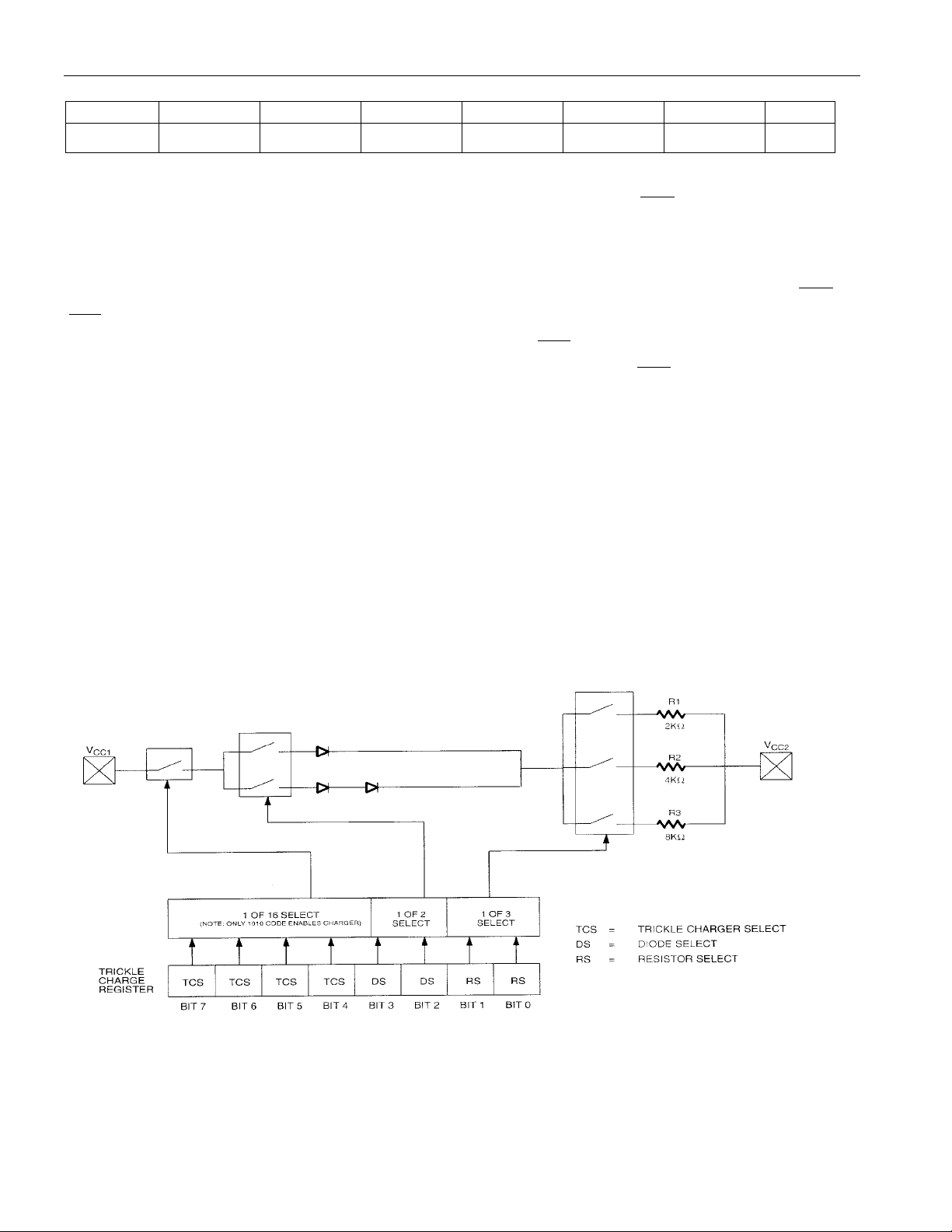
TRICKLE CHARGE REGISTER (READ 11H, WRITE 91H)
This register controls the trickle charge characteristics of the DS1305. The simplified schematic of Figure
3 shows the basic components of the trickle charger. The trickle-charge select (TCS) bits (bits 4–7)
control the selection of the trickle charger. To prevent accidental enabling, only a pattern of 1010 enables
the trickle charger. All other patterns disable the trickle charger. On the initial application of power, the
DS1305 powers up with the trickle charger disabled. The diode select (DS) bits (bits 2–3) select whether
one diode or two diodes are connected between V
resistor that is connected between V
CC1
and V
CC2
CC1
and V
. The resistor select (RS) bits select the
CC2
. The resistor and diodes are selected by the RS and DS
bits, as shown in Table 2.
Figure 3. PROGRAMMABLE TRICKLE CHARGER
8 of 20
Page 9

Table 2. TRICKLE CHARGER RESISTOR AND DIODE SELECT
DS1305
TCS
Bit 7
X X XXXX0 0 Disabled
X X XX0 0 XX Disabled
X X XX1 1 XX Disabled
1 0 100101 1 Diode, 2kΩ
1 0 100110 1 Diode, 4kΩ
1 0 100111 1 Diode, 8kΩ
1 0 101001 2 Diodes, 2kΩ
1 0 101010 2 Diodes, 4kΩ
1 0 101011 2 Diodes, 8kΩ
TCS
Bit 6
TCS
Bit 5
TCS
Bit 4DSBit 3DSBit 2RSBit 1RSBit 0
FUNCTION
The user determines diode and resistor selection according to the maximum current desired for battery or
super cap charging. The maximum charging current can be calculated as illustrated in the following
example. Assume that a system power supply of 5V is applied to V
V
. Also assume that the trickle charger has been enabled with 1 diode and resister R1 between V
CC2
and V
. The maximum current I
CC2
would, therefore, be calculated as follows:
MAX
and a super cap is connected to
CC1
CC1
I
= (5.0V - diode drop) / R1 » (5.0V - 0.7V) / 2kW » 2.2mA
MAX
As the super cap charges, the voltage drop between V
CC1
and V
decreases and, therefore, the charge
CC2
current decreases.
POWER CONTROL
Power is provided through the V
are illustrated in Figure 4. Configuration 1 shows the DS1305 being backed up by a nonrechargeable
energy source such as a lithium battery. In this configuration, the system power supply is connected to
and V
V
CC1
accessible when V
is grounded. The DS1305 is write-protected if V
CC2
is greater than V
CC1
Configuration 2 illustrates the DS1305 being backed up by a rechargeable energy source. In this case, the
pin is grounded, V
V
BAT
is connected to the primary power supply, and V
CC1
secondary supply (the rechargeable energy source). The DS1305 operates from the larger of V
V
V
CC2
CC2
. When V
, V
powers the DS1305. The DS1305 does not write-protect itself in this configuration.
CC2
is greater than V
CC1
Configuration 3 shows the DS1305 in battery operate mode where the device is powered only by a single
battery. In this case, the V
CC1
and V
CC1
CC2
, V
BAT
, and V
CC2
+ 0.2V.
BAT
+ 0.2V (typical), V
pins. Three different power-supply configurations
BAT
is less than V
CC1
powers the DS1305. When V
CC1
BAT
CC2
pins are grounded and the battery is connected to the V
. The DS1305 is fully
is connected to the
or
CC1
is less than
CC1
pin.
CC2
Only these three configurations are allowed. Unused supply pins must be grounded.
9 of 20
Page 10
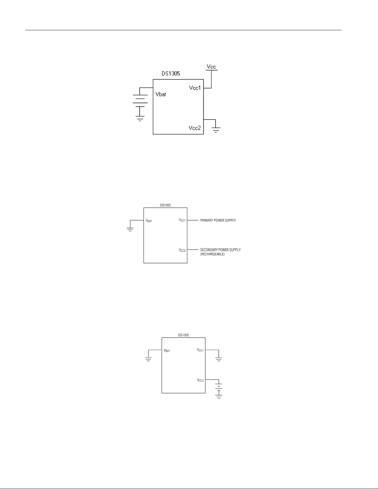
Figure 4. POWER SUPPLY CONFIGURATIONS
Configuration 1: Backup Supply is a Nonrechargeable Lithium Battery
V
CCTP
Note: Device is write-protected if VCC < V
Configuration 2: Backup Supply is a Rechargeable Battery or Super Capacitor
CCTP
.
DS1305
Note: Device does not provide automatic write protection.
Configuration 3: Battery Operate Mode
10 of 20
Page 11

DS1305
SERIAL INTERFACE
The DS1305 offers the flexibility to choose between two serial interface modes. The DS1305 can
communicate with the SPI interface or with a standard 3-wire interface. The interface method used is
determined by the SERMODE pin. When this pin is connected to VCC, SPI communication is selected.
When this pin is connected to ground, standard 3-wire communication is selected.
SERIAL PERIPHERAL INTERFACE (SPI)
The serial peripheral interface (SPI) is a synchronous bus for address and data transfer, and is used when
interfacing with the SPI bus on specific Motorola microcontrollers such as the 68HC05C4 and the
68HC11A8. The SPI mode of serial communication is selected by tying the SERMODE pin to VCC. Four
pins are used for the SPI. The four pins are the SDO (serial data out), SDI (serial data in), CE (chip
enable), and SCLK (serial clock). The DS1305 is the slave device in an SPI application, with the
microcontroller being the master.
The SDI and SDO pins are the serial data input and output pins for the DS1305, respectively. The CE
input is used to initiate and terminate a data transfer. The SCLK pin is used to synchronize data
movement between the master (microcontroller) and the slave (DS1305) devices.
The shift clock (SCLK), which is generated by the microcontroller, is active only during address and data
transfer to any device on the SPI bus. The inactive clock polarity is programmable in some
microcontrollers. The DS1305 determines the clock polarity by sampling SCLK when CE becomes
active. Therefore, either SCLK polarity can be accommodated. Input data (SDI) is latched on the internal
strobe edge and output data (SDO) is shifted out on the shift edge (Figure 5). There is one clock for each
bit transferred. Address and data bits are transferred in groups of eight.
11 of 20
Page 12

DS1305
Figure 5. SERIAL CLOCK AS A FUNCTION OF MICROCONTROLLER CLOCK
POLARITY (CPOL)
CE
CPOL = 1
SCLK
SHIFT DATA OUT (READ)
CPOL = 0
SCLK
SHIFT DATA OUT (READ)
DATA LATCH (WRITE)
DATA LATCH (WRITE)
1) CPHA bit polarity (if applicable) may need to be set accordingly.
2) CPOL is a bit that is set in the microcontroller’s control register.
3) SDO remains at high-Z until 8 bits of data are ready to be shifted out during a read.
ADDRESS AND DATA BYTES
Address and data bytes are shifted MSB first into the serial data input (SDI) and out of the serial data
output (SDO). Any transfer requires the address of the byte to specify a write or read to either a RTC or
RAM location, followed by one or more bytes of data. Data is transferred out of the SDO for a read
operation and into the SDI for a write operation (Figures 6 and 7).
Figure 6. SPI SINGLE-BYTE WRITE
Figure 7. SPI SINGLE-BYTE READ
*SCLK can be either polarity.
12 of 20
Page 13
DS1305
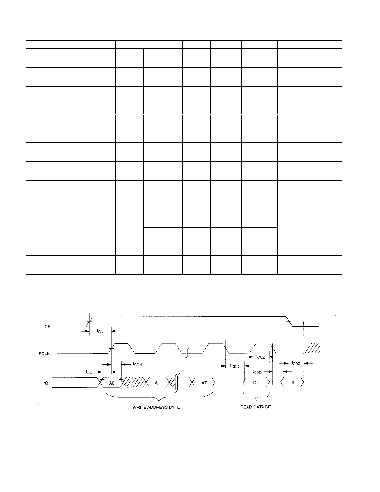
The address byte is always the first byte entered after CE is driven high. The most significant bit (A7) of
this byte determines if a read or write takes place. If A7 is 0, one or more read cycles occur. If A7 is 1,
one or more write cycles occur.
Data transfers can occur one byte at a time or in multiple-byte burst mode. After CE is driven high an
address is written to the DS1305. After the address, one or more data bytes can be written or read. For a
single-byte transfer, one byte is read or written and then CE is driven low. For a multiple-byte transfer,
however, multiple bytes can be read or written to the DS1305 after the address has been written. Each
read or write cycle causes the RTC register or RAM address to automatically increment. Incrementing
continues until the device is disabled. When the RTC is selected, the address wraps to 00h after
incrementing to 1Fh (during a read) and wraps to 80h after incrementing to 9Fh (during a write). When
the RAM is selected, the address wraps to 20h after incrementing to 7Fh (during a read) and wraps to
A0h after incrementing to FFh (during a write).
Figure 8. SPI MULTIPLE-BYTE BURST TRANSFER
READING AND WRITING IN BURST MODE
Burst mode is similar to a single-byte read or write, except that CE is kept high and additional SCLK
cycles are sent until the end of the burst. The clock registers and the user RAM can be read or written in
burst mode. When accessing the clock registers in burst mode, the address pointer wraps around after
reaching 1Fh (9Fh for writes). When accessing the user RAM in burst mode, the address pointer wraps
around after reaching 7Fh (FFh for writes).
13 of 20
Page 14

DS1305
A
3-WIRE INTERFACE
The 3-wire interface mode operates similarly to the SPI mode. However, in 3-wire mode there is one I/O
instead of separate data in and data out signals. The 3-wire interface consists of the I/O (SDI and SDO
pins tied together), CE, and SCLK pins. In 3-wire mode, each byte is shifted in LSB first unlike SPI mode
where each byte is shifted in MSB first.
As is the case with the SPI mode, an address byte is written to the device followed by a single data byte
or multiple data bytes. Figure 9 illustrates a read and write cycle. In 3-wire mode, data is input on the
rising edge of SCLK and output on the falling edge of SCLK.
Figure 9. 3-WIRE SINGLE-BYTE TRANSFER
Single-Byte Read
CE
SCLK
I/O*
0 A1 A2 A3 A4 A5 A6 0
Single-Byte Write
CE
SCLK
I/O*
In burst mode, CE
*I/O is SDI and SDO tied together.
is kept high and additional SCLK cycles are sent until the end of the burst.
D0 D1 D2 D3 D4 D5 D6 D7
14 of 20
Page 15

DS1305
ABSOLUTE MAXIMUM RATINGS*
Voltage Range on Any Pin Relative to Ground -0.5V to +7.0V
Storage Temperature Range -55°C to +125°C
Soldering Temperature Range See IPC/JEDEC J-STD-020A
*This is a stress rating only and functional operation of the device at these or any other conditions beyond
those indicated in the operation sections of this specification is not implied. Exposure to absolute
maximum rating conditions for extended periods of time can affect reliability.
OPERATING RANGE
RANGE TEMP. RANGE V
Commercial 0°C to +70°C 2.0 to 5.5 V
CC
(V)
CC1
or V
CC2
Industrial -40°C to +85°C 2.0 to 5.5 V
CC1
or V
CC2
RECOMMENDED DC OPERATING CONDITIONS Over the operating range*
PARAMETER SYMBOL MIN TYP MAX UNITS NOTES
Supply Voltage
V
, V
CC1
CC2
V
Logic 1 Input V
Logic 0 Input V
V
Battery Voltage V
BAT
V
Supply Voltage V
CCIF
*Unless otherwise specified.
CC1
, V
IH
IL
BAT
CCIF
CC2
VCC = 2.0V +0.3
VCC = 5V
2.0 5.5 V 7
2.0 VCC + 0.3 V
-0.3
V
+0.8
2.0 5.5 V
2.0 5.5 V 11
15 of 20
Page 16

DS1305
DC ELECTRICAL CHARACTERISTICS Over the operating range*
PARAMETER SYMBOL MIN TYP MAX UNITS NOTES
Input Leakage I
Output Leakage I
Logic 0 Output IOL= 1.5mA
I
= 4.0mA
OL
Logic 1 Output IOH = -0.4mA
I
V
Active Supply Current I
CC1
V
Timekeeping Current
CC1
(Osc on)
V
Standby Current
CC1
(Osc off)
V
Active Supply
CC2
Current
V
Timekeeping Current
CC2
= -1.0mA
OH
I
I
I
I
(Osc on)
V
Standby Current
CC2
I
(Osc off)
Battery Timekeeping Current I
Battery Standby Current I
VCC Trip Point V
Trickle Charge Resistors
Trickle Charge Diode
Voltage Drop
LI
LO
V
OL
V
OH
CC1A
CC1T
CC1S
CC2A
CC2T
CC2S
BAT
BATS
CCTP
R1
R2
R3
V
TD
VCC = 2.0V 0.4
VCC = 5V 0.4
V
= 2.0V 1.6
CCIF
V
= 5V 2.4
CCIF
V
= 2.0V 0.425
CC1
V
= 5V 1.28
CC1
V
= 2.0V 25.3
CC1
V
= 5V 81
CC1
V
= 2.0V 25
CC1
V
= 5V 80
CC1
V
= 2.0V 0.4
CC2
V
= 5V 1.2
CC2
V
= 2.0V 0.3
CC2
V
= 5V 1
CC2
V
= 2.0V 200
CC2
V
= 5V 200
CC2
V
= 3V 400 nA 10, 12
BAT
V
= 3V 200 nA 10, 12
BAT
-100 +500 µA
-1 1 µA
V
+
V
- 50
BAT
BAT
200
2
4
8
0.7 V
V
V
mA 2, 8
µA 1, 8, 12
µA 6, 8, 12
mA 2, 9
µA 1, 9, 12
nA 6, 9, 12
mV
kW
*Unless otherwise specified.
CAPACITANCE (TA = +25°C)
PARAMETER SYMBOL CONDITION TYP MAX UNITS NOTES
Input Capacitance C
Output Capacitance C
Crystal Capacitance C
I
O
X
16 of 20
10 pF
15 pF
6pF
Page 17
DS1305
3-WIRE AC ELECTRICAL CHARACTERISTICS Over the operating range*
PARAMETER SYMBOL MIN TYP MAX UNITS NOTES
Data to CLK Setup t
CLK to Data Hold t
CLK to Data Delay t
CLK Low Time t
CLK High Time t
CLK Frequency t
CLK Rise and Fall t
CE to CLK Setup t
CLK to CE Hold t
CE Inactive Time t
CE to Output High-Z t
SCLK to Output High-Z t
DC
CDH
CDD
CL
CH
CLK
R, tF
CC
CCH
CWH
CDZ
CCZ
VCC = 2.0V 200
VCC = 5V 50
VCC = 2.0V 280
VCC = 5V 70
VCC = 2.0V 800
VCC = 5V 200
VCC = 2.0V 1000
VCC = 5V 250
VCC = 2.0V 1000
VCC = 5V 250
VCC = 2.0V 0.6
VCC = 5V DC 2.0
VCC = 2.0V 2000
VCC = 5V 500
VCC = 2.0V 4
VCC = 5V 1
VCC = 2.0V 240
VCC = 5V 60
VCC = 2.0V 4
VCC = 5V 1
VCC = 2.0V 280
VCC = 5V 70
VCC = 2.0V 280
VCC = 5V 70
ns 3,4
ns 3,4
ns 3,4,5
ns 4
ns 4
MHz 4
ns
µs4
ns 4
µs4
ns 3,4
ns 3,4
*Unless otherwise specified.
Figure 10. TIMING DIAGRAM: 3-WIRE READ DATA TRANSFER
17 of 20
Page 18

DS1305
Figure 11. TIMING DIAGRAM: 3-WIRE WRITE DATA TRANSFER
SPI AC ELECTRICAL CHARACTERISTICS Over the operating range*
PARAMETER SYMBOL MIN TYP MAX UNITS NOTES
Data to CLK Setup t
CLK to Data Hold t
CLK to Data Delay t
CLK Low Time t
CLK High Time t
CLK Frequency t
CLK Rise and Fall t
CE to CLK Setup t
CLK to CE Hold t
CE Inactive Time t
CE to Output High-Z t
DC
CDH
CDD
CL
CH
CLK
R, tF
CC
CCH
CWH
CDZ
VCC = 2.0V 200
VCC = 5V 50
VCC = 2.0V 280
VCC = 5V 70
VCC = 2.0V 800
VCC = 5V 200
VCC = 2.0V 1000
VCC = 5V 250
VCC = 2.0V 1000
VCC = 5V 250
VCC = 2.0V 0.6
VCC = 5V DC 2.0
VCC = 2.0V 2000
VCC = 5V 500
VCC = 2.0V 4
VCC = 5V 1
VCC = 2.0V 240
VCC = 5V 60
VCC = 2.0V 4
VCC = 5V 1
VCC = 2.0V 280
VCC = 5V 70
ns 5,6
ns 5,6
ns 5,6,7
ns 6
ns 6
MHz 6
ns
µs6
ns 6
µs6
ns 5,6
*Unless otherwise specified.
18 of 20
Page 19

Figure 12. TIMING DIAGRAM: SPI READ DATA TRANSFER
Figure 13. TIMING DIAGRAM: SPI WRITE DATA TRANSFER
DS1305
19 of 20
Page 20

NOTES:
DS1305
1) I
2) I
CC1T
CC1A
and I
and I
are specified with CE set to a logic 0 and EOSC bit = 0 (oscillator enabled).
CC2T
are specified with CE = VCC, SCLK=2MHz at VCC = 5V; SCLK = 500kHz
CC2A
at VCC = 2.0V, VIL = 0V, VIH = VCC, and EOSC bit = 0 (oscillator enabled).
3) Measured at VIH = 2.0V or VIL = 0.8V and 10ms maximum rise and fall time.
4) Measured with 50pF load.
5) Measured at VOH = 2.4V or VOL = 0.4V.
6) I
CC1S
and I
are specified with CE set to a logic 0. The EOSC bit must be set to logic 1 (oscillator
CC2S
disabled).
7) VCC = V
8) V
9) V
10) V
11) V
CC2
CC1
CC1
CCIF
= 0V.
= 0V.
< V
, when V
CC1
BAT.
CC1
> V
+ 0.2V (typical); VCC = V
CC2
must be less than or equal to the largest of V
CC1
, V
CC2
CC2
, and V
, when V
BAT
CC2
.
> V
12) Using a crystal on X1 and X2, rated for 6pF load.
CC1
.
20 of 20
 Loading...