

Page 1
www.maxim-ic.com
CI/ONCNCNC
C
3
512910
DS1302
Trickle Charge Timekeeping Chip
FEATURES
§ Real-time clock (RTC) counts seconds,
minutes hours, date of the month, month, day
of the week, and year with leap-year
compensation valid up to 2100
§ 31-byte, battery-backed, nonvolatile (NV)
RAM for data storage
§ Serial I/O for minimum pin count
§ 2.0V to 5.5V full operation
§ Uses less than 300nA at 2.0V
§ Burst mode for reading/writing successive
addresses in clock/RAM
§ 8-pin DIP or optional 8-pin SOICs for surface
mount
§ Simple 3-wire interface
§ TTL-compatible (VCC = 5V)
§ Optional industrial temperature range:
-40°C to +85°C
§ DS1202 compatible
§ Underwriters Laboratory (UL) recognized
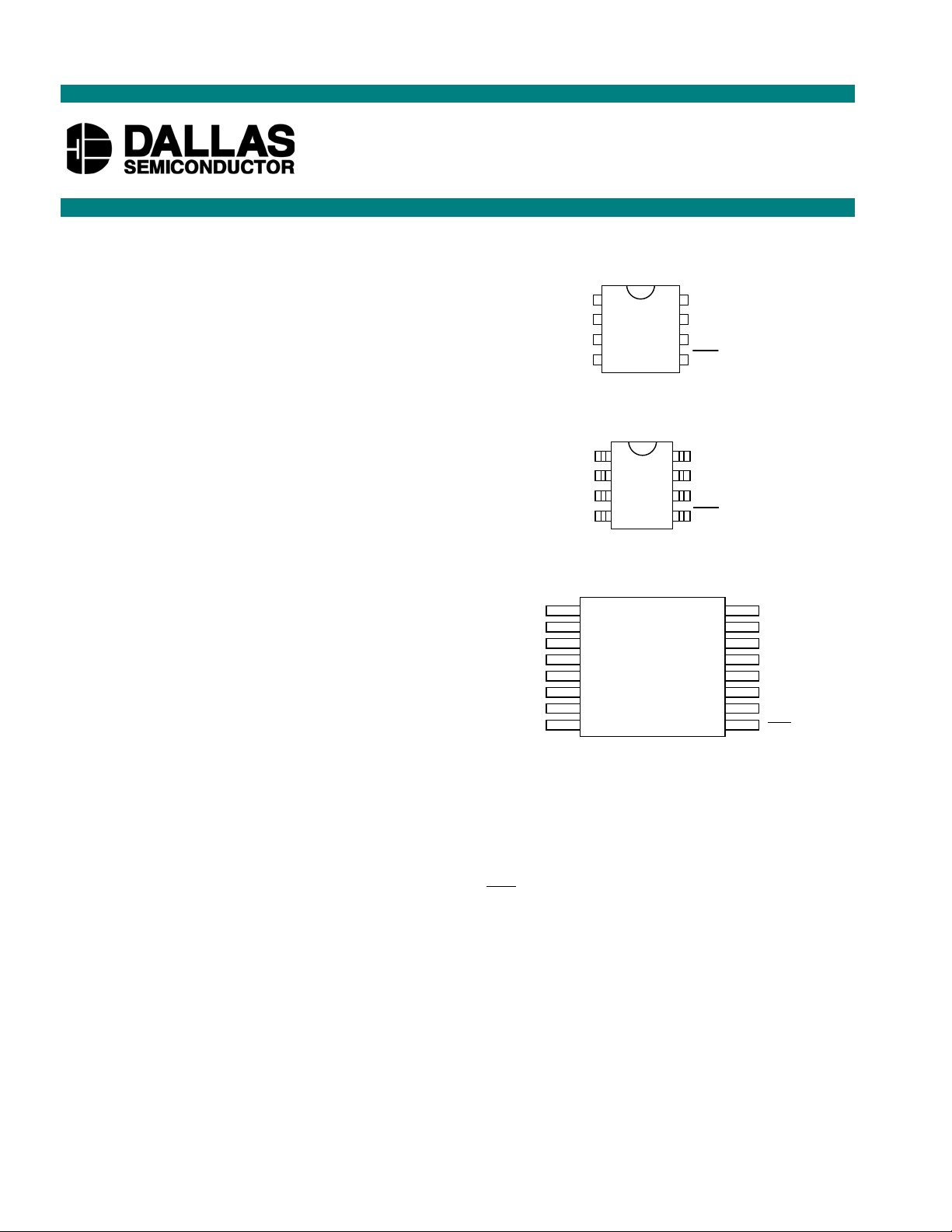
ORDERING INFORMATION
DS1302 8-Pin DIP (300-mil)
DS1302N 8-Pin DIP (Industrial)
DS1302S 8-Pin SOIC (200-mil)
DS1302SN 8-Pin SOIC (Industrial)
DS1302Z 8-Pin SOIC (150-mil)
DS1302ZN 8-Pin SOIC (Industrial)
DS1302S-16 16-Pin SOIC (300-mil)
DS1302SN-16 16-Pin SOIC (Industrial)
PIN ASSIGNMENT
V
GND
CC2
X1
X2
1
2
3
4
DS1302 8-Pin DIP (300-mil)
CC2
X1
X2
1
2
3
4
V
GND
DS1302 8-Pin SOIC (200-mil)
DS1302 8-Pin SOIC (150-mil)
V
CC2
X1
N
X2
GND
1
2
4
5
6
8
DS1302 16-Pin SOIC (300-mil)
V
8
CC1
7
SCLK
I/O
6
RST
5
V
8
CC1
SCLK
7
I/O
6
RST
5
V
CC1
1
N
RST
PIN DESCRIPTION
X1, X2 - 32.768kHz Crystal Pins
GND - Ground
RST - Reset
I/O - Data Input/Output
SCLK - Serial Clock
V
CC1
, V
CC2
- Power Supply Pins
DESCRIPTION
The DS1302 Trickle Charge Timekeeping Chip contains an RTC/calendar and 31 bytes of static RAM. It
communicates with a microprocessor via a simple serial interface. The RTC/calendar provides seconds,
minutes, hours, day, date, month, and year information. The end of the month date is automatically
adjusted for months with fewer than 31 days, including corrections for leap year. The clock operates in
either the 24-hour or 12-hour format with an AM/PM indicator.
1 of 15 092801
Page 2
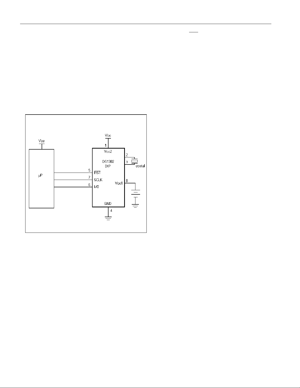
DS1302
Interfacing the DS1302 with a microprocessor is simplified by using synchronous serial communication.
Only three wires are required to communicate with the clock/RAM: 1) RST (reset), 2) I/O (data line), and
3) SCLK (serial clock). Data can be transferred to and from the clock/RAM 1 byte at a time or in a burst
of up to 31 bytes. The DS1302 is designed to operate on very low power and retain data and clock
information on less than 1 microwatt.
The DS1302 is the successor to the DS1202. In addition to the basic timekeeping functions of the
DS1202, the DS1302 has the additional features of dual-power pins for primary and back-up power
supplies, programmable trickle charger for V
, and seven additional bytes of scratchpad memory.
CC1
TYPICAL OPERATING CIRCUIT
2 of 15
Page 3
DS1302
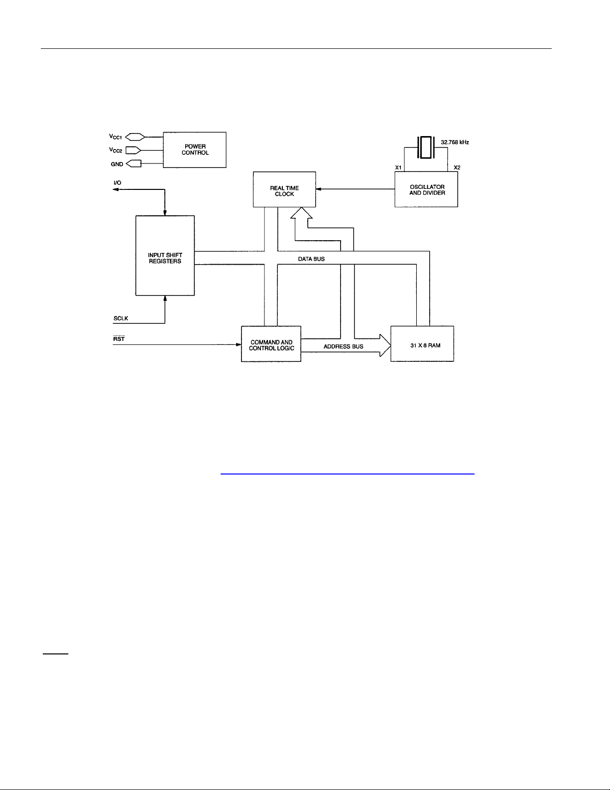
OPERATION
The main elements of the serial timekeeper (i.e., shift register, control logic, oscillator, RTC, and RAM)
are shown in Figure 1.
DS1302 BLOCK DIAGRAM Figure 1
SIGNAL DESCRIPTIONS
V
– V
CC1
power battery backup. In systems using the trickle charger, the rechargeable energy source is connected
to this pin. UL recognized to ensure against reverse charging current when used in conjunction with a
lithium battery.
See “Conditions of Acceptability” at http://www.maxim-ic.com/TechSupport/QA/ntrl.htm.
V
– V
CC2
backup source to maintain the time and date in the absence of primary power.
The DS1302 will operate from the larger of V
will power the DS1302. When V
SCLK (Serial Clock Input) – SCLK is used to synchronize data movement on the serial interface. This
pin has a 40kΩ internal pull-down resistor.
I/O (Data Input/Output) – The I/O pin is the bi-directional data pin for the 3-wire interface. This pin has
a 40kΩ internal pull-down resistor.
RST (Reset) – The reset signal must be asserted high during a read or a write. This pin has a 40kΩ
internal pull-down resistor.
provides low-power operation in single supply and battery-operated systems as well as low-
CC1
is the primary power supply pin in a dual-supply configuration. V
CC2
is less than V
CC2
CC1
or V
CC1
. When V
CC2
, V
will power the DS1302.
CC1
CC2
is greater than V
is connected to a
CC1
+ 0.2V, V
CC1
CC2
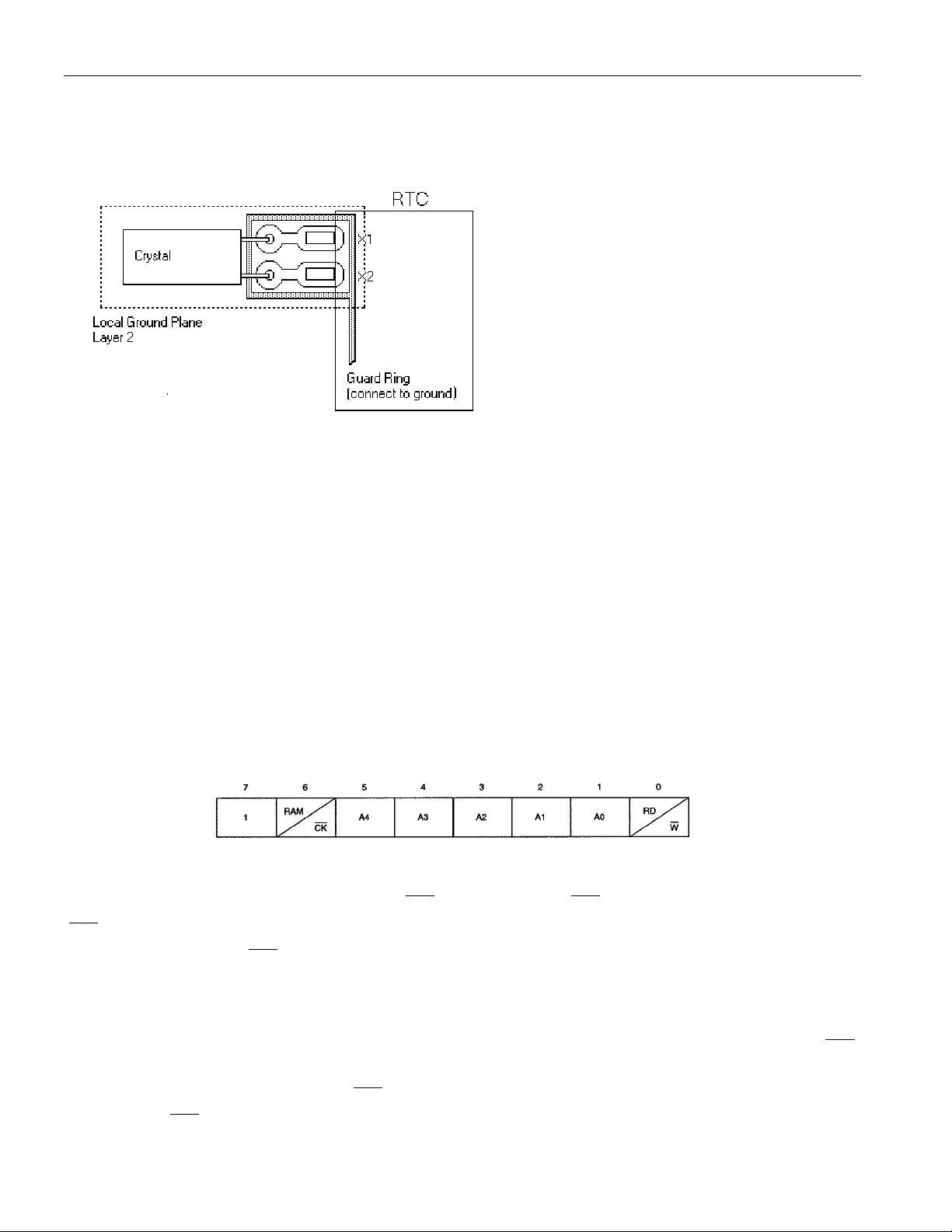
X1, X2 – Connections for a standard 32.768kHz quartz crystal. The internal oscillator is designed for
operation with a crystal having a specified load capacitance of 6pF. For more information on crystal
selection and crystal layout considerations, please consult Application Note 58, “Crystal Considerations
3 of 15
Page 4
DS1302
CO
OU
with Dallas Real-Time Clocks.” The DS1302 can also be driven by an external 32.768kHz oscillator. In
this configuration, the X1 pin is connected to the external oscillator signal and the X2 pin is floated.
RE
MMENDED LAY
T FOR CRYSTAL
CLOCK ACCURACY
The accuracy of the clock is dependent upon the accuracy of the crystal and the accuracy of the match
between the capactive load of the oscillator circuit and the capacitive load for which the crystal was
trimmed. Additional error will be added by crystal frequency drift caused by temperature shifts. External
circuit noise coupled into the oscillator circuit may result in the clock running fast. See Application Note
58, “Crystal Considerations with Dallas Real-Time Clocks” for detailed information.
COMMAND BYTE
The command byte is shown in Figure 2. Each data transfer is initiated by a command byte. The MSB
(Bit 7) must be a logic 1. If it is 0, writes to the DS1302 will be disabled. Bit 6 specifies clock/calendar
data if logic 0 or RAM data if logic 1. Bits 1 through 5 specify the designated registers to be input or
output, and the LSB (bit 0) specifies a write operation (input) if logic 0 or read operation (output) if logic
1. The command byte is always input starting with the LSB (bit 0).
ADDRESS/COMMAND BYTE Figure 2
RESET AND CLOCK CONTROL
All data transfers are initiated by driving the RST input high. The RST input serves two functions. First,
RST turns on the control logic, which allows access to the shift register for the address/command
sequence. Second, the
data transfer.
A clock cycle is a sequence of a falling edge followed by a rising edge. For data inputs, data must be
valid during the rising edge of the clock and data bits are output on the falling edge of clock. If the
input is low all data transfer terminates and the I/O pin goes to a high impedance state. Data transfer is
illustrated in Figure 3. At power-up,
logic 0 when
RST is driven to a logic 1 state.
RST signal provides a method of terminating either single byte or multiple byte
RST
RST must be a logic 0 until V
4 of 15
> 2.0V. Also SCLK must be at a
CC
Page 5

DS1302
DATA INPUT
Following the eight SCLK cycles that input a write command byte, a data byte is input on the rising edge
of the next eight SCLK cycles. Additional SCLK cycles are ignored should they inadvertently occur.
Data is input starting with bit 0.
DATA OUTPUT
Following the eight SCLK cycles that input a read command byte, a data byte is output on the falling
edge of the next eight SCLK cycles. Note that the first data bit to be transmitted occurs on the first falling
edge after the last bit of the command byte is written. Additional SCLK cycles retransmit the data bytes
should they inadvertently occur so long as RST remains high. This operation permits continuous burst
mode read capability. Also, the I/O pin is tri-stated upon each rising edge of SCLK. Data is output
starting with bit 0.
BURST MODE
Burst mode may be specified for either the clock/calendar or the RAM registers by addressing location 31
decimal (address/command bits 1 through 5 = logic 1). As before, bit 6 specifies clock or RAM and bit 0
specifies read or write. There is no data storage capacity at locations 9 through 31 in the Clock/Calendar
Registers or location 31 in the RAM registers. Reads or writes in burst mode start with bit 0 of address 0.
When writing to the clock registers in the burst mode, the first eight registers must be written in order for
the data to be transferred. However, when writing to RAM in burst mode it is not necessary to write all
31 bytes for the data to transfer. Each byte that is written to will be transferred to RAM regardless of
whether all 31 bytes are written or not.
CLOCK/CALENDAR
The clock/calendar is contained in seven write/read registers as shown in Figure 4. Data contained in the
clock/ calendar registers is in binary coded decimal format (BCD).
CLOCK HALT FLAG
Bit 7 of the seconds register is defined as the clock halt flag. When this bit is set to logic 1, the clock
oscillator is stopped and the DS1302 is placed into a low-power standby mode with a current drain of less
than 100 nanoamps. When this bit is written to logic 0, the clock will start. The initial power on state is
not defined.
AM-PM/12-24 MODE
Bit 7 of the hours register is defined as the 12- or 24-hour mode select bit. When high, the 12-hour mode
is selected. In the 12-hour mode, bit 5 is the AM/PM bit with logic high being PM. In the 24-hour mode,
bit 5 is the second 10-hour bit (20–23 hours).
WRITE PROTECT BIT
Bit 7 of the control register is the write-protect bit. The first seven bits (bits 0–6) are forced to 0 and will
always read a 0 when read. Before any write operation to the clock or RAM, bit 7 must be 0. When high,
the write protect bit prevents a write operation to any other register. The initial power on state is not
defined. Therefore the WP bit should be cleared before attempting to write to the device.
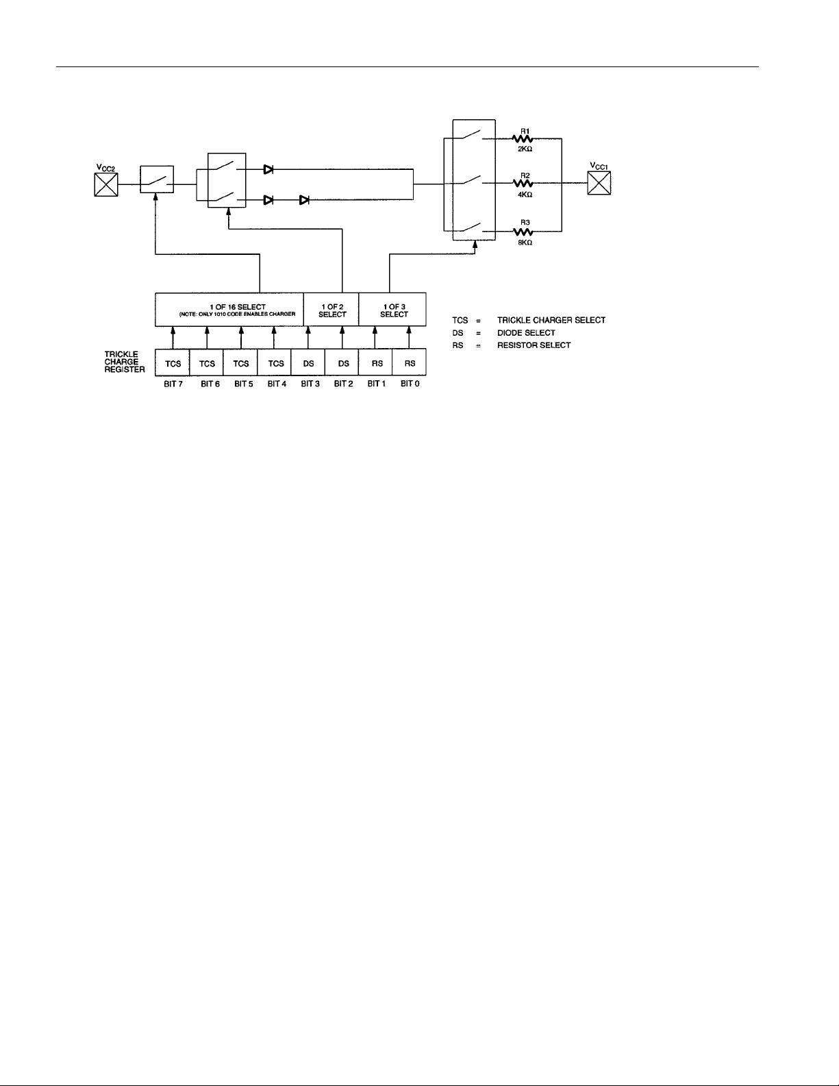
TRICKLE CHARGE REGISTER
This register controls the trickle charge characteristics of the DS1302. The simplified schematic of
Figure 5 shows the basic components of the trickle charger. The trickle charge select (TCS) bits
(bits 4–7) control the selection of the trickle charger. In order to prevent accidental enabling, only a
pattern of 1010 will enable the trickle charger. All other patterns will disable the trickle charger. The
5 of 15
Page 6
DS1302
DS1302 powers up with the trickle charger disabled. The diode select (DS) bits (bits 2–3) select whether
one diode or two diodes are connected between V
CC2
and V
. If DS is 01, one diode is selected or if DS
CC1
is 10, two diodes are selected. If DS is 00 or 11, the trickle charger is disabled independently of TCS.
The RS bits (bits 0–1) select the resistor that is connected between V
CC2
and V
. The resistor selected
CC1
by the resistor select (RS) bits is as follows:
RS Bits Resistor Typical Value
00 None None
01 R1 2kΩ
10 R2 4kΩ
11 R3 8kΩ
If RS is 00, the trickle charger is disabled independently of TCS.
Diode and resistor selection is determined by the user according to the maximum current desired for
battery or super cap charging. The maximum charging current can be calculated as illustrated in the
following example. Assume that a system power supply of 5V is applied to V
connected to V
between V
CC2
. Also assume that the trickle charger has been enabled with one diode and resistor R1
CC1
and V
. The maximum current I
CC1
I
= (5.0V - diode drop)/R1 » (5.0V - 0.7V) / 2kΩ » 2.2mA
MAX
would, therefore, be calculated as follows:
MAX
and a super cap is
CC2
As the super cap charges, the voltage drop between V
CC1
and V
will decrease and, therefore, the
CC2
charge current will decrease.
CLOCK/CALENDAR BURST MODE
The clock/calendar command byte specifies burst mode operation. In this mode the first eight
clock/calendar registers can be consecutively read or written (See Figure 4) starting with bit 0 of address
0.
If the write protect bit is set high when a write clock/calendar burst mode is specified, no data transfer
will occur to any of the eight clock/calendar registers (this includes the control register). The trickle
charger is not accessible in burst mode.
At the beginning of a clock burst read, the current time is transferred to a second set of registers. The
time information is read from these secondary registers, while the clock may continue to run. This
eliminates the need to re-read the registers in case of an update of the main registers during a read.
RAM
The static RAM is 31 x 8 bytes addressed consecutively in the RAM address space.
RAM BURST MODE
The RAM command byte specifies burst mode operation. In this mode, the 31 RAM registers can be
consecutively read or written (See Figure 4) starting with bit 0 of address 0.
REGISTER SUMMARY
A register data format summary is shown in Figure 4.
6 of 15
Page 7
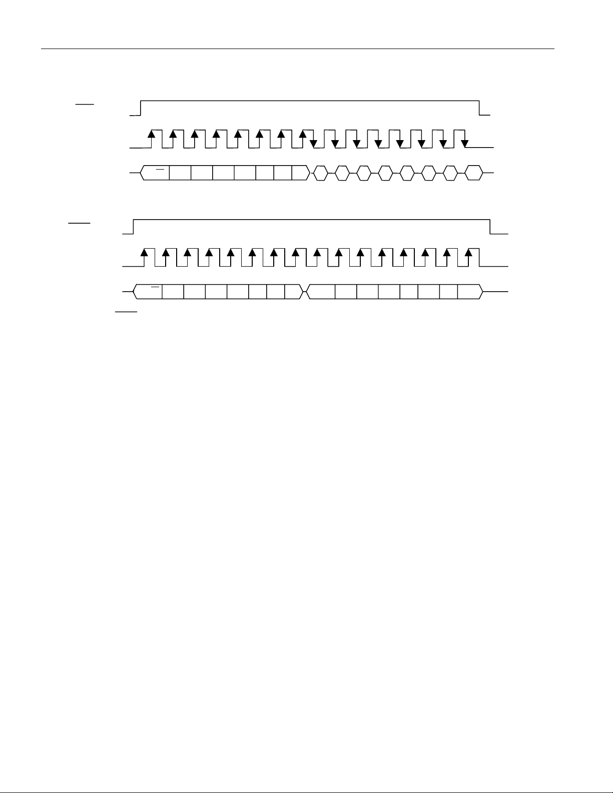
DATA TRANSFER SUMMARY Figure 3
SINGLE BYTE READ
RST
SCLK
DS1302
I/O
SINGLE BYTE WRITE
RST
SCLK
I/O
R/ W A0 A1 A2 A3 A4 R/C 1
R/ W A0 A1 A2 A3 A4 R/C 1
In burst mode, RST is kept high and additional SCLK cycles are sent until the end of the burst.
7 of 15
Page 8

REGISTER ADDRESS/DEFINITION Figure 4
DS1302
8 of 15
Page 9
DS1302 PROGRAMMABLE TRICKLE CHARGER Figure 5
DS1302
9 of 15
Page 10

DS1302
ABSOLUTE MAXIMUM RATINGS*
Voltage on Any Pin Relative to Ground -0.5V to +7.0V
Storage Temperature -55°C to +125°C
Soldering Temperature 260°C for 10 seconds (DIP)
See IPC/JEDEC Standard J-STD-020A for
Surface Mount Devices
* This is a stress rating only and functional operation of the device at these or any other conditions above
those indicated in the operation sections of this specification is not implied. Exposure to absolute
maximum rating conditions for extended periods of time may affect reliability.
Range Temperature V
Commercial 0°C to 70°C 2.0V to 5.5V V
Industrial -40°C to +85°C 2.0V to 5.5V V
CC
CC1
CC1
or V
or V
CC2
CC2
RECOMMENDED DC OPERATING CONDITIONS
(Over the operating range*)
PARAMETER SYMBOL MIN TYP MAX UNITS NOTES
Supply Voltage V
CC1
, V
CC2
V
V
Logic 1 Input V
CC1,
CC2
IH
2.0 5.5 V 8
2.0 VCC +
V
0.3
Logic 0 Input V
VCC = 2.0V -0.3 +0.3
IL
VCC = 5V –0.3 +0.8
V
*Unless otherwise specified.
DC ELECTRICAL CHARACTERISTICS
(Over the operating range*)
PARAMETER SYMBOL MIN TYP MAX UNITS NOTES
Input Leakage I
I/O Leakage I
Logic 1 Output IOH = -0.4mA
I
= -1.0mA
OH
Logic 0 Output IOL = 1.5mA
I
= 4.0mA
OL
V
V
Active Supply Current I
Timekeeping Current (OSC On) I
Standby Current (OSC Off) I
Active Supply Current I
Timekeeping Current (OSC On) I
Standby Current (OSC Off) I
LI
LO
OH
OL
CC1A
CC1T
CC1S
CC2A
CC2T
CC2S
VCC = 2.0V 1.6
VCC = 5V 2.4
VCC = 2.0V 0.4
VCC = 5V 0.4
V
= 2.0V 0.4
CC1
V
= 5V 1.2
CC1
V
= 2.0V 0.3
CC1
V
= 5V 1
CC1
V
= 2.0V 100
CC1
V
= 5V 100
CC1
IND 200
V
= 2.0V 0.425
CC2
V
= 5V 1.28
CC2
V
= 2.0V 25.3
CC2
V
= 5V 81
CC2
V
= 2.0V 25
CC2
V
= 5V 80
CC2
+500 mA3
+500 mA3
V
V
mA 2,9
mA 1,9
nA 7,9,11
mA 2,10
mA 1,10
mA 7,10
10 of 15
Page 11

Trickle Charge Resistors
Trickle Charge Diode Voltage Drop V
*Unless otherwise specified.
R1
R2
R3
TD
2
4
8
kΩ
kΩ
kΩ
0.7 V
DS1302
CAPACITANCE (T
= 25ºC)
A
PARAMETER SYMBOL MIN TYP MAX UNITS NOTES
Input Capacitance C
I/O Capacitance C
Crystal Capacitance C
I
I/O
X
10 pF
15 pF
6pF
AC ELECTRICAL CHARACTERISTICS
(Over the operating range*)
PARAMETER SYMBOL MIN TYP MAX UNITS NOTES
Data to CLK Setup t
CLK to Data Hold t
CLK to Data Delay t
CLK Low Time t
CLK High Time t
CLK Frequency t
DC
CDH
CDD
CL
CH
CLK
CLK Rise and Fall tR, t
RST to CLK Setup
CLK to RST Hold
RST Inactive Time
RST to I/O High-Z
SCLK to I/O High-Z t
t
CC
t
CCH
t
CWH
t
CDZ
CCZ
*Unless otherwise specified.
VCC = 2.0V 200
VCC = 5V 50
VCC = 2.0V 280
VCC = 5V 70
VCC = 2.0V 800
VCC = 5V 200
VCC = 2.0V 1000
VCC = 5V 250
VCC = 2.0V 1000
VCC = 5V 250
VCC = 2.0V 0.5
VCC = 5V DC 2.0
VCC = 2.0V 2000
F
VCC = 5V 500
VCC = 2.0V 4
VCC = 5V 1
VCC = 2.0V 240
VCC = 5V 60
VCC = 2.0V 4
VCC = 5V 1
VCC = 2.0V 280
VCC = 5V 70
VCC = 2.0V 280
VCC = 5V 70
ns 4
ns 4
ns 4,5,6
ns 4
ns 4
MHz 4
ns 4
ms
ns 4
ms
ns 4
ns 4
4
4
11 of 15
Page 12

TIMING DIAGRAM: READ DATA TRANSFER Figure 5
TIMING DIAGRAM: WRITE DATA TRANSFER Figure 6
DS1302
NOTES:
1. I
2. I
3. RST , SCLK, and I/O all have 40kΩ pull-down resistors to ground.
4. Measured at V
5. Measured at VOH = 2.4V or VOL = 0.4V.
6. Load capacitance = 50pF.
7. I
8. V
9. V
10. V
11. Typical values are at 25°C.
CC1T
and I
are specified with I/O open, RST set to a logic 0, and clock halt flag = 0 (oscillator
CC2T
enabled).
CC1A
and I
are specified with the I/O pin open, RST high, SCLK=2MHz at VCC = 5V;
CC2A
SCLK = 500kHz, VCC = 2.0V, and clock halt flag = 0 (oscillator enabled).
= 2.0V or VIL = 0.8V and 10ns maximum rise and fall time.
IH
CC1S
and I
are specified with RST , I/O, and SCLK open. The clock halt flag must be set to logic
CC2S
one (oscillator disabled).
CC
CC2
CC1
= V
= 0V.
= 0V.
, when V
CC2
CC2
> V
+ 0.2V; VCC = V
CC1
, when V
CC1
CC1
> V
CC2
.
12 of 15
Page 13
DS1302 SERIAL TIMEKEEPER 8-PIN DIP (300-MIL)
PKG 8-PIN
DIM MIN MAX
A IN.
MM
B IN.
MM
C IN.
MM
D IN.
MM
E IN.
MM
F IN.
MM
G IN.
MM
H IN.
MM
J IN.
MM
K IN.
MM
0.360
9.14
0.240
6.10
0.120
3.05
0.300
7.62
0.015
0.38
0.120
3.04
0.090
2.29
0.320
8.13
0.008
0.20
0.015
0.38
DS1302
0.400
10.16
0.260
6.60
0.140
3.56
0.325
8.26
0.040
1.02
0.140
3.56
0.110
2.79
0.370
9.40
0.012
0.30
0.021
0.53
13 of 15
Page 14

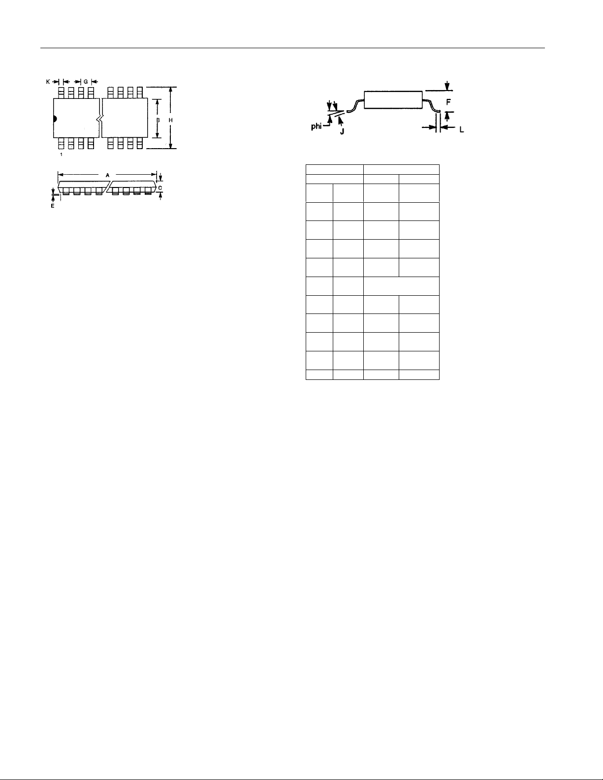
DS1302S SERIAL TIMEKEEPER 8-PIN SOIC (150-MIL AND 200-MIL)
DS1302
PKG 8-PIN
DIM MIN MAX MIN MAX
A IN.
MM
B IN.
MM
C IN.
MM
E IN.
MM
F IN.
MM
G IN.
MM
H IN.
MM
J IN.
MM
K IN.
MM
L IN.
MM
phi
(150-MIL)
0.188
4.78
0.150
3.81
0.048
1.22
0.004
0.10
0.053
1.35
0.230
5.84
0.007
0.18
0.012
0.30
0.016
0.41
0° 8° 0° 8°
0.196
4.98
0.158
4.01
0.062
1.57
0.010
0.25
0.069
1.75
0.050 BSC
1.27 BSC
0.244
6.20
0.011
0.28
0.020
0.51
0.050
1.27
8-PIN
(200-MIL)
0.203
5.16
0.203
5.16
0.070
1.78
0.004
0.10
0.074
1.88
0.302
7.67
0.006
0.15
0.013
0.33
0.019
0.48
0.213
5.41
0.213
5.41
0.074
1.88
0.010
0.25
0.084
2.13
0.318
8.08
0.010
0.25
0.020
0.51
0.030
0.76
14 of 15
Page 15
DS1302S SERIAL TIMEKEEPER 16-PIN SOIC
A
B
C
E
F
G
H
J
K
L
phi
PKG 16-PIN
DIM MIN MAX
IN
MM
IN
MM
IN
MM
IN
MM
IN
MM
IN
MM
IN
MM
IN
MM
IN
MM
IN
MM
0.398
10.11
0.290
7.37
0.089
2.26
0.004
0.102
0.004
2.39
0.050 BSC
1.27 BSC
0.398
10.11
0.009
0.229
0.013
0.33
0.016
0.40
0° 8°
0.412
10.46
0.300
7.62
0.095
2.41
0.012
0.30
0.105
2.67
0.416
10.57
0.013
0.33
0.020
0.51
0.040
1.02
DS1302
15 of 15
 Loading...