

Page 1
A
www.maxim-ic.com
A
DS12C887
Real-Time Clock
FEATURES
§ Drop-in replacement for IBM AT computer
clock/calendar
§ Pin compatible with the MC146818B and
DS1287A
§ Totally nonvolatile with over 10 years of
operation in the absence of power
§ Self-contained subsystem includes lithium,
quartz, and support circuitry
§ Counts seconds, minutes, hours, days, day of
the week, date, month, and year with leapyear compensation valid up to 2100
§ Binary or BCD representation of time,
calendar, and alarm
§ 12- or 24-hour clock with AM and PM in 12-
hour mode
§ Daylight Savings Time option
§ Selectable between Motorola and Intel bus
timing
§ Multiplex bus for pin efficiency
§ Interfaced with software as 128 RAM
locations
– 15 bytes of clock and control registers
– 113 bytes of general purpose RAM
§ Programmable square-wave output signal
§ Bus-compatible interrupt signals (IRQ)
§ Three interrupts are separately software-
maskable and testable
– Time-of-day alarm once/second to
once/day
– Periodic rates from 122ms to 500ms
– En-of-clock update cycle
§ Century register
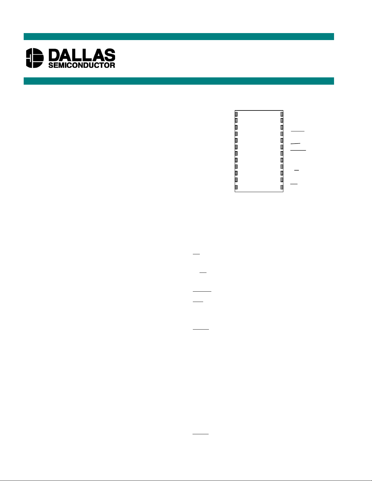
PIN ASSIGNMENT
MOT
NC
NC
AD0
AD1
AD2
AD3
AD4
AD5
AD6
AD7
GND
24-Pin Encapsulated Package
1
2
3
4
5
6
7
8
9
10
11
12
DS12C887A
24
23
22
21
20
19
18
17
16
15
14
13
V
CC
SQW
NC
RCLR
NC
IRQ
RESET
DS
NC
R/W
S
CS
PIN DESCRIPTION
AD0–AD7 - Multiplexed Address/Data Bus
NC - No Connect
MOT - Bus Type Selection
CS - RTC Chip Select Input
AS - Address Strobe
R/ W - Read/Write Input
DS - Data Strobe
RESET - Reset Input
IRQ - Interrupt Request Output
SQW - Square-Wave Output
V
CC
RCLR - RAM Clear
GND - Ground
- +5V Main Supply
DESCRIPTION
The DS12C887A real-time clock plus RAM is designed to be a direct upgrade replacement for the
DS12887A in existing IBM-compatible personal computers to add hardware year-2000 compliance. A
century byte was added to memory location 50, 32h, as called out by the PC AT specification. The
DS12C887A is identical in form, fit, and function to the DS1287A, and provides additional 64 bytes of
general-purpose RAM. Access to this additional RAM space is determined by the logic level presented on
AD6 during the address portion of an access cycle. The
bytes of general purpose RAM but does not affect the RAM associated with the real time clock. In order
RCLR pin is used to clear (set to logic 1) all 113
1 of 2 111901
Page 2
DS12C887A
to clear the RAM, RCLR must be forced to an input logic 0 (-0.3V to +0.8V) during battery-backup mode
when V
is not applied. The RCLR function is designed to be used via human interface (shorting to
CC
ground manually or by switch) and not to be driven with external buffers.
For a complete description of operating conditions, electrical characteristics, bus timing and pin
descriptions other than
RCLR , see the DS12C887 data sheet.
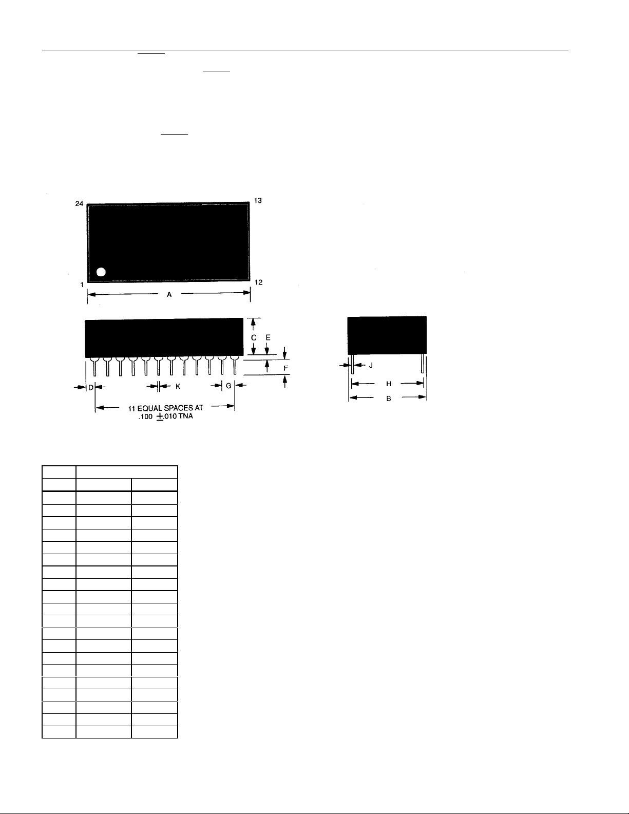
DS12C887 REAL-TIME CLOCK PLUS RAM
PKG 24-PIN
DIM MIN MAX
A IN.
MM
B IN.
MM
C IN.
MM
D IN.
MM
E IN.
MM
F IN.
MM
G IN.
MM
H IN.
MM
J IN.
MM
K IN.
MM
1.320 1.335
33.53 33.91
0.675 0.700
17.15 17.78
0.345 0.370
8.76 9.40
0.100 0.130
2.54 3.30
0.015 0.030
0.38 0.76
0.110 0.140
2.79 3.56
0.090 0.110
2.29 2.79
0.590 0.630
14.99 16.00
0.008 0.012
0.20 0.30
0.015 0.021
0.38 0.53
.
Note: Pins 2, 3, 16, 20, and 22 are missing by design.
This device cannot be stored or shipped in conductive
material that will give a continuity path between the RAM
clear pin and ground.
2 of 2
 Loading...