

Page 1

r
www.dalsemi.com
(
)
DS1286
Watchdog Timekeepe
FEATURES
Keeps track of hundredths of seconds,
seconds, minutes, hours, days, date of the
month, months, and years; valid leap year
compensation up to 2100
Watchdog timer restarts an out-of-control
processor
Alarm function schedules real time-related
activities
Embedded lithium energy cell maintains time,
watchdog, user RAM, and alarm information
Programmable interrupts and square wave
outputs maintain 28-pin JEDEC footprint
All registers are individually addressable via
the address and data bus
Accuracy is better than ±1 minute/month at
25°C
Greater than 10 years of timekeeping in the
absence of V
50 bytes of user NV RAM
CC
PIN ASSIGNMENT
V
INTA
NC
NC
NC
A5
A4
A3
A2
A1
A0
DQ0
DQ1
DQ2
GND
1
2
3
4
5
6
7
8
9
10
11
12
13
14
28
27
26
25
24
23
22
21
20
19
18
17
16
15
CC
WE
INTB
NC
NC
SQW
OE
NC
CE
DQ7
DQ6
DQ5
DQ4
DQ3
INTB
28-Pin Encapsulated Package
(720-Mil Flush)
PIN DESCRIPTION
INTA - Interrupt Output A (open drain)
INTB (INTB) - Interrupt Output B (open drain)
A0-A5 - Address Inputs
DQ0-DQ7 - Data Input/Output
CE - Chip Enable
OE - Output Enable
WE - Write Enable
V
- +5 Volts
CC
GND - Ground
NC - No Connection
SQW - Square Wave Output
DESCRIPTION
The DS1286 Watchdog Timekeeper is a self-contained real time clock, alarm, watchdog timer, and
interval timer in a 28-pin JEDEC DIP package. The DS1286 contains an embedded lithium energ y source
and a quartz crystal which eliminates the need for any external circuitry. Data contained within 64 eightbit registers can be read or written in the same manner as bytewide static RAM. Data is maintained in the
Watchdog Timekeeper by intelligent control circuitry which detects the status of V
memory when V
10 years in the absence of V
is out of tolerance. The lithium energy source can maintain data and real time for over
CC
. Watchdog Timekeeper information includes hundredths of seconds,
CC
seconds, minutes, hours, day, date, month, and year. The date at the end of the month is automatically
1 of 13 111999
and write protects
CC
Page 2

DS1286
adjusted for months with less than 31 days, including correction for leap year. The Watchdog Timekeeper
operates in either 24-hour or 12-hour format with an AM/PM indicator. The watchdog timer provides
alarm windows and interval timing between 0.01 seconds and 99.99 seconds. The real time alarm
provides for preset times of up to one week.
OPERATION - READ REGISTERS
The DS1286 executes a read cycle whenever WE (Write Enable) is inactive (High) and CE (Chip
Enable) and OE (Output Enable) are active (Low). The unique address specified by the six address inputs
(A0-A5) defines which of the 64 registers is to be accessed. Valid data will be available to the eight data
output drivers within t
and OE access times are also satisfied. If OE and CE access times are not satisfied, then data access must
(Access Time) after the last address input signal is stable, providing that CE
ACC
be measured from the latter occu rring signal (CE or OE ) and the limiting parameter is either t
or t
for OE rather than address access.
OE
for CE
CO
OPERATION - WRITE REGISTERS
The DS1286 is in the write mode whenever the WE (Write Enable) and CE (Chip Enable) signals are i n
the active (Low) state after the address inputs are stable. The latter o ccurring falling edge of CE or WE
will determine the start of the write cycle. The write cycle is terminated by the earlier rising edge of CE
or WE . All address inputs must be kept valid throughout the write cycle. WE must return to the high state
for a minimum recovery state (tWR) before another cycle can be initiated. Data must be valid on the data
bus with sufficient Data Set Up (tDS) and Data Hold Time (tDH) with respect to the earlier rising edge of
CE or WE . The OE control signal should be kept inactive (High) during write cycles to avoid bus
contention. However, if the output bus has been enabled (CE and OE active), then WE will disable the
outputs in t
from its falling edge.
ODW
DATA RETENTION
The Watchdog Timekeeper provides full functional capability when V
write protects the register contents at 4.25 volts typical. Data is maintained in the absence of V
any additional support circuitry. The DS1286 constantly monitors V
CC
the Watchdog Timekeeper will automatically write protect itself and all inputs to the registers become
“Don’t Care.” Both INTA and INTB (INTB) are open drain outputs. The two interrupts and the internal
clock continue to run regardless of the level of VCC. However, it is important to insure that the pull-up
resistors used with the interrupt pins are never pulled up to a value which is greater than V
V
falls below approximately 3.0 volts, a power switching circuit turns on the lithium energy source to
CC
maintain the clock, and timer data functionality. It is also required to insure that during this time (battery
is greater than 4.5 volts and
CC
without
CC
. Should the supply voltage decay,
+ 0.3V. As
CC
backup mode), the voltage present at
INTA and INTB (INTB) never exceeds 3.0V. At all times the
current on each should not exceed +2.1 mA or -1.0 mA. However, if the active hi gh mode is selected for
INTB (INTB), this pin will only go high in the presence of V
approximately 3.0 volts, the power switching circuit connects external V
lithium energy source. Normal operation can resume after V
. During power-up, when V
CC
and disconnects the internal
CC
exceeds 4.5 volts for a period of 150 ms.
CC
rises above
CC
2 of 13
Page 3

DS1286
WATCHDOG TIMEKEEPER REGISTERS
The Watchdog Timekeeper has 64 registers which are 8 bits wide that contain all of the Timekeeping,
Alarm, Watchdog, Control, and Data information. The Clock, Calendar, Alarm, and Watchdog registers
are memory locations which contain external (user-accessible) and internal copies of the data. The
external copies are independent of internal functions except that they are updated periodically by the
simultaneous transfer of the incremented internal copy (see Figure 1). The Command Register bits are
affected by both internal and external functions. This register will be discussed later. The 50 bytes of
RAM registers can only be accessed from the external address and data bus. Registers 0, 1, 2, 4, 6, 8, 9,
and A contain time of day and date information (see Figure 2). Time of Day information is stored in
BCD. Registers 3, 5, and 7 contain the Time of Day Alarm information. Time of Da y Alarm information
is stored in BCD. Register B is the Command Register and information in this register is binary. Registers
C and D are the Watchdog Alarm registers and information which is stored in these two registers is in
BCD. Registers E through 3F are user bytes and can be used to contain data at the user’s discretion.
3 of 13
Page 4
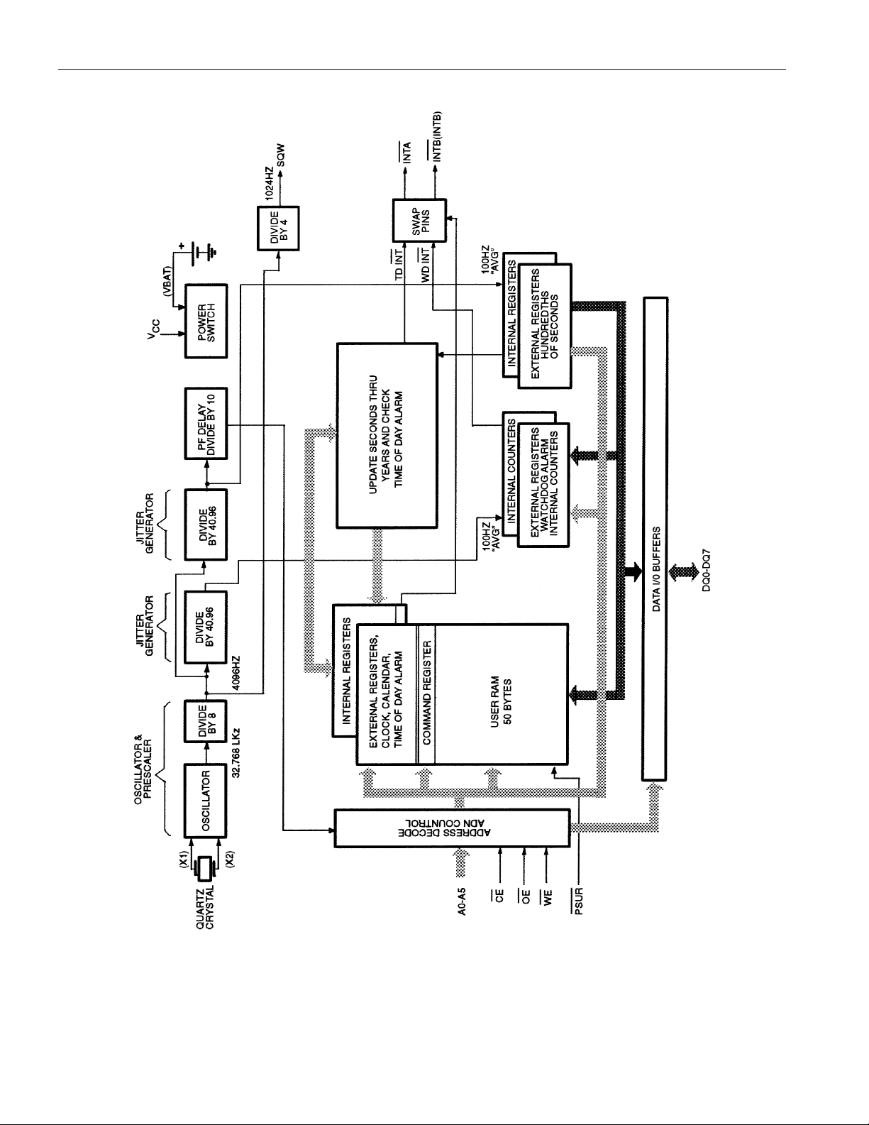
BLOCK DIAGRAM Figure 1
DS1286
4 of 13
Page 5

DS1286 WATCHDOG TIMEKEEPER REGISTERS Figure 2
DS1286
5 of 13
Page 6

DS1286
TIME OF DAY REGISTERS
Registers 0, 1, 2, 4, 6, 8, 9, and A contain Time of Day data in BCD. Ten bits within these eight registers
are not used and will always read 0 regardless of how they are written. Bits 6 and 7 in the Months
Register (9) are binary bits. When set to logic 0, EOSC (bit 7) enables the Real Time Clock oscillator.
This bit is set to logic 1 as shipped from Dallas Semiconductor to prevent lithium energy consumption
during storage and shipment. This bit will normally be turned on by the user during device initialization.
However, the oscillator can be turned on and off as necessary by setting this bit to the appropriate level.
Bit 6 of this same byte controls the Square Wave Output (Pin 23). When set to logic 0, the Square Wave
Output pin will output a 1024 Hz Square Wave Signal. When set to logic 1 the Square Wave Output pin
is in a high impedance state. Bit 6 of the Hours Register is defined as the 12- or 24- hour Select Bit. When
set to logic 1, the 12-hour format is selected. In the 12-hour format, bit 5 is the AM/PM bit with logic 1
being PM. In the 24-hour mode, bit 5 is the second 10-hour bit (20-23 hours). The Time of Day registers
are updated every .01 seconds from the real time clock, except when the TE bit (bit 7 of Register B) is set
low or the clock oscillator is not running. The preferred method of synchronizing data acc ess to and from
the Watchdog Timekeeper is to access the Command Register by doing a write cycle to address location
0B and setting the TE bit (Transfer Enable ) to a logic 0. This will freeze the External Time of Day
registers at the present recorded time, allowing access to occur without dan ger of simultaneous update.
When the watch registers have been read or written, a second write cycle to location 0B, setting the TE
bit to a logic 1, will put the Time of Day registers back to being updated every 0.01 second. No time is
lost in the real time clock because the internal copy of the Time of Day register buffers is continually
incremented while the external memory registers are frozen.
An alternate method of reading and writing the Time of Day registers is to ignore synchronization.
However, any single read may give erroneous data as the real time clock may be in the process of
updating the external memory registers as data is being read. The internal copies of seconds through years
are incremented and Time of Day Alarm is checked during the period that hundreds of seconds re ad 99
and are transferred to the external register when hundredths of seconds roll from 99 to 00. A way of
making sure data is valid is to do multiple reads and compare. Writing the registers can also produce
erroneous results for the same reasons. A way of making sure that the write cycle has caused proper
update is to do read verifies and re-execute the write c ycle if data is not correct. While the possibility of
erroneous results from reads and write cycles has been stated, it is worth noting that the probability of an
incorrect result is kept to a minimum due to the redundant structure of the Watchdog Timekeeper.
TIME OF DAY ALARM REGISTERS
Registers 3, 5, and 7 contain the Time of Day Alarm registers. Bits 3, 4, 5, and 6 of Register 7 will
always read 0 regardless of how they are written. Bit 7 of Registers 3, 5, and 7 are mask bits (Figure 3).
When all of the mask bits are logic 0, a Time of Day Alarm will only occur when Registers 2, 4, and 6
match the values stored in Registers 3, 5, and 7. An alarm will be generated every day when bit 7 of
Register 7 is set to a logic 1. Similarly, an alarm is generated every hour when bit 7 of Registers 7 and 5
is set to a logic 1. When bit 7 of Registers 7, 5, and 3 is set to a logic 1, an alarm will occur every minute
when Register 1 (seconds) rolls from 59 to 00.
Time of Day Alarm registers are written and read in the same format as the Time of Day registers. The
Time of Day Alarm Flag and Interrupt is always cleared when Alarm registers are read or written.
6 of 13
Page 7

DS1286
WATCHDOG ALARM REGISTERS
Registers C and D contain the time for the Watchdog Alarm. The two registers contain a time count f rom
to 99.99 seconds in BCD. The value written into the Watchdog Alarm Registers can be written or read in
any order. Any access to Registers C or D will cause the Watchdog Alarm to reinitialize and clears the
Watchdog Flag bit and the Watchdog Interrupt Output. When a new value is ente red or the Watchdog
Registers are read, the Watchdog Timer will start counting down from the entered value to 0. When 0 is
reached, the Watchdog Interrupt Output will go to the active state. The Watchdog Timer countdown is
interrupted and reinitialized back to the entered value every time either of the re gisters is a ccess ed. In this
manner, controlled periodic accesses to the Watchdog Timer can prevent the Watchdog Alarm from ever
going to an active level. If access does not occur, countdown alarm will be repetitive. The Watchdog
Alarm registers always read the entered value. The actual countdown register is internal and is not
readable. Writing Registers C and D to 0 will disable the Watchdog Alarm feature.
COMMAND REGISTER
Address location 0B is the Command Register where mask bits, control bits, and flag bits reside. Bit 0 is
the Time of Day Alarm Flag (TDF). When this bit is set internally to a logic 1, an alarm has occurred.
The time of the alarm can be determined by reading the Time of Day Alarm registers. However, if the
transfer enable bit is set to logic 0 the Time of Day registers may not reflect the exact time that the alarm
occurred. This bit is read only and writing this register has no effect on the bit. The bit is reset when any
of the Time of Day Alarm registers are read. Bit 1 is the Watchdog Alarm Flag (WAF). When this bit is
set internally to a logic 1, a Watchdog Alarm has occurred. This bit is read only and writing this register
has no effect on the bit. The bit is reset wh en any of the Watchdo g Alarm r egisters a re accessed. Bit 2 of
the Command Register contains the Time of Day Alarm Mask Bit (TDM). When this bit is written to a
logic 1, the Time of Day Alarm Interrupt Output is deactivated regardless of the value of the Time of Day
Alarm Flag. When TDM is set to logic 0, the Time of Day Interrupt Output will go to the active state,
which is determined by bits 0, 4, 5, and 6 of the Command Register. Bit 3 of the Command Register
contains the Watchdog Alarm Mask bit (WAM). When this bit is written to a logic 1, the Watchdog
Interrupt Output is deactivated regardless of the value in the Watchdog Alarm registers. When WAM is
set to logic 0, the Watchdog Interrupt Output will go to the active state which is determined by bits 1, 4,
5, and 6 of the Command Register. These 4 bits define how Interrupt Output Pins INTA and INTB (INTB)
will be operated. Bit 4 of the Command Register determines whether both interrupts will output a pulse or
level when activated. If bit 4 is set to logic 1, the pulse mode is selected and
minimum of 3 ms and then release. Output
INTB (INTB) will either sink or source current for a minimum
INTA will sink current for a
of 3 ms depending on the level of bit 5. When bit 5 is set to logic 1, the B interrupt will source current.
When bit 5 is set to logic 0, the B interrupt will sink current. Bit 6 of the Command Register directs
which type of interrupt will be present on interrupt pins
INTA or INTB (INTB). When set to logic 1, INTA
becomes the Time of Day Alarm Interrupt pin and INTB (INTB) becomes the Watchdog Interrupt pin.
When bit 6 is set to logic 0, the interrupt functions are reversed such that the Time of Day Alarm will be
output on INTB(INTB) and the Watchdog Interrupt will be output on INTA . Caution should be exercised
when dynamically setting this bit as the interrupts will be reversed even if in an active state. Bit 7 of the
Command Register is for Transfer Enable (TE). The function of this bit is described in the Time of Day
registers.
7 of 13
Page 8

DS1286
TIME OF DAY ALARM MASK BITS Figure 3
REGISTER
(3)MINUTES (5)HOURS (7)DAYS
1 1 1 ALARM ONCE PER MINUTE
0 1 1 ALARM WHEN MINUTES MATCH
0 0 1 ALARM WHEN HOURS AND MINUTES MATCH
0 0 0 ALARM WHEN HOURS, MINUTES, AND DAYS
MATCH
ABSOLUTE MAXIMUM RATINGS*
Voltage on Any Pin Relative to Ground -0.3V to +7.0V
Operating Temperature 0°C to 70°C
Storage Temperature -40°C to +70°C
Soldering Temperature 260°C for 10 seconds (See Note 14)
* This is a stress rating only and functional operation of the device at these or any other conditions
above those indicated in the operation sections of this specification is not implied. Exposure to
absolute maximum rating conditions for extended periods of time may affect reliability.
RECOMMENDED DC OPERATING CONDITIONS (0°C to 70°C)
PARAMETER SYMBOL MIN TYP MAX UNITS NOTES
Power Supply Voltage V
Input Logic 1 V
Input Logic 0 V
CC
IH
IL
4.5 5.0 5.5 V 10
2.2 VCC+0.3 V 10
-0.3 0.8 V 10
DC ELECTRICAL CHARACTERISTICS (0°C to 70°C; V
= 5V ±=10%)
CC
PARAMETER SYMBOL MIN TYP MAX UNITS NOTES
Input Leakage Current I
Output Leakage Current I
I/O Leakage Current
CE ≥ V
IH
≤ V
CC
Output Current @ 2.4V I
Output Current @ 0.4V I
Standby Current CE = 2.2V
Standby Current CE > VCC -0.5
Active Current I
Write Protection Voltage V
I
LIO
I
CCS1
I
CCS2
IL
LO
OH
OL
CC
TP
CAPACITANCE (t
-1.0 +1.0
-1.0 +1.0
-1.0 +1.0
µA
µA
µA
-1.0 mA
2.0 mA 13
3.0 7.0 mA
4.0 mA
15 mA
4.25 V
= 25°C)
A
PARAMETER SYMBOL MIN TYP MAX UNITS NOTES
Input Capacitance C
Output Capacitance C
Input/Output Capacitance C
IN
OUT
I/O
710pF
710pF
710pF
8 of 13
Page 9

DS1286
AC ELECTRICAL CHARACTERISTICS (0°C to 70°C; V
= 4.5V to 5.5V)
CC
PARAMETER SYMBOL MIN TYP MAX UNITS NOTES
Read Cycle Time t
Address Access Time t
CE Access Time
OE Access Time
OE or CE to Output Active
Output High Z from Deselect t
Output Hold from Address Change t
Write Cycle Time t
Write Pulse Width t
Address Setup Time t
Write Recovery Time t
Output High Z from WE
t
Output Active from WE
Data Setup Time t
Data Hold Time t
INTA , INTB Pulse Width
RC
ACC
t
CO
t
OE
t
COE
OD
OH
WC
WP
AW
WR
ODW
t
OEW
DS
DH
t
IPW
150 ns 1
150 ns
150 ns
60 ns
10 ns
60 ns
10 ns
150 ns
140 ns 3
0ns
10 ns
50 ns
10 ns
45 ns 4
0 ns 4,5
3 ns 11,12
READ CYCLE (NOTE 1)
WRITE CYCLE 1 ( No tes 2, 6, 7)
9 of 13
Page 10

WRITE CYCLE 2 ( N o tes 2, 8)
TIMING DIAGRAM: INTERRUPT
OUTPUTS PULSE MODE (SEE NOTES 11, 12)
DS1286
POWER
-DOWN/POWER-UP CONDITION
10 of 13
Page 11

DS1286
POWER-UP/POWER-DOWN CONDITION
PARAMETER SYMBOL MIN TYP MAX UNITS NOTES
CE at V
before Power-Down
IH
VCC slew from 4.5V to 0V (CE at VIH)
VCC slew from 0V to 4.5V (CE at VIH)
CE at V
after Power Up
IH
t
t
REC
PD
t
t
F
R
0
350
100
µs
µs
µs
150 ns
(tA=25°C)
PARAMETER SYMBOL MIN TYP MAX UNITS NOTES
Expected Data Retention Time t
DR
10 years 9
WARNING:
Under no circumstances are negative undershoots, of any amplitude, allowed when device is in battery
backup mode.
11 of 13
Page 12

DS1286
NOTES:
1. WE is high for a read cycle.
2. OE = VIH or VIL. If OE = V IH during write cycle, the output buffers remain in a high impedance
state.
3. tWP is specified as the logical A ND of the CE and WE . tWP is measured from the latter of CE or WE
going low to the earlier of CE or WE going high.
4. t
or tDH are measured from the earlier of CE or WE going high.
DS
5. tDH is measured from WE going high. If CE is used to terminate the write cycle, then tDH = 20 ns.
6. If the CE low transition occurs simultaneously with or later than the WE low transition in Write
Cycle 1, the output buffers remain in a high impedance state during this period.
7. If the CE high transition occurs prior to or simultaneously with the WE high transition, the output
buffers remain in a high impedance state during this period.
8. If
WE is low or the WE low transition occurs prior to or simultaneously with the CE low transition,
the output buffers remain in a high impedance state during this period.
9. Each DS1286 is marked with a four-digit date code AABB. AA designates the year of manufacture.
BB designates the week of manufacture. The expected t
is defined as starting at the date of
DR
manufacture.
10. All voltages are referenced to ground.
11. Applies to both interrupt pins when the alarms are set to pulse.
12. Interrupt output occurs within 100 ns on the alarm condition existing.
13. Both INTA and INTB(INTB) are open drain outputs.
14. Real-Time Clock Modules can be successfully processed through conventional wave-soldering
techniques as long as temperature exposure to the lithium energy source contained within does not
exceed +85°C. Post-solder cleaning with water washing techniques is acceptable, provided that
ultrasonic vibration is not used.
AC TEST CONDITIONS
Output Load: 100 pF + 1TTL Gate
Input Pulse Levels: 0-3.0V
Timing Measurement Reference Levels
Input: 1.5V
Output: 1.5V
Input Pulse Rise and Fall Times: 5 ns.
12 of 13
Page 13

DS1286 WATCHDOG TIMEKEEPER
N
PKG 28-PIN
DIM MIN MAX
A IN.
MM
B IN.
MM
C IN.
MM
D IN.
MM
E IN.
MM
F IN.
MM
G IN.
MM
H IN.
MM
J IN.
MM
K IN.
MM
1.520
38.61
0.695
17.65
0.350
8.89
0.100
2.54
0.015
0.38
0.110
2.79
0.090
2.29
0.590
14.99
0.008
0.20
0.015
0.38
1.540
39.12
0.720
18.29
0.375
9.52`
0.130
3.30
0.030
0.76
0.140
3.56
0.110
2.79
0.630
16.00
0.012
0.30
0.021
0.53
DS1286
OTE: PINS 2,3,21,24 AND 25 ARE MISSING BY
DESIGN
13 of 13
 Loading...