

Page 1
www.maxim-ic.com
A
A
A13A
A9A
A
A
A
A
A
A
A
A9A
A7A
A
A4A
A2A
A
A
DS1251/DS1251P
4096k NV SRAM with Phantom Clock
FEATURES
§ Real-time clock keeps track of hundredths of
seconds, minutes, hours, days, date of the
month, months, and years
§ 512k x 8 NV SRAM directly replaces
volatile static RAM or EEPROM
§ Embedded lithium energy cell maintains
calendar operation and retains RAM data
§ Watch function is transparent to RAM
operation
§ Month and year determine the number of
days in each month; valid up to 2100
§ Over 10 years of data retention in the
absence of power
§ Full 10% operating range
§ Lithium energy source is electrically
disconnected to retain freshness until power
is applied for the first time
§ DIP Module only
– Standard 32-pin JEDEC pinout
– Upward comparable with the DS1248
§ PowerCap® Module Board only
– Surface mountable package for direct
connection to PowerCap containing
battery and crystal
– Replaceable battery (PowerCap)
– Pin for pin compatible with other densities
of DS124XP phantom clocks
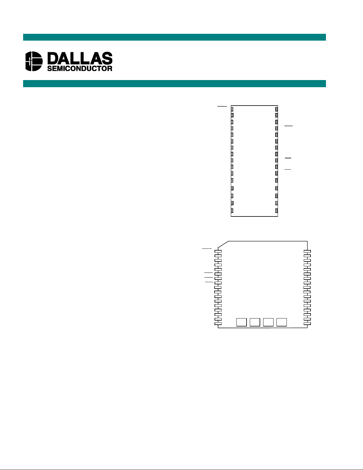
PIN ASSIGNMENT
A18/RST
RST
A15
A16
NC
V
CC
WE
OE
CE
DQ7
DQ6
DQ5
DQ4
DQ3
DQ2
DQ1
DQ0
GND
A16
A14
A12
DQ0
DQ1
DQ2
GND
32-Pin Encapsulated Package
A7
A6
A5
A4
A3
A2
A1
A0
1
2
3
4
5
6
7
8
9
10
11
12
13
14
15
16
17
1
2
3
4
5
6
7
8
9
10
11
12
13
14
15
16
740mil Flush
X1 GND
V
32
31
30
29
28
27
26
25
24
23
22
21
20
19
18
17
V
BAT
X2
CC
15
17
WE
8
11
OE
10
CE
DQ7
DQ6
DQ5
DQ4
DQ3
34
33
32
31
30
29
28
27
26
25
24
23
22
21
20
19
18
18
17
14
13
12
11
10
8
6
5
3
1
0
34-Pin PowerCap Module Board
(Uses DS9034PCX PowerCap)
PowerCap is a registered trademark of Dallas Semiconductor.
1 of 22 112801
Page 2

DS1251/DS1251P
ORDERING INFORMATION
DS1251YP–XXXY (5V)
- IND Industrial
- 70 70ns access
blank 32-Pin DIP Module
P 34-Pin PowerCap Module board*
DS1251WP-XXXY (3.3V)
- IND Industrial
- 120 120ns access
blank 32-Pin DIP Module
P 34-Pin PowerCap Module board*
*DS9034PCX (PowerCap) Required:
(Must be ordered separately.)
PIN DESCRIPTION
A0–A18 - Address Inputs
CE - Chip Enable
OE - Output Enable
WE - Write Enable
V
CC
GND - Ground
–DQ7 - Data In/Data Out
DQ
0
NC - No Connection
X1, X2 - Crystal Connection
V
BAT
RST - Reset
- Power Supply Input
- Battery Connection
DESCRIPTION
The DS1251 4096k NV SRAM with Phantom Clock is a fully static nonvolatile RAM (organized as 512k
words by 8 bits) with a built-in real-time clock. The DS1251Y has a self-contained lithium energy source
and control circuitry, which constantly monitors V
for an out-of-tolerance condition. When such a
CC
condition occurs, the lithium energy source is automatically switched on and write protection is
unconditionally enabled to prevent garbled data in both the memory and real-time clock.
The phantom clock provides timekeeping information including hundredths of seconds, seconds, minutes,
hours, days, dates, months, and years. The date at the end of the month is automatically adjusted for
months with fewer than 31 days, including correction for leap years. The phantom clock operates in either
24-hour or 12-hour format with an AM/PM indicator.
PACKAGES
The DS1251 is available in two packages: 32-pin DIP and 34-pin PowerCap module. The 32-pin DIP
style module integrates the crystal, lithium energy source, and silicon in one package. The 34-pin
PowerCap module board is designed with contacts for connection to a separate PowerCap (DS9034PCX)
that contains the crystal and battery. This design allows the PowerCap to be mounted on top of the
DS1251P after the completion of the surface mount process. Mounting the PowerCap after the surface
mount process prevents damage to the crystal and battery because of the high temperatures required for
solder reflow. The PowerCap is keyed to prevent reverse insertion. The PowerCap Module Board and
PowerCap are ordered separately and shipped in separate containers.
2 of 22
Page 3

DS1251/DS1251P
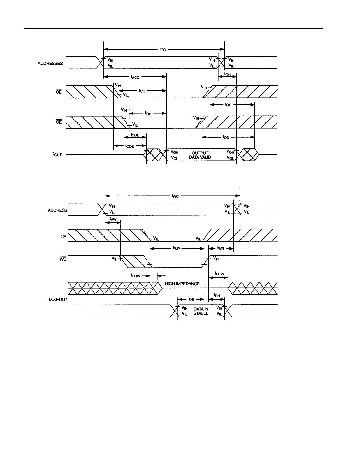
RAM READ MODE
The DS1251 executes a read cycle whenever WE (write enable) is inactive (high) and CE (chip enable) is
active (low). The unique address specified by the 19 address inputs (A0–A18) defines which of the 512k
bytes of data is to be accessed. Valid data will be available to the eight data-output drivers within t
(access time) after the last address input signal is stable, providing that CE and OE (output enable) access
times and states are also satisfied. If OE and CE access times are not satisfied, then data access must be
ACC
measured from the later occurring signal ( CE or OE ) and the limiting parameter is either t
t
for OE , rather than address access.
OE
for CE or
CO
RAM WRITE MODE
The DS1251 is in the write mode whenever the WE and CE signals are in the active (low) state after
address inputs are stable. The latter occurring falling edge of CE or WE will determine the start of the
write cycle. The write cycle is terminated by the earlier rising edge of CE or WE . All address inputs must
be kept valid throughout the write cycle. WE must return to the high state for a minimum recovery time
(t
) before another cycle can be initiated. The OE control signal should be kept inactive (high) during
WR
write cycles to avoid bus contention. However, if the output bus has been enabled ( CE and OE active)
then WE will disable the outputs in t
from its falling edge.
ODW
DATA RETENTION MODE
The 5V device is fully accessible and data can be written or read only when VCC is greater than VPF.
However, when VCC is below the power-fail point, VPF (point at which write protection occurs), the
internal clock registers and SRAM are blocked from any access. When VCC falls below the battery switch
point, V
operation and SRAM data are maintained from the battery until VCC is returned to nominal levels.
(battery supply level), device power is switched from the VCC pin to the backup battery. RTC
SO
The 3.3V device is fully accessible and data can be written or read only when V
When V
the device power is switched from VCC to the backup supply (V
greater than V
below V
falls below the power-fail point, VPF , access to the device is inhibited. If VPF is less than VBAT,
CC
) when VCC drops below V
BAT
, the device power is switched from V
BAT
. RTC operation and SRAM data are maintained from the battery until VCC is returned to
BAT
to the backup supply (VBAT ) when VCC drops
CC
is greater than V
CC
. If VPF is
PF
PF.
nominal levels.
All control, data, and address signals must be powered down when VCC is powered down.
PHANTOM CLOCK OPERATION
Communication with the phantom clock is established by pattern recognition on a serial bit stream of
64 bits, which must be matched by executing 64 consecutive write cycles containing the proper data on
DQ0. All accesses that occur prior to recognition of the 64-bit pattern are directed to memory.
After recognition is established, the next 64 read or write cycles either extract or update data in the
phantom clock, and memory access is inhibited.
Data transfer to and from the timekeeping function is accomplished with a serial bit stream under control
of chip enable, output enable, and write enable. Initially, a read cycle to any memory location using the
3 of 22
Page 4

DS1251/DS1251P
CE and OE control of the phantom clock starts the pattern recognition sequence by moving a pointer to
the first bit of the 64-bit comparison register. Next, 64 consecutive write cycles are executed using the
CE and WE control of the SmartWatch. These 64 write cycles are used only to gain access to the
phantom clock. Therefore, any address to the memory in the socket is acceptable. However, the write
cycles generated to gain access to the phantom clock are also writing data to a location in the mated
RAM. The preferred way to manage this requirement is to set aside just one address location in RAM as a
phantom clock scratch pad. When the first write cycle is executed, it is compared to bit 0 of the 64-bit
comparison register. If a match is found, the pointer increments to the next location of the comparison
register and awaits the next write cycle. If a match is not found, the pointer does not advance and all
subsequent write cycles are ignored. If a read cycle occurs at any time during pattern recognition, the
present sequence is aborted and the comparison register pointer is reset. Pattern recognition continues for
a total of 64 write cycles as described above until all the bits in the comparison register have been
matched (Figure 1). With a correct match for 64 bits, the phantom clock is enabled and data transfer to or
from the timekeeping registers can proceed. The next 64 cycles will cause the phantom clock to either
receive or transmit data on DQ0, depending on the level of the OE pin or the WE pin. Cycles to other
locations outside the memory block can be interleaved with CE cycles without interrupting the pattern
recognition sequence or data transfer sequence to the phantom clock.
PHANTOM CLOCK REGISTER INFORMATION
The phantom clock information is contained in eight registers of 8 bits, each of which is sequentially
accessed 1 bit at a time after the 64-bit pattern recognition sequence has been completed. When updating
the phantom clock registers, each register must be handled in groups of 8 bits. Writing and reading
individual bits within a register could produce erroneous results. These read/write registers are defined in
Figure 2.
Data contained in the phantom clock register is in binary-coded decimal format (BCD). Reading and
writing the registers is always accomplished by stepping through all eight registers, starting with bit 0 of
register 0 and ending with bit 7 of register 7.
4 of 22
Page 5
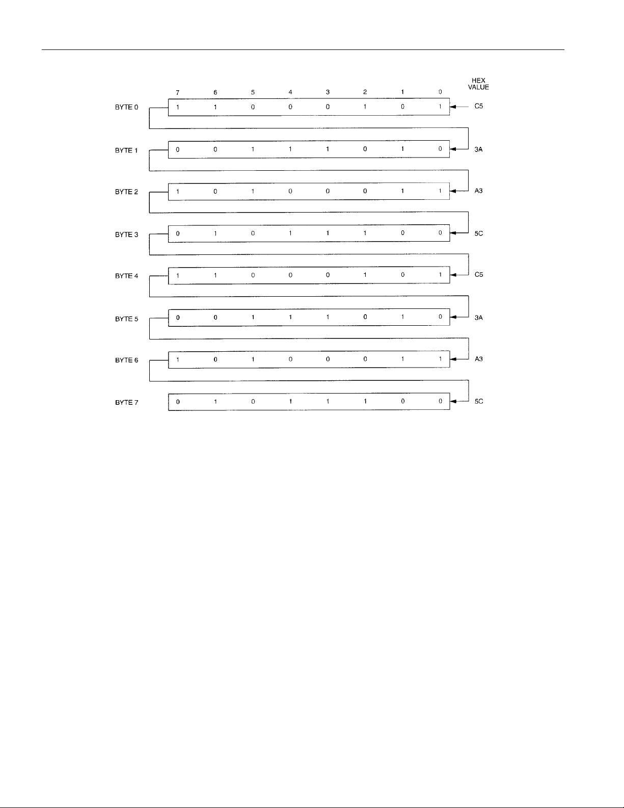
PHANTOM CLOCK REGISTER DEFINITION Figure 1
DS1251/DS1251P
Note: The pattern recognition in Hex is C5, 3A, A3, 5C, C5, 3A, A3, 5C. The odds of this pattern being
accidentally duplicated and causing inadvertent entry to the phantom clock is less than 1 in 1019. This
pattern is sent to the phantom clock LSB to MSB.
5 of 22
Page 6
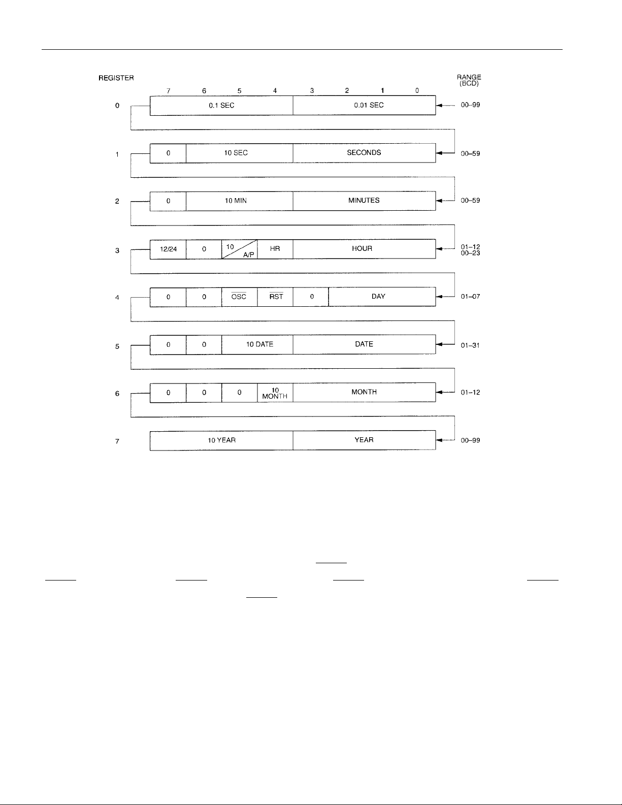
PHANTOM CLOCK REGISTER DEFINITION Figure 2
DS1251/DS1251P
AM/PM/12/24 MODE
Bit 7 of the hours register is defined as the 12-hour or 24-hour mode-select bit. When high, the 12-hour
mode is selected. In the 12-hour mode, bit 5 is the AM/PM bit with logic high being PM. In the 24-hour
mode, bit 5 is the second 10-hour bit (20–23 hours).
OSCILLATOR AND RESET BITS
Bits 4 and 5 of the day register are used to control the RESET and oscillator functions. Bit 4 controls the
RESET (pin 1). When the RESET bit is set to logic 1, the RESET input pin is ignored. When the RESET
bit is set to logic 0, a low input on the RESET pin will cause the phantom clock to abort data transfer
without changing data in the watch registers. Bit 5 controls the oscillator. When set to logic 1, the
oscillator is off. When set to logic 0, the oscillator turns on and the watch becomes operational. These bits
are shipped from the factory set to a logic 1.
ZERO BITS
Registers 1, 2, 3, 4, 5, and 6 contain one or more bits which will always read logic 0. When writing these
locations, either a logic 1 or 0 is acceptable.
6 of 22
Page 7

DS1251/DS1251P
BATTERY LONGEVITY
The DS1251 has a lithium power source that is designed to provide energy for clock activity, and clock
and RAM data retention when the V
supply is not present. The capability of this internal power supply
CC
is sufficient to power the DS1251 continuously for the life of the equipment in which it is installed. For
specification purposes, the life expectancy is 10 years at +25°C with the internal clock oscillator running
in the absence of V
power. Each DS1251 is shipped from Dallas Semiconductor with its lithium energy
CC
source disconnected, guaranteeing full energy capacity. When VCC is first applied at a level greater than
VPF, the lithium energy source is enabled for battery-backup operation. Actual life expectancy of the
DS1251 will be much longer than 10 years since no lithium battery energy is consumed when VCC is
present.
CLOCK ACCURACY (DIP MODULE)
The DS1251 is guaranteed to keep time accuracy to within ±1 minute per month at +25°C. The clock is
calibrated at the factory by Dallas Semiconductor using special calibration nonvolatile tuning elements.
The DS1251 does not require additional calibration and temperature deviations will have a negligible
effect in most applications. For this reason, methods of field clock calibration are not available and not
necessary.
CLOCK ACCURACY (POWERCAP MODULE)
The DS1251P and DS9034PCX are each individually tested for accuracy. Once mounted together, the
module is guaranteed to keep time accuracy to within ±1.53 minutes per month (35ppm) at +25°C.
7 of 22
Page 8

DS1251/DS1251P
ABSOLUTE MAXIMUM RATINGS*
Voltage Range on Any Pin Relative to Ground -0.3V to +6.0V
Soldering Temperature Range +260°C for 10 seconds (DIP) (Note 13)
See IPC/JEDEC Standard J-STD-020A for
Surface Mount Devices
* This is a stress rating only and functional operation of the device at these or any other conditions
beyond those indicated in the operation sections of this specification is not implied. Exposure to
absolute maximum rating conditions for extended periods of time can affect reliability.
OPERATING RANGE
RANGE TEMP. RANGE (ºC) VCC (V)
Commercial 0 to +70
Industrial -40 to +85
3.3 ± 10% or 5 ± 10%
3.3 ± 10% or 5 ± 10%
RECOMMENDED DC OPERATING CONDITIONS Over the operating range
PARAMETER SYMBOL MIN TYP MAX UNITS NOTES
Logic 1 Voltage All Inputs
V
VCC
= 5V ± 10%
CC
= 3.3V ± 10%
Logic 0 Voltage All Inputs
V
VCC
= 5V ± 10%
CC
= 3.3V ± 10%
V
V
IH
IL
2.2 VCC+ 0.3V V 11
2.0 VCC + 0.3V V 11
-0.3 0.8 V 11
-0.3 0.6 V 11
8 of 22
Page 9

DS1251/DS1251P
DC ELECTRICAL CHARACTERISTICS Over the operating range (5V)
PARAMETER SYMBOL MIN TYP MAX UNITS NOTES
Input Leakage Current
I/O Leakage Current
CE ³ VIH ≤ V
CC
Output Current @ 2.4V I
Output Current @ 0.4V I
Standby Current CE = 2.2V
I
I
IL
I
IO
OH
OL
CCS1
-1.0 +1.0
-1.0 +1.0
mA
mA
-1.0 mA
2.0 mA
510mA
12
Standby Current
I
CCS2
3.0 5.0 mA
CE = VCC - 0.5V
Operating Current t
Write Protection Voltage V
Battery Switchover Voltage V
= 70ns I
CYC
CC01
PF
SO
85 mA
4.25 4.37 4.50 V 11
V
BAT
V11
DC ELECTRICAL CHARACTERISTICS Over the operating range (3.3V)
PARAMETER SYMBOL MIN TYP MAX UNITS NOTES
Input Leakage Current I
I/O Leakage Current
CE ³ VIH ≤ V
CC
Output Current @ 2.4V I
Output Current @ 0.4V I
Standby Current CE = 2.2V
Standby Current
I
I
CE = VCC - 0.5V
Operating Current t
= 70ns I
CYC
Write Protection Voltage V
Battery Switchover Voltage V
IL
I
IO
OH
OL
CCS1
CCS2
CC01
PF
SO
-1.0 +1.0
-1.0 +1.0
mA
mA
12
-1.0 mA
2.0 mA
57mA
2.0 3.0 mA
50 mA
2.80 2.97 V 11
V
BAT
or V
PF
V11
CAPACITANCE (T
PARAMETER SYMBOL MIN TYP MAX UNITS NOTES
Input Capacitance C
Input/Output Capacitance C
IN
I/O
9 of 22
510pF
510pF
= +25°C)
A
Page 10

DS1251/DS1251P
MEMORY AC ELECTRICAL CHARACTERISTICS Over the operating range (5V)
PARAMETER SYMBOL
Read Cycle Time t
Access Time t
OE to Output Valid
CE to Output Valid
OE or CE to Output Active
Output High-Z from Deselection t
Output Hold from Address Change t
Write Cycle Time t
Write Pulse Width t
Address Setup Time t
Write Recovery Time t
Output High-Z from WE
Output Active from WE
Data Setup Time t
Data Hold Time from WE
RC
ACC
t
OE
t
CO
t
COE
OD
OH
WC
WP
AW
WR
t
ODW
t
OEW
DS
t
DH
DS1251Y-70
MIN MAX
UNITS NOTES
70 ns
70 ns
35 ns
70 ns
5ns5
25 ns 5
5ns
70 ns
50 ns 3
0ns
0ns
25 ns 5
5ns5
30 ns 4
5ns4
10 of 22
Page 11

PHANTOM CLOCK AC ELECTRICAL CHARACTERISTICS
Over the operating range (5V)
PARAMETER SYMBOL MIN TYP MAX UNITS NOTES
Read Cycle Time t
CE Access Time
OE Access Time
CE to Output Low-Z
OE to Output Low-Z
CE to Output High-Z
OE to Output High-Z
Read Recovery t
Write Cycle Time t
Write Pulse Width t
Write Recovery t
Data Setup Time t
Data Hold Time t
CE Pulse Width
RESET Pulse Width
RC
t
CO
t
OE
t
COE
t
OEE
t
OD
t
ODO
RR
WC
WP
WR
DS
DH
t
CW
t
RST
65 ns
5ns
5ns
10 ns
65 ns
55 ns 3
10 ns 10
30 ns 4
0ns4
60 ns
65 ns
DS1251/DS1251P
55 ns
55 ns
25 ns 5
25 ns 5
POWER-DOWN/POWER-UP TIMING Over the operating range (3.3V)
PARAMETER SYMBOL MIN TYP MAX UNITS NOTES
CE at V
before Power-Down
IH
VCC Slew from V
V
PF(min)
( CE at VPF)
VCC Slew from V
VCC Slew from V
V
CE at V
PF(min)
( CE at VPF)
after Power-Up
IH
PF(max)
PF(min)
PF(max)
to
to V
to
SO
t
t
t
PD
t
F
FB
t
R
REC
0
300
10
0
ms
ms
ms
ms
1.5 2.5 ms
(TA = +25°C)
PARAMETER SYMBOL MIN TYP MAX UNITS NOTES
Expected Data Retention Time t
DR
Warning: Under no circumstances are negative undershoots of any amplitude allowed when device is in
battery-backup mode.
10 years 9
11 of 22
Page 12

MEMORY AC ELECTRICAL CHARACTERISTICS
PARAMETER SYMBOL
Read Cycle Time t
Access Time t
OE to Output Valid
CE to Output Valid
OE or CE to Output Active
Output High-Z from Deselection t
Output Hold from Address Change t
Write Cycle Time t
Write Pulse Width t
Address Setup Time t
Write Recovery Time t
Output High-Z from WE
Output Active from WE
Data Setup Time t
Data Hold Time from WE
RC
ACC
t
OE
t
CO
t
COE
OD
OH
WC
WP
AW
WR
t
ODW
t
OEW
DS
t
DH
DS1251W-120
MIN MAX
120 ns
5ns5
5ns
120 ns
90 ns 3
0ns
20 ns 10
5ns5
50 ns 4
20 ns 4
DS1251/DS1251P
Over the operating range (3.3V)
UNITS NOTES
120 ns
60 ns
120 ns
40 ns 5
40 ns 5
PHANTOM CLOCK AC ELECTRICAL CHARACTERISTICS
Over the operating range (3.3V)
PARAMETER SYMBOL MIN TYP MAX UNITS NOTES
Read Cycle Time t
CE Access Time
OE Access Time
CE to Output Low-Z
OE to Output Low-Z
CE to Output High-Z
OE to Output High-Z
Read Recovery t
Write Cycle Time t
Write Pulse Width t
Write Recovery t
Data Setup Time t
Data Hold Time t
CE Pulse Width
RESET Pulse Width
t
t
t
COE
t
OEE
t
t
ODO
t
t
RST
RC
CO
OE
OD
RR
WC
WP
WR
DS
DH
CW
120 ns
100 ns
100 ns
5ns
5ns
40 ns 5
40 ns 5
20 ns
120 ns
100 ns 3
20 ns 10
45 ns 4
0ns4
105 ns
120 ns
12 of 22
Page 13

DS1251/DS1251P
POWER-DOWN/POWER-UP TIMING Over the operating range (3.3V)
PARAMETER SYMBOL MIN TYP MAX UNITS NOTES
CE at V
before Power-Down
IH
VCC Slew from V
V
PF(min)
( CE at VIH)
VCC Slew from V
V
CE at V
PF(min)
( CE at VIH)
after Power-Up
IH
PF(max)
PF(max)
to
to
t
t
PD
t
F
t
R
REC
0
300
0
ms
ms
ms
1.5 2.5 ms
(TA = +25°C)
PARAMETER SYMBOL MIN TYP MAX UNITS NOTES
Expected Data Retention Time t
DR
Warning: Under no circumstances are negative undershoots of any amplitude allowed when device is in
battery-backup mode.
10 years 9
13 of 22
Page 14
MEMORY READ CYCLE (Note 1)
MEMORY WRITE CYCLE 1 (Notes 2, 6, and 7)
DS1251/DS1251P
14 of 22
Page 15

MEMORY WRITE CYCLE 2 (Notes 2 and 8)
DS1251/DS1251P
RESET FOR PHANTOM CLOCK
READ CYCLE TO PHANTOM CLOCK
15 of 22
Page 16

WRITE CYCLE TO PHANTOM CLOCK
)
POWER-DOWN/POWER-UP CONDITION (5V
DS1251/DS1251P
16 of 22
Page 17

POWER-DOWN/POWER-UP CONDITION (3.3V
)
DS1251/DS1251P
17 of 22
Page 18

AC TEST CONDITIONS
Output Load: 50pF + 1TTL Gate
Input Pulse Levels: 0V to 3V
NOTES:
1) WE is high for a read cycle.
DS1251/DS1251P
Timing Measurement Reference Levels
Input: 1.5V
Output: 1.5V
Input Pulse Rise and Fall Times: 5ns
OE = V
2)
or VIL. If OE = VIH during write cycle, the output buffers remain in a high impedance
IH
state.
t
3)
4)
5)
6)
is specified as the logical AND of CE and WE . tWP is measured from the latter of CE or WE
WP
going low to the earlier of
t
, t DS are measured from the earlier of CE or WE going high.
DH
CE or WE going high.
These parameters are sampled with a 50pF load and are not 100% tested.
If the CE low transition occurs simultaneously with or later than the WE low transition in Write
Cycle 1, the output buffers remain in a high impedance state during this period.
7)
If the CE high transition occurs prior to or simultaneously with the WE high transition, the output
buffers remain in a high impedance state during this period.
If WE is low or the WE low transition occurs prior to or simultaneously with the CE low transition,
8)
the output buffers remain in a high impedance state during this period.
9)
The expected t
is defined as cumulative time in the absence of VCC with the clock oscillator
DR
running.
t
10)
11)
12)
13)
is a function of the latter occurring edge of WE or CE .
WR
Voltages are referenced to ground.
RST (Pin 1) has an internal pullup resistor.
Real-time clock modules can be successfully processed through conventional wave-soldering
techniques as long as temperature exposure to the lithium energy source contained within does not
exceed +85°C. Post-solder cleaning with water-washing techniques is acceptable, provided that
ultrasonic vibration is not used.
In addition, for the PowerCap:
1)
Dallas Semiconductor recommends that PowerCap Module bases experience one pass through solder
reflow oriented with the label side up (“live-bug”).
2)
Hand soldering and touch-up: Do not touch or apply the soldering iron to leads for more than three
seconds.
- To solder, apply flux to the pad, heat the lead frame pad, and apply solder. To remove the part,
apply flux, heat the lead frame pad until the solder reflows, and use a solder wick to remove
solder.
18 of 22
Page 19

DS1251 4096k NV SRAM WITH PHANTOM CLOCK
DS1251/DS1251P
KG 32-PIN
DIM MIN MAX
A IN.
MM
B IN.
MM
C IN.
MM
D IN.
MM
E IN.
MM
F IN.
MM
G IN.
MM
H IN.
MM
J IN.
MM
K IN.
MM
1.680
42.67
0.715
18.16
0.335
8.51
0.075
1.91
0.015
0.38
0.140
3.56
0.090
2.29
0.590
14.99
0.010
0.25
0.015
0.38
1.740
44.20
0.740
18.80
0.365
9.27
0.105
2.67
0.030
0.76
0.180
4.57
0.110
2.79
0.630
16.00
0.018
0.46
0.025
0.64
19 of 22
Page 20

DS1251P
DS1251/DS1251P
PKG INCHES
DIM MIN NOM MAX
A
0.920 0.925 0.930
B
0.980 0.985 0.990
C
D
E
F
G
- - 0.080
0.052 0.055 0.058
0.048 0.050 0.052
0.015 0.020 0.025
0.025 0.027 0.030
Note: Dallas Semiconductor recommends that PowerCap Module bases experience one pass through
solder reflow oriented with the label side up (“live-bug”).
Hand soldering and touch-up: Do not touch or apply the soldering iron to leads for more than three
seconds.
To solder, apply flux to the pad, heat the lead frame pad, and apply solder. To remove the part, apply flux,
heat the lead frame pad until the solder reflows, and use a solder wick to remove solder.
20 of 22
Page 21

DS1251P WITH DS9034PCX ATTACHED
DS1251/DS1251P
PKG INCHES
DIM MIN NOM MAX
A
B
C
D
E
F
G
0.920 0.925 0.930
0.955 0.960 0.965
0.240 0.245 0.250
0.052 0.055 0.058
0.048 0.050 0.052
0.015 0.020 0.025
0.020 0.025 0.030
COMPONENTS AND PLACEMENT MAY
VARY FROM EACH DEVICE TYPE
21 of 22
Page 22

RECOMMENDED POWERCAP MODULE LAND PATTERN
DS1251/DS1251P
PKG INCHES
DIM MIN NOM MAX
A
B
C
D
E
- 1.050 -
- 0.826 -
- 0.050 -
- 0.030 -
- 0.112 -
22 of 22
 Loading...