

Page 1
DS1202, DS1202S
DS1202, DS1202S
Serial Timekeeping Chip
FEATURES
• Real time clock counts seconds, minutes, hours, date
of the month, month, day of the week, and year with
leap year compensation valid up to 2100
• 24 x 8 RAM for scratchpad data storage
• Serial I/O for minimum pin count
• 2.0–5.5 volt full operation
• Uses less than 300 nA at 2 volts
• Single–byte or multiple–byte (burst mode) data trans-
fer for read or write of clock or RAM data
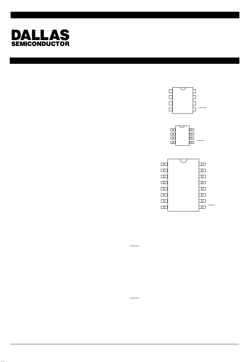
• 8–pin DIP or optional 16–pin SOIC for surface mount
• Simple 3–wire interface
• TTL–compatible (V
CC
= 5V)
• Optional industrial temperature range –40°C to +85°C
(IND)
ORDERING INFORMATION
DS1202 8–pin DIP
DS1202S 16–pin SOIC
DS1202S–8 8–pin SOIC
DS1202N 8–pin DIP (IND)
DS1202SN 16–pin SOIC (IND)
DS1202SN–8 8–pin SOIC (IND)
DESCRIPTION
The DS1202 Serial Timekeeping Chip contains a real
time clock/calendar and 24 bytes of static RAM. It communicates with a microprocessor via a simple serial interface. The real time clock/calendar provides seconds,
minutes, hours, day, date, month, and year information.
The end of the month date is automatically adjusted for
months with less than 31 days, including corrections for
leap year. The clock operates in either the 24–hour or
12–hour format with an AM/PM indicator. Interfacing the
PIN ASSIGNMENT
V
8
CC
7
SCLK
6
I/O
5
RST
8
V
CC
7
SCLK
6
I/O
5
RST
16
V
15
14
13
12
11
10
CC
NC
SCLK
NC
I/O
NC
NC
9
RST
NC
NC
NC
NC
NC
GND
NC
1
X1
2
X2
3
GND
4
8–PIN DIP
1
NC
2
X1
3
X2
4
GND
8–PIN SOIC
(208 mil)
1
2
3
X1
4
5
X2
6
7
8
16–PIN SOIC
PIN DESCRIPTION
NC – No Connection
X1, X2 – 32.768 KHz Crystal Input
GND – Ground
RST
I/O – Data Input/Output
SCLK – Serial Clock
V
CC
DS1202 with a microprocessor is simplified by using
synchronous serial communication. Only three wires
are required to communicate with the clock/RAM: (1)
(Reset), (2) I/O (Data line), and (3) SCLK (Serial
RST
clock). Data can be transferred to and from the clock/
RAM one byte at a time or in a burst of up to 24 bytes.
The DS1202 is designed to operate on very low power
and retain data and clock information on less than 1 microwatt.
– Reset
– Power Supply Pin
Copyright 1997 by Dallas Semiconductor Corporation.
All Rights Reserved. For important information regarding
patents and other intellectual property rights, please refer to
Dallas Semiconductor data books.
032697 1/11
Page 2
DS1202, DS1202S
OPERATION
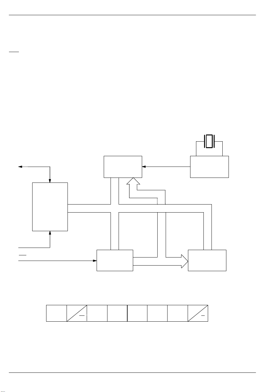
The main elements of the Serial Timekeeper are shown
in Figure 1: shift register, control logic, oscillator, real
time clock, and RAM. To initiate any transfer of data,
is taken high and eight bits are loaded into the shift
RST
register providing both address and command information. Data is serially input on the rising edge of the SCLK.
The first eight bits specify which of 32 bytes will be accessed, whether a read or write cycle will take place,
and whether a byte or burst mode transfer is to occur.
After the first eight clock cycles have occurred which
load the command word into the shift register, additional
clocks will output data for a read or input data for a write.
DS1202 BLOCK DIAGRAM Figure 1
I/O
INPUT SHIFT
REGISTERS
REAL TIME
CLOCK
The number of clock pulses equals eight plus eight for
byte mode or eight plus up to 192 for burst mode.
COMMAND BYTE
The command byte is shown in Figure 2. Each data
transfer is initiated by a command byte. The MSB (Bit 7)
must be a logic 1. If it is zero, further action will be terminated. Bit 6 specifies clock/calendar data if logic 0 or
RAM data if logic 1. Bits one through five specify the
designated registers to be input or output, and the LSB
(Bit 0) specifies a write operation (input) if logic 0 or read
operation (output) if logic 1. The command byte is always input starting with the LSB (bit 0).
32.768 KHz
X2X1
OSCILLATOR
AND DIVIDER
DATA BUS
SCLK
RST
COMMAND AND
CONTROL LOGIC
ADDRESS/COMMAND BYTE Figure 2
RAM
6
CK
5
A4
7
1
032697 2/11
ADDRESS BUS
4
A3
3
A2
2
A1
1
A0
24 X 8 RAM
0
RD
W
Page 3

DS1202, DS1202S
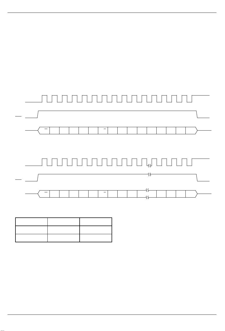
RESET AND CLOCK CONTROL
All data transfers are initiated by driving the RST input
high. The RST input serves two functions. First, RST
turns on the control logic which allows access to the shift
register for the address/command sequence. Second,
signal provides a method of terminating either
the RST
single byte or multiple byte data transfer. A clock cycle is
a sequence of a falling edge followed by a rising edge.
For data inputs, data must be valid during the rising
edge of the clock and data bits are output on t he falling
edge of clock. All data transfer terminates if the RST
put is low and the I/O pin goes to a high impedance
state. Data transfer is illustrated in Figure 3.
in-
DATA INPUT
Following the eight SCLK cycles that input a write command byte, a data byte is input on the rising edge of the
next eight SCLK cycles. Additional SCLK cycles are ignored should they inadvertently occur. Data is input
starting with bit 0. Due to the inherent nature of the logic
state machine, writing times containing an absolute
value of “59” seconds should be avoided.
DATA OUTPUT
Following the eight SCLK cycles that input a read command byte, a data byte is output on the falling edge of
the next eight SCLK cycles. Note that the first data bit to
be transmitted occurs on the first falling edge after the
last bit of the command byte is written. Additional SCLK
cycles retransmit the data bytes should they inadvertently occur so long as RST
tion permits continuous burst mode read capability.
Data is output starting with bit 0.
remains high. This opera-
Each byte that is written to will be transferred to RAM
regardless of whether all 24 bytes are written or not.
CLOCK/CALENDAR
The clock/calendar is contained in eight write/read registers as shown in Figure 4. Data contained in the clock/
calendar registers is in binary coded decimal format
(BCD).
CLOCK HALT FLAG
Bit 7 of the seconds register is defined as the clock halt
flag. When this bit is set to logic 1, the clock oscillator is
stopped and the DS1202 is placed into a low–power
standby mode with a current drain of not more than 100
nanoamps. When this bit is written to logic 0, the clock
will start.
AM–PM/12–24 MODE
Bit 7 of the hours register is defined as the 12– or
24–hour mode select bit. When high, the 12–hour mode
is selected. In the 12–hour mode, bit 5 is the AM/PM bit
with logic high being PM. In the 24–hour mode, bit 5 is
the second 10 hour bit (20–23 hours).
WRITE PROTECT BIT
Bit 7 of the control register is the write protect bit. The
first seven bits (bits 0–6) are forced to zero and will always read a zero when read. Before any write operation
to the clock or RAM, bit 7 must be zero. When high, the
write protect bit prevents a write operation to any other
register.
BURST MODE
Burst mode may be specified for either the clock/calendar or the RAM registers by addressing location 31 decimal (address/command bits one through five = logical
one). As before, bit six specified clock or RAM and bit 0
specifies read or write. There is no data storage capacity at locations 8 through 31 in the Clock/Calendar Registers or locations 24 through 31 in the RAM registers.
When writing to the clock registers in the burst mode,
the first eight registers must be written in order for the
data to be transferred.
However, when writing to RAM in burst mode it is not
necessary to write all 24 bytes for the data to transfer.
CLOCK/CALENDAR BURST MODE
The clock/calendar command byte specifies burst
mode operation. In this mode the eight clock/calendar
registers can be consecutively read or written (see Figure 4) starting with bit 0 of address 0.
RAM
The static RAM is 24 x 8 bytes addressed consecutively
in the RAM address space.
RAM BURST MODE
The RAM command byte specifies burst mode operation. In this mode, the 24 RAM registers can be consecutively read or written (see Figure 4) starting with bit 0 of
address 0.
032697 3/11
Page 4
DS1202, DS1202S
REGISTER SUMMARY
A register data format summary is shown in Figure 4.
CRYSTAL SELECTION
A 32.768 KHz crystal, can be directly connected to the
DS1202 via pins 2 and 3 (X1, X2). The crystal selected
for use should have a specified load capacitance (CL) of
6 pF . The crystal is connected directly to the X1 and X2
DATA TRANSFER SUMMARY Figure 3
SINGLE BYTE TRANSFER
SCLK
RST
I/O
BURST MODE TRANSFER
SCLK
0123456701 23456 7
R/W
A0 A1 A2 A3 A4 1
ADDRESS COMMAND DATA INPUT/OUTPUT
R/C
pins. There is no need for external capacitors or resistors. Note: X1 and X2 are very high impedance nodes.
It is recommended that they and the crystal be guard–
ringed with ground and that high frequency signals be
kept away from the crystal area. For more information
on crystal selection and crystal layout considerations,
please consult Application Note 58, “Crystal Considerations with Dallas Real Time Clocks”.
RST
I/O
0123456701 2 456 7
R/W
11111 1
ADDRESS COMMAND DATA I/O BYTE N
FUNCTION BYTE N SCLK n
CLOCK 8 72
RAM 24 200
032697 4/11
R/C
DATA I/O BYTE 1
Page 5

REGISTER ADDRESS/DEFINITION Figure 4
REGISTER ADDRESS REGISTER DEFINITION
A. CLOCK
0
1
RD
W
00–59
CH SEC10 SEC
SEC
7
6
1
050403020
0
DS1202, DS1202S
MIN
HR
DATE
MONTH
DAY
YEAR
CONTROL
CLOCK
BURST
B. RAM
1 0 0 0 0 1
0
1 0 0 0 1 0
0
1 0 0 0 1 1
0
1 0 0 1 0 0
0
1 0 0 1 0 1
0
1 0 0 1 1 0
0
1 0 0 1 1 1
0
1 1 1 1 1 1
0
RD
RD
RD
RD
RD
RD
RD
RD
0
W
W
W
W
W
W
W
W
00–59
01–12
00–23 24
01–28/29
01–30
01–31
01–12
01–07
0–99
12/
0 10 DATE0
0 0
0
0 0 00
10 YEAR
WP
10
HR HR0
A/P
10
M
FORCED TO ZERO
MIN10 MIN
DATE
MONTH
DAY0
YEAR
RAM 0
RAM 23
RAM
BURST
1 0 0 0 0 0
1
1 1 0 1 1 1
1
1 1 1 1 1 1
1
RD
RD
RD
W
W
W
RAM DATA 0
RAM DATA 23
032697 5/11
Page 6

DS1202, DS1202S
Logic 0 I
t
V
V
1
Logic 1 Output
V
V
2
Logic 0 Output
V
V
3
Acti
t
I
A
5
Timek
t
I
A
4
Leak
t
I
A
10
ABSOLUTE MAXIMUM RATINGS*
Voltage on Any Pin Relative to Ground –0.3V to +7.0V
Operating Temperature 0°C to 70°C
Storage Temperature –55°C to +125°C
Soldering Temperature 260°C for 10 seconds
* This is a stress rating only and functional operation of the device at these or any other conditions above those
indicated in the operation sections of this specification is not implied. Exposure to absolute maximum rating
conditions for extended periods of time may affect reliability.
RECOMMENDED DC OPERATING CONDITIONS (0°C to 70°C)
PARAMETER SYMBOL MIN TYP MAX UNITS NOTES
Supply Voltage V
Logic 1 Input V
npu
CC
IH
VCC=2.0V –0.3 +0.3
IL
VCC=5V –0.3 +0.8
2.0 5.5 V 1
2.0 VCC+0.3 V 1
DC ELECTRICAL CHARACTERISTICS (0°C to 70°C; VCC = 2.0 to 5.5V*)
PARAMETER SYMBOL MIN TYP MAX UNITS NOTES
Input Leakage I
I/O Leakage I
ve Supply Curren
eeping Curren
age Curren
*Unless otherwise noted.
LI
LO
OH
OL
CC
CC1
CC2
VCC=2V 1.6
VCC=5V 2.4
VCC=2V 0.4
VCC=5V 0.4
VCC=2V 0.4
VCC=5V 1.2
VCC=2V 0.3
VCC=5V 1
VCC=2V 100
VCC=5V 100
+500 µA 6
+500 µA 6
m
µ
n
CAPACITANCE (tA = 25°C)
PARAMETER SYMBOL CONDITION TYP MAX UNITS NOTES
Input Capacitance C
I/O Capacitance C
Crystal Capacitance C
032697 6/11
I
I/O
X
5 pF
10 pF
6 pF
Page 7
DS1202, DS1202S
Data to CLK Set
t
7
CLK to Data Hold
t
7
CLK to Data Del
t
7, 8, 9
CLK L
t
7
CLK High Ti
t
7, 12
CLK F
f
MHz7, 12
CLK Ri
ll
t
t
RST to CLK Set
t
7
CLK to RST Hold
t
7
RST I
t
7
RST to I/O High Z
t
7
AC ELECTRICAL CHARACTERISTICS (0°C to 70°C; VCC = 2.0 to 5.5V*)
PARAMETER SYMBOL MIN TYP MAX UNITS NOTES
up
ay
ow Time
me
requency
se and Fa
up
nactive Time
*Unless otherwise noted.
DC
CDH
CDD
CL
CH
CLK
,
R
CC
CCH
CWH
CDZ
VCC=2V 200
VCC=5V 50
VCC=2V 280
VCC=5V 70
VCC=2V 800
VCC=5V 200
VCC=2V 1000
VCC=5V 250
VCC=2V 1000
VCC=5V 250
VCC=2V 0.5
VCC=5V DC 2.0
VCC=2V 2000
F
VCC=5V 500
VCC=2V 4
VCC=5V 1
VCC=2V 1000
VCC=5V 250
VCC=2V 4
VCC=5V 1
VCC=2V 280
VCC=5V 70
ns
ns
ns
ns
ns
ns
µs
ns
µs
ns
032697 7/11
Page 8

DS1202, DS1202S
TIMING DIAGRAM: READ DATA TRANSFER Figure 5
RESET
CLOCK
DATA INPUT/
OUTPUT
t
CC
t
t
DC
017
CDH
COMMAND BYTE
TIMING DIAGRAM: WRITE DATA TRANSFER Figure 6
RESET
CLOCK
DATA INPUT/
OUTPUT
t
CC
t
CL
t
CDH
t
DC
01
t
CH
t
R
t
CDD
t
F
7
t
CCH
t
CDZ
t
CWH
COMMAND BYTE
NOTES:
1. All voltages are referenced to ground.
2. Logic one voltages are specified at a source current of 1 mA at V
capacitive loads.
3. Logic zero voltages are specified at a sink current of 4 mA at V
is specified with I/O open, RST set to a logic 0, and clock halt flag=0 (oscillator enabled).
4. I
CC1
is specified with the I/O pin open, RST high, SCLK=2 MHz at VCC=5V; SCLK=500 KHz, VCC=2V and clock
5. I
CC
halt flag=0 (oscillator enabled).
, SCLK, and I/O all have 40KΩ pull–down resistors to ground.
6. RST
7. Measured at V
8. Measured at V
=2.0V or VIL=0.8V and 10 ms maximum rise and fall time.
IH
=2.4V or VOL=0.4V.
OH
9. Load capacitance = 50 pF.
032697 8/11
=5V and 0.4 mA at VCC=2V, VOH=VCC for
CC
=5V and 1.5 mA at VCC=2V.
CC
Page 9

10.I
is specified with RST , I/O, and SCLK open. The clock halt flag must be set to logic one (oscillator disabled).
CC2
11.At power–up, RST
must be at a logic 0 until VCC2 volts. Also, SCLK must be at a logic 0 when RST is driven
to a logic one state.
12.If t
exceeds 100 ms with RST in a logic one state, then ICC may briefly exceed ICC specification.
CH
DS1202 SERIAL TIMEKEEPER 8–PIN DIP
85
8–PINPKG
DIM MIN MAX
B
1
K
4
A
C
F
E
G
A IN. 0.360 0.400
MM
B IN. 0.240 0.260
MM
C IN. 0.120 0.140
MM
D IN. 0.300 0.325
MM
E IN. 0.015 0.040
MM
F IN. 0.110 0.140
MM
G IN. 0.090 0.110
MM
H IN. 0.320 0.370
MM
J IN. 0.008 0.012
MM
K IN. 0.015 0.021
MM
DS1202, DS1202S
D
J
H
032697 9/11
Page 10

DS1202, DS1202S
DS1202S SERIAL TIMEKEEPER 16–PIN SOIC
GK
F
HB
1
A
C
E
phi
J
DIM MIN MAX
A IN. 0.500 0.511
MM 12.70 12.99
B IN. 0.290 0.300
MM 7.37 7.65
C IN. 0.089 0.095
MM 2.26 2.41
E IN. 0.004 0.012
MM 0.102 0.30
F IN. 0.094 0.105
MM 2.38 2.68
G IN.
MM
H IN. 0.398 0.416
MM 10.11 10.57
J IN. 0.009 0.013
MM 0.229 0.33
K IN. 0.013 0.019
MM 0.33 0.48
L IN 0.016 0.040
MM 0.406 1.20
phi 0° 8°
16–PINPKG
0.050 BSC
1.27 BSC
L
032697 10/11
Page 11
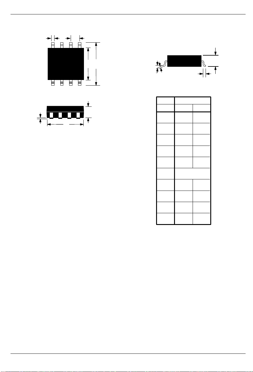
DS1202S8 8–PIN SOIC 200 MIL
K G
DS1202, DS1202S
H
B
0–8 deg. typ.
1
C
E
A
J
L
8–PINPKG
DIM MIN MAX
A IN. 0.203 0.213
MM 5.16 5.41
B IN. 0.203 0.213
MM 5.16 5.41
C IN. 0.070 0.074
MM 1.78 1.88
E IN. 0.004 0.010
MM 0.102 0.390
F IN. 0.074 0.84
MM 1.88 2.13
G IN. 0.050 BSC
MM 1.27 BSC
H IN. 0.302 0.318
MM 7.67 8.07
J IN. 0.006 0.010
MM 0.152 0.254
K IN. 0.013 0.020
MM 0.33 0.508
L IN. 0.19 0.030
MM 4.83 0.762
F
032697 11/11
 Loading...