

Page 1
General Description
The DS1099 is a low-cost, low-power, low-frequency
silicon oscillator that generates two square-wave outputs with frequencies between 0.25Hz and 1.048MHz.
Individual output enables allow both outputs to be
enabled/disabled independently. Both outputs are
capable of sinking 16mA, allowing them to directly
interface to light-emitting diodes (LEDs) as well as other
external circuitry. The DS1099 operates over a wide
supply voltage, making it suitable for both 3V and 5V
systems. The device is shipped from the factory custom
programmed and calibrated, ready to be inserted into
the end application.
Contact the factory for custom frequencies or requirements.
Applications
Flashing LED Status Indicators
Consumer Appliances
Automotive
Servers
Printers
Switch-Mode Power Supplies
Features
♦ Low-Cost, Low-Frequency EconOscillator™ with
Dual Outputs
♦ Factory Programmed
♦ Output Frequencies Independently Programmable
from 0.25Hz to 1.048MHz
♦ 2.7V to 5.5V Single-Supply Operation
♦ No External Timing Components Required
♦ Independent Output Enables
♦ CMOS/TTL-Compatible Outputs
♦ Oscillator Outputs Capable of Sinking 16mA to
Directly Drive LEDs
♦ Relieves Microprocessor of Periodic Interrupt
♦ Low-Power Consumption
♦ Operating Temperature Range: -40°C to +85°C
♦ ±100ppm/°C Temp Drift (MAX)
DS1099
Low-Frequency Dual EconOscillator
______________________________________________ Maxim Integrated Products 1
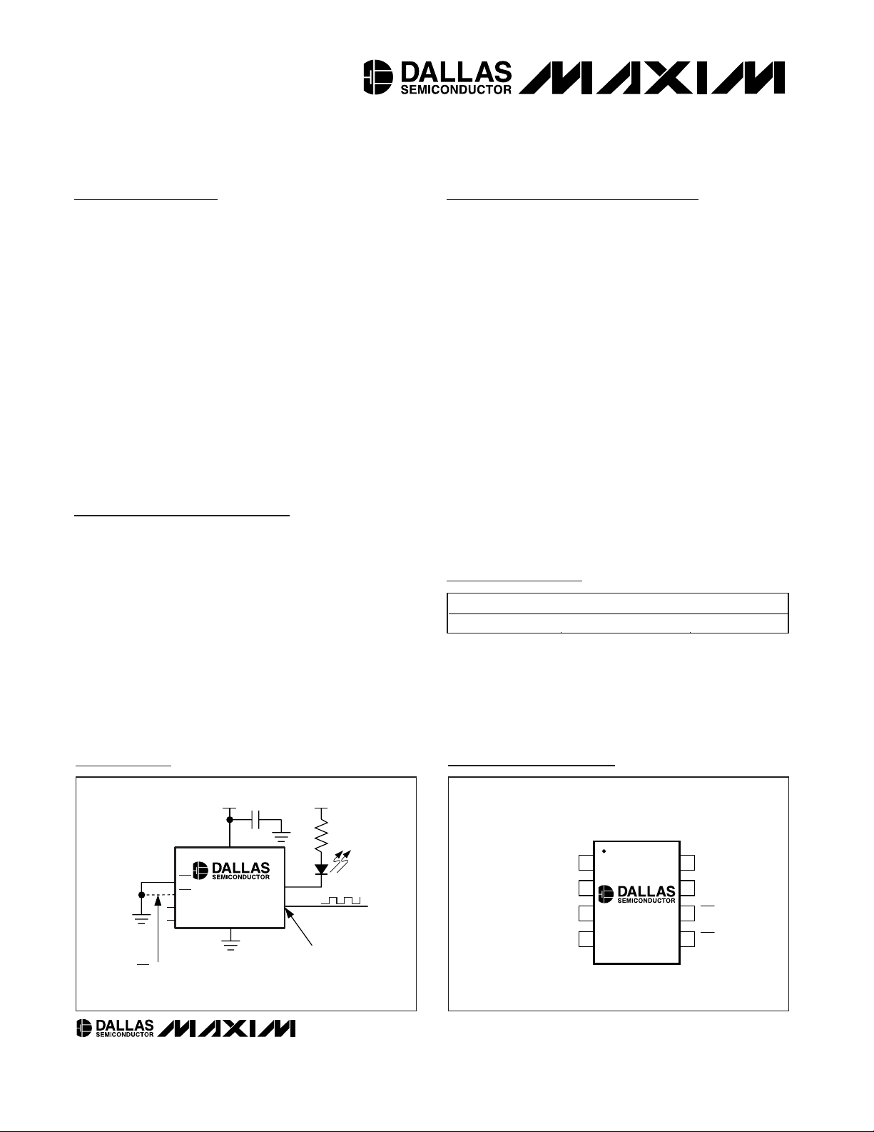
OE1
OEOGND
1
2
87N.C.
N.C.OUT0
V
CC
OUT1
µSOP
TOP VIEW
3
4
6
5
DS1099
Pin Configuration
Ordering Information
DS1099
OUT0
OUT1
GND
OE0
V
CC
V
CC
V
CC
OE1
N.C.
N.C.
OE1 CAN INSTEAD
BE TIED TO V
CC
IF OUT1 IS NOT USED.
OUTPUTS CAPABLE OF
SINKING 16mA
Typical Operating Circuit
Rev 0; 2/04
For pricing, delivery, and ordering information, please contact Maxim/Dallas Direct! at
1-888-629-4642, or visit Maxim’s website at www.maxim-ic.com.
PART TEMP RANGE
PIN-PACKAGE
DS1099U-α
0 α1
* -40°C to +85°C 8 µSOP
EconOscillator is a trademark of Dallas Semiconductor.
Ordering information is continued on the last page.
*Where α0and α1specify the factory programmed divider set-
tings for OUT0 and OUT1, respectively.
Page 2
DS1099
Low-Frequency Dual EconOscillator
2 _____________________________________________________________________
ABSOLUTE MAXIMUM RATINGS
RECOMMENDED DC OPERATING CONDITIONS
(TA= -40°C to +85°C)
Stresses beyond those listed under “Absolute Maximum Ratings” may cause permanent damage to the device. These are stress ratings only, and functional
operation of the device at these or any other conditions beyond those indicated in the operational sections of the specifications is not implied. Exposure to
absolute maximum rating conditions for extended periods may affect device reliability.
Voltage Range on VCCRelative to Ground...........-0.5V to +6.0V
Voltage Range on
OE0 and OE1
Relative to Ground.................................-0.5V to (V
CC
+ 0.5V),
not to exceed 6.0V
Operating Temperature Range ...........................-40°C to +85°C
Storage Temperature Range.............................-55°C to +125°C
Soldering Temperature.......................................See IPC/JEDEC
J-STD-020A Specification
PARAMETER
CONDITIONS
UNITS
Supply Voltage V
CC
(Note 1) 2.7 5.5 V
Input Logic 1 (OE0, OE1)V
IH
0.7 x
V
CC
+
0.3
V
Input Logic 0 (OE0, OE1)V
IL
+0.3 x
V
DC ELECTRICAL CHARACTERISTICS
(VCC= +2.7V to +5.5V, TA= -40°C to +85°C, unless otherwise noted.)
PARAMETER
CONDITIONS
UNITS
Standby Supply Current I
STBY
OE0 = OE1 = V
CC
275 µA
323
4kHz (both) 146Active Supply Current (Note 2) I
CC
CL = 15pF per output,
OE0 = OE1 = GND,
V
CC
= 3.3V
1Hz (both) 145
µA
High-Level Output Voltage
(OUT0, OUT1)
V
OH
IOH = -1mA, VCC = MIN 2.4 V
Low-Level Output Voltage
(OUT0, OUT1)
V
OL
IOL = 16mA 0.4 V
High-Level Input Current
(OE0, OE1)
I
IH
VIH = V
CC
µA
Low-Level Input Current
(OE0, OE1)
I
IL
VIL = 0.0V
µA
SYMBOL
MIN TYP MAX
V
CC
SYMBOL
1.048MHz (both)
-0.3
MIN TYP MAX
145
-1.0
V
CC
+1.0
Page 3

DS1099
Low-Frequency Dual EconOscillator
_____________________________________________________________________ 3
Note 1: All voltages referenced to ground.
Note 2: Active supply current combines the standby current with the output current. The output current is defined by
I = (C
LOAD
+ 12pF ) x VCCx f
OUT
for each output when enabled.
Note 3: This is the change observed in output frequency due to changes in temperature or voltage.
Note 4: This parameter is guaranteed by design.
Note 5: This indicates the time between power-up and the outputs becoming active.
AC ELECTRICAL CHARACTERISTICS
(VCC= +2.7V to +5.5V, TA= -40°C to +85°C, unless otherwise noted.)
PARAMETER
CONDITIONS
UNITS
Master Oscillator Frequency f
MOSC
MHz
Nominal Output Frequency
f
OUT0,
f
OUT1
Hz
Output Frequency Tolerance ∆f
OUT
TA = +25°C, VCC = 4.1V
%
TA = +25°C
ppm/V
Voltage Frequency Variation
(Note 3)
∆f
OUT
2.7V to 5.5V, TA = +25°C
%
Temperature Frequency Variation
∆f
OUT
(Notes 3, 4)
ppm/°C
Output Duty Cycle 45 55 %
Power-Up Time t
PU
(Note 5) 10 ms
Output Rise/Fall Time tR, t
F
CL = 15pF (both) 20 ns
Typical Operating Characteristics
(VCC= +5.0V, TA = +25°C, unless otherwise noted.)
SUPPLY CURRENT vs. SUPPLY VOLTAGE
V
CC
= 15pF, TA = +25°C
DS1099 toc01
SUPPLY VOLTAGE (V)
SUPPLY CURRENT (µA)
4.84.13.4
100
200
300
400
500
600
700
0
2.7 5.5
OUT0 = OUT1 = 1MHz
OUT0 = OUT1 = 0.25Hz
OUT0 =1MHz,
OUT1 = 0.25Hz
SUPPLY CURRENT vs. TEMPERATURE
V
CC
= 5.5V, CL = 15pF
DS1099 toc02
TEMPERATURE (°C)
SUPPLY CURRENT (µA)
603510-15
100
200
300
400
500
600
700
0
-40 85
OUT0 = OUT1 = 1MHz
OUT0 = OUT1 = 0.25Hz
OUT0 =1MHz,
OUT1 = 0.25Hz
SUPPLY CURRENT vs. OUTPUT LOAD
(BOTH OUTPUTS LOADED EQUALLY), T
A
= +25°C
DS1099 toc03
CL (pF)
SUPPLY CURRENT (mA)
40302010
0.2
0.4
0.6
0.8
1.0
1.2
0
050
VCC = 5.5V
VCC = 4.0V
VCC = 2.7V
SYMBOL
MIN TYP MAX
1.048
0.25 1,048,000
-1.0 +1.0
3300
-2.0 +2.5
-100 +100
Page 4

Pin Description
PIN NAME FUNCTION
1 OUT1
2 OUT0
Oscillator Outputs. Each output is forced high when the corresponding OE is high.
3VCCPositive Supply Terminal
4 GND Ground
5 OE0
6 OE1
Output Enable for OUT0 and OUT1, respectively. When low, the outputs are enabled. When high, the
corresponding output is disabled (forced high).
7, 8 N.C. No Connection
DS1099
Low-Frequency Dual EconOscillator
4 _____________________________________________________________________
Typical Operating Characteristics (continued)
(VCC= +5.0V, TA = +25°C, unless otherwise noted.)
SUPPLY CURRENT vs. VOLTAGE
OEO = OE1 = V
CC
DS1099 toc04
SUPPLY VOLTAGE (V)
SUPPLY CURRENT (µA)
4.84.13.4
110
120
130
140
150
160
170
180
100
2.7 5.5
TA = +25°C
DUTY CYCLE vs. SUPPLY VOLTAGE
OUT0 = OUT1 = 1MHz, C
L
= 15pF
DS1099 toc05
SUPPLY VOLTAGE (V)
DUTY CYCLE (% CHANGE)
4.84.13.4
49.0
50.0
51.0
52.0
48.0
2.7 5.5
TA = -40°C
TA = +25°C
TA = +85°C
FREQUENCY CHANGE vs. SUPPLY VOLTAGE
f
OUT
= 1MHz, TA = +25°C, CL = 15pF
DS1099 toc06
SUPPLY VOLTAGE (V)
FREQUENCY (% CHANGE)
4.84.13.4
-0.5
0
0.5
1.0
-1.0
2.7 5.5
FREQUENCY CHANGE vs. TEMPERATURE
f
OUT
= 1MHz, VCC = 4.0V, CL = 15pF
DS1099 toc07
TEMPERATURE (°C)
FREQUENCY (% CHANGE)
603510-15
-0.5
0
0.5
1.0
-1.0
-40 85
OUTPUT VOLTAGE LOW vs. OUTPUT CURRENT
DS1099 toc08
IOL (mA)
VOLTAGE (V)
15105
0.1
0.2
0.3
0.4
0.5
0
020
VCC = 2.7V, TA = +25°C
OUT0
OUT1
OUTPUT VOLTAGE HIGH vs. OUTPUT CURRENT
DS1099 toc09
IOH (mA)
VOH (V)
-1-2-3-4
2.3
2.4
2.5
2.6
2.7
2.8
2.2
-5 0
VCC = 2.7V, TA = +25°C
OUT0
OUT1
Page 5

DS1099
Low-Frequency Dual EconOscillator
_____________________________________________________________________ 5
Detailed Description
The DS1099 consists of a fixed-frequency 1.048MHz
master oscillator followed by two independent factoryprogrammable dividers. The two divider outputs are
connected to pins OUT0 and OUT1, which are inde-
pendently enabled/disabled using the output-enable
pins, OE0 and OE1, respectively. When the output-
enable pins are active (low), the corresponding outputs
are enabled. If either output-enable pin is tied to its
inactive state (high), then the corresponding output is
disabled and forced high immediately. The outputenable pins only disable the corresponding output
driver(s) and do not shut down the master oscillator or
the dividers.
Since the master oscillator frequency, f
MOSC
, is fixed,
the frequency of OUT0 and OUT1 is determined by
DIVIDER 0 and DIVIDER 1, respectively. And since
each output has its own divider, f
OUT0
and f
OUT1
can
be programmed independent of each other.
The frequency of the outputs are calculated as follows:
f
OUT0
= f
MOSC
/ 2
X
0
= 1.048MHz / 2
X
0
f
OUT1
= f
MOSC
/ 2
X
1
= 1.048MHz / 2
X
1
where X0is the DIVIDER 0 setting and X1is the
DIVIDER 1 setting. Valid values for X0and X1are integers 0 to 22 (dec).
Table 1 shows output frequencies and divider values
for the range of divider settings.
Table 1. Divider Settings and Output
Frequencies
DIVIDER SETTING
X0 OR X
1
DIVISOR
f
OUT0
OR f
OUT1
0 1 1.048MHz
1 2 0.524MHz
2 4 0.262MHz
3 8 0.131MHz
4 16 65.50kHz
5 32 32.75kHz
———
19 524,288 2Hz
20 1,048,576 1Hz
21 2,097,152 0.5Hz
22 4,194,304 0.25Hz
Functional Diagram
DS1099
GND
MASTER
OSCILLATOR
1.048MHz
DIVIDER 0
DIVIDE BY 2
X
(X = X0 = 0...22)
DIVIDER 1
DIVIDE BY 2
X
(X = X1 = 0...22)
V
CC
V
CC
OE1
OE0
OUT0
OUT1
f
OUT0
f
OUT1
f
MOSC
FACTORY-
PROGRAMMED
EEPROM
OUTPUT
DRIVER
OUTPUT
DRIVER
Page 6

DS1099
Low-Frequency Dual EconOscillator
Maxim cannot assume responsibility for use of any circuitry other than circuitry entirely embodied in a Maxim product. No circuit patent licenses are
implied. Maxim reserves the right to change the circuitry and specifications without notice at any time.
6 _____________________Maxim Integrated Products, 120 San Gabriel Drive, Sunnyvale, CA 94086 408-737-7600
© 2004 Maxim Integrated Products Printed USA is a registered trademark of Maxim Integrated Products.
The divider settings, X0and X1, are factory programmed. When placing an order for the DS1099, it is
required to specify X0and X1. If only one output is used,
it is recommended that the unused output be disabled.
The oscillator outputs are asynchronous. Since the
master oscillator and dividers are free running, even
when both outputs are disabled, the state of the output
when OE becomes active is unknown for up to half an
f
OUT
period. When OE is brought low, the output is
enabled instantaneously. Likewise, if the output is disabled while outputting the low half of a cycle, the output instantaneously is forced high before the current
cycle is completed.
Application Information
Power-Supply Decoupling
To achieve best results, it is highly recommended that
a decoupling capacitor is used on the IC power-supply
pins. Typical values of decoupling capacitors are
0.01µF and 0.1µF. Use a high-quality, ceramic, surface-mount capacitor, and mount it as close as possible to the VCCand GND pins of the IC to minimize lead
inductance.
Chip Topology
TRANSISTOR COUNT: 4221
SUBSTRATE CONNECTED TO GROUND
Package Information
For the latest package outline information, go to
www.maxim-ic.com/DallasPackInfo
.
Ordering Information (continued)
αα
αα
DIVISOR f
OUT
A2
0
1.048MHz
B2
1
0.524MHz
C2
2
0.262MHz
D2
3
0.131MHz
E2
4
65.50kHz
F2
5
32.750kHz
G2
6
16.375kHz
H2
7
8.187kHz
J2
8
4.093kHz
K2
9
2.046kHz
L2
10
1.023kHz
M
2
11
511.7Hz
N2
12
255.8Hz
P2
13
127.9Hz
Q2
14
63.96Hz
R2
15
31.98Hz
S2
16
16Hz
T2
17
8Hz
U2
18
4Hz
W
2
19
2Hz
X2
20
1Hz
Y2
21
0.5Hz
Z2
22
0.25Hz
Branding Information
The package branding includes α0and α1on the top
of the package next to or below 1099.
 Loading...