

Page 1
General Description
The DS1094L is a silicon oscillator that generates four
multiphase, spread-spectrum, square-wave outputs.
Frequencies between 2MHz and 31.25kHz can be output in either two, three, or four-phase mode. The internal master oscillator can be dithered by either 0, 2, 4,
or 8% to reduce the amount of peak spectral energy at
the fundamental and harmonic clock frequencies. This
significantly reduces the amount of electromagnetic
interference (EMI) radiation that is generated at the system level. The DS1094L is ideally suited as a clock generator for switched-mode power supplies. The outputs
generated by the DS1094L are used by DC-DC circuitry to efficiently shift voltages either up or down. The
DS1094L can be programmed using the I2C™-compatible, 2-wire serial interface to select the output frequency, number of clock phases, and dither rate, or
optionally it can be shipped from the factory custom
programmed.
Applications
Switch-Mode Power Supplies
Servers
Printers
Automotive Telematics and Infotainment
Features
♦ EconOscillator™ with Two, Three, or Four Phase
Outputs
♦ Ideally Suited as the Clock Generator for Switch-
Mode Power Supplies
♦ Output Frequencies Programmable from 2MHz to
31.25kHz
♦ Dithered Output Significantly Reduces EMI
Emissions
♦ No External Timing Components Required
♦ Nonvolatile (NV) Configuration Settings
♦ User-Programmable—Factory Programmed
Options Available
♦ Operating Temperature Range: -40°C to +85°C
DS1094L
Multiphase Spread-Spectrum EconOscillator
______________________________________________ Maxim Integrated Products 1
OUT4
OUT3GND
1
2
87SCL
SDAOUT2
V
CC
OUT1
µSOP
TOP VIEW
3
4
6
5
DS1094L
Pin Configuration
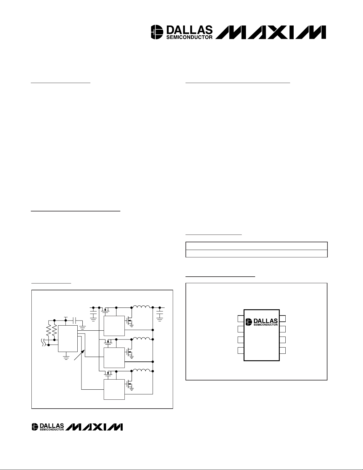
Ordering Information
V
OUT
V
IN
PHASE 1
PHASE 2
PHASE 3
DC-DC
STEP-DOWN
CONVERTER
OUT1
OUT2
OUT3
OUT4
GND
SCL
SDA
V
CC
V
CC
DS1094L
R
PULLUP
THREE-PHASE
EXAMPLE WITH
DITHERED CLOCKS TO
REDUCE EMI
DC-DC
STEP-DOWN
CONVERTER
DC-DC
STEP-DOWN
CONVERTER
Typical Operating Circuit
Rev 1; 5/04
For pricing, delivery, and ordering information, please contact Maxim/Dallas Direct! at
1-888-629-4642, or visit Maxim’s website at www.maxim-ic.com.
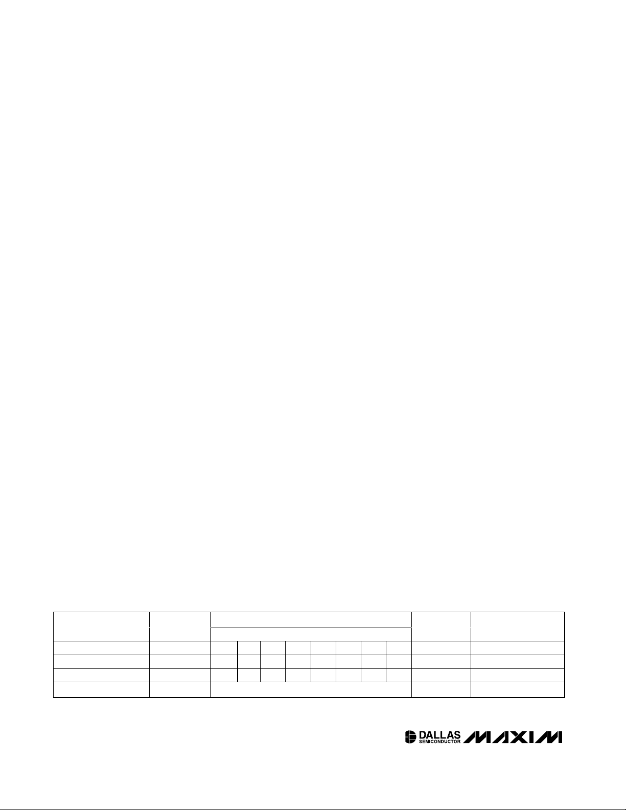
PART TEMP RANGE
PIN-PACKAGE
DS1094LU -40°C to +85°C 8 µSOP
EconOscillator is a trademark of Dallas Semiconductor.
I
2
C is a trademark of Philips Corp. Purchase of I2C components of Maxim Integrated Products, Inc., or one of its sublicensed Associated Companies, conveys a license under the
Philips I
2
C Patent Rights to use these components in an I2C
system, provided that the system conforms to the I
2
C Standard
Specification as defined by Philips.
Page 2
DS1094L
Multiphase Spread-Spectrum EconOscillator
2 _____________________________________________________________________
ABSOLUTE MAXIMUM RATINGS
RECOMMENDED DC OPERATING CONDITIONS
(TA= -40°C to +85°C)
Stresses beyond those listed under “Absolute Maximum Ratings” may cause permanent damage to the device. These are stress ratings only, and functional
operation of the device at these or any other conditions beyond those indicated in the operational sections of the specifications is not implied. Exposure to
absolute maximum rating conditions for extended periods may affect device reliability.
Voltage Range on VCC, SDA, and SCL
Relative to Ground.............................................-0.5V to +6.0V
Operating Temperature Range ...........................-40°C to +85°C
EEPROM Programming Temperature Range .........0°C to +70°C
Storage Temperature Range .............................-55°C to +125°C
Soldering Temperature .......................................See IPC/JEDEC
J-STD-020A Specification
PARAMETER
CONDITIONS
UNITS
Supply Voltage V
CC
(Note 1) 3.0 3.6 V
Input Logic 1 (SDA, SCL) V
IH
0.7 x
V
CC
+
0.3
V
Input Logic 0 (SDA, SCL) V
IL
+0.3 x
V
DC ELECTRICAL CHARACTERISTICS
(VCC= +3.0 to 3.6V, TA= -40°C to +85°C, unless otherwise noted.)
PARAMETER
CONDITIONS
UNITS
Active Supply Current I
CC
CL = 15pF per output, SDA = SCL = V
CC
1.4 3 mA
High-Level Output Voltage
(OUT1-4)
V
OH
IOH = -4mA; VCC = min 2.4 V
Low-Level Output Voltage
(OUT1-4)
V
OL
IOL = 3.5mA 0.4 V
3mA sink current 0.4
Low-Level Output Voltage (SDA)
V
OL
6mA sink current 0.6
V
High-Level Input Current
(SDA, SCL)
I
IH
VIH = V
CC
µA
Low-Level Input Current
(SDA, SCL)
I
IL
VIL = 0.0V
µA
SYMBOL
MIN TYP MAX
V
CC
SYMBOL
-0.3
MIN TYP MAX
-1.0
V
CC
+1.0
Page 3
DS1094L
Multiphase Spread-Spectrum EconOscillator
_____________________________________________________________________ 3
AC ELECTRICAL CHARACTERISTICS
(VCC= +3.0V to 3.6V, TA= -40°C to +85°C, unless otherwise noted.)
PARAMETER
CONDITIONS
UNITS
Master Oscillator Frequency f
MOSC
12
MHz
Output Frequency Tolerance ∆f
OUT
VCC = 3.3V,
T
A
= +25°C (Note 8)
%
Voltage Frequency Variation ∆f
OUT
TA = +25°C (Note 2)
%
0 to +70°C
Temperature Frequency Variation
∆f
OUT
-40°C to +85°C
%
DAC Step Size
%
Peak-to-Peak Jitter (3σ) P1:P0 = 11 (Note 3) 8 %
Load Capacitance C
L
15 50 pF
2 Phase 50
3 Phase
Output Duty Cycle (Note 4)
4 Phase 50
%
Power-Up Time
t
POR
+
t
STAB
(Note 5) 0.1 0.5 ms
AC ELECTRICAL CHARACTERISTICS (See Figure 3)
(VCC= +3.0V to 3.6V, TA= -40°C to +85°C, unless otherwise noted. Timing referenced to V
IL(MAX)
and V
IH(MIN)
.)
PARAMETER
SYMBOL
CONDITIONS
MIN
TYP
MAX
UNITS
SCL Clock Frequency f
SCL
(Note 6) 0 400 kHz
Bus Free Time Between Stop and
Start Conditions
t
BUF
1.3 µs
Hold Time (Repeated) Start
Condition
0.6 µs
Low Period of SCL t
LOW
1.3 µs
High Period of SCL t
HIGH
0.6 µs
Data Hold Time
0 0.9 µs
Data Setup Time
ns
Start Setup time t
SU:STA
0.6 µs
SDA and SCL Rise Time t
R
(Note 7)
20 +
300 ns
SDA and SCL Fall Time t
F
(Note 7)
20 +
300 ns
Stop Setup Time
0.6 µs
SDA and SCL Capacitive
Loading
C
B
(Note 7) 400 pF
EEPROM Write Time t
WR
510ms
Input Capacitance C
I
5pF
SYMBOL
VCC = 3.3V (Note 2)
MIN TYP MAX
-2.5 +2.5
-0.5 +0.5
-1.1 +1.1
-2.5 +1.1
-0.75 +0.75
33.3
t
HD:STA
t
HD:DAT
t
SU:DAT
t
SU:STO
100
0.1C
0.1C
B
B
Page 4
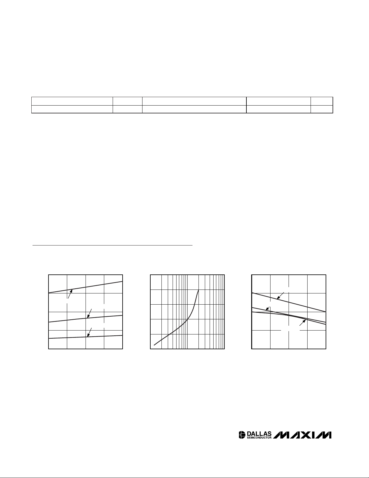
SUPPLY CURRENT vs. SUPPLY VOLTAGE
f
OUT
= 1MHz, 2φ MODE
DS1094L toc01
SUPPLY VOLTAGE (V)
SUPPLY CURRENT (mA)
3.453.303.15
0.75
1.00
1.25
1.50
0.50
3.00 3.60
TA = +85°C
TA = +25°C
TA = -40°C
SUPPLY CURRENT vs. FREQUENCY
V
CC
= 3.3V, 2φ MODE
DS1094L toc02
f
OUT
(MHz)
SUPPLY CURRENT (mA)
1.00
0.5
1.5
1.0
2.0
2.5
0
0.1 10.00
DUTY CYCLE vs. SUPPLY VOLTAGE
f
OUT
= 2MHz, 2φ MODE
DS1094L toc03
SUPPLY VOLTAGE (V)
DUTY CYCLE (%)
3.453.303.15
50.25
50.50
50.75
51.00
50.00
3.00 3.60
TA = +85°C
TA = +25°C
TA = -40°C
Typical Operating Characteristics
(VCC= +3.3V, TA = +25°C, unless otherwise noted.)
DS1094L
Multiphase Spread-Spectrum EconOscillator
4 _____________________________________________________________________
NONVOLATILE MEMORY CHARACTERISTICS
(VCC= +3.0V to 3.6V, unless otherwise noted.)
PARAMETER
CONDITIONS
UNITS
EEPROM Writes +70°C (Note 4)
Note 1: All voltages referenced to ground.
Note 2: This is the change observed in output frequency due to changes in temperature or voltage.
Note 3: This is a percentage of the output period. Parameter is characterized but not production tested. This can be varied from
2%, 4%, or 8%.
Note 4: This parameter is guaranteed by design.
Note 5: This indicates the time between power-up and the outputs becoming active. An on-chip delay is intentionally introduced to
allow the oscillator to stabilize. t
STAB
is equivalent to approximately 64 f
MOSC
cycles and, hence, will depend on the pro-
grammed clock frequency.
Note 6: Timing shown is for fast-mode (400kHz) operation. This device is also backward compatible with I
2
C standard-mode timing.
Note 7: CB—total capacitance of one bus line in picofarads.
Note 8: Typical frequency shift due to aging is ±0.5%. Aging stressing includes Level 1 moisture reflow preconditioning (24hr
+125°C bake, 168hr 85°C/85%RH moisture soak, and 3 solder reflow passes +240 +0/-5°C peak) followed by 1000hr max
V
CC
biased 125°C HTOL, 1000 temperature cycles at -55°C to +125°C, and 168hr 121°C/2 ATM Steam/Unbiased Autoclave.
SYMBOL
MIN TYP MAX
10,000
Page 5

DS1094L
Multiphase Spread-Spectrum EconOscillator
_____________________________________________________________________ 5
Typical Operating Characteristics (continued)
(VCC= +3.3V, TA = +25°C, unless otherwise noted.)
Pin Description
PIN
NAME
FUNCTION
1
Oscillator Output 1
2
Oscillator Output 2
3VCCPositive Supply Terminal
4 GND Ground
5
Oscillator Output 3
6
Oscillator Output 4
7 SDA
2-Wire Serial-Interface Data
Input/Output
8 SCL 2-Wire Serial-Interface Clock Input
DUTY CYCLE vs. FREQUENCY
= 3.3V, +25°C
V
55
50
45
40
DUTY CYCLE (%)
35
30
1.00 2.00
CC
φ
2
DS1094L toc04
φ
4
φ
3
1.751.501.25
f
(MHz)
OUT
TEMPERATURE FREQUENCY VARIATON
0.4
0
-.04
-0.8
ERROR (%)
-1.2
-1.6
f
OUT
= 125kHz
f
OUT
f
OUT
ERROR (%)
OUTPUT FREQUENCY TOLERANCE
= 3.3V, +25°C
V
DS1094L toc07
CC
1.751.501.25
f
(MHz)
OUT
0.5
0
-0.5
-1.0
-1.5
1.00 2.00
= 2MHz
= 1MHz
2.5
2.0
1.5
JITTER (%)
1.0
VOLTAGE FREQUENCY VARIATION
0.50
DS1094L toc05
0.25
0
ERROR (%)
-0.25
-0.50
3.0 3.6
SUPPLY VOLTAGE (V)
PEAK-TO-PEAK JITTER vs. f
f
OUT
f
OUT
f
OUT
= 125kHz
MOSC
= 1MHz
= 2MHz
DS1094L toc06
3.53.03.2
DS1094L toc08
-2.0
-40 85
TEMPERATURE (°C)
OUT1
OUT2
OUT3
OUT4
0.8
603510-15
1.0 2.0
f
(MHz)
MOSC
1.81.61.41.2
Page 6

DS1094L
Detailed Description
The DS1094L consists of a master oscillator, prescaler,
phase generator, and triangle-wave generator (used to
dither the master oscillator), which are all programmable using the 2-wire interface and stored in NV memory.
Master Oscillator
The master oscillator is responsible for generating the
timing (frequency) of the outputs. The master oscillator
frequency, f
MOSC
, can be programmed anywhere
between 1MHz to 2MHz in 100kHz steps. The master
oscillator is programmed using the DAC register. The four
MSBs of the DAC register are don’t cares, while the four
LSBs (D3 to D0) are the DAC value. The master oscillator
frequency is determined using the following equation:
f
MOSC
= 1MHz + (DAC value x 100kHz)
Valid values for DAC are 0 to 10 (dec). DAC values
greater than 10 exceed the 2MHz limit and are not permitted.
The master oscillator also determines the spread-spectrum dither frequency. This is described in the Triangle
Wave Generator section.
Multiphase Spread-Spectrum EconOscillator
6 _____________________________________________________________________
GND
MASTER
OSCILLATOR
1MHz TO 2MHz
PRESCALER
DIVIDE BY
1, 2, 4, OR 8
TRIANGLE
WAVE
GENERATOR
2-WIRE
SERIAL
INTERFACE
TWO/THREE/
FOUR-PHASE
GENERATOR
DAC
PRESCALER
ADDR
D0D1D2D3XXXX
P0P1J0J1PH0PH1D0D1
A0A1A2WCXXXX
V
CC
V
CC
SCL
SDA
DITHER RATE
DITHER %
EEPROM
WRITE EE
COMMAND
OUT2
OUT1
OUT3
OUT4
2-WIRE ADDRESS BITS
PHASE SELECTPRESCALER SETTING
EEPROM WRITE CONTROL
CONTROL REGISTERS
DAC SETTING
f
MOSC
f
OSC
f
MOSC
f
MOD
f
OUT
DS1094L
Functional Diagram
DAC VALUE (dec)
DAC REGISTER
f
MOSC
0 00h 1.0MHz
1 01h 1.1MHz
2 02h 1.2MHz
———
10 0Ah 2.0MHz
11 to 15 0Bh to 0Fh Reserved
Table 1. Master Oscillator Settings
BITS P1, P0 DIVISOR f
OSC
=
00 2
0
f
MOSC
/1
01 2
1
f
MOSC
/2
10 2
2
f
MOSC
/4
11 2
3
f
MOSC
/8
Table 2. Prescaler Settings
Page 7

Prescaler
The prescaler divides the master oscillator frequency,
f
MOSC
, by 1, 2, 4, or 8. The resultant frequency, f
OSC
, is
calculated using the following formula:
f
OSC
= f
MOSC
/ 2
PRESCALER
where PRESCALER can be 0 to 3. The prescaler is configured using bits P1 and P0 in the PRESCALER register. Valid settings are shown in Table 2. The location of
bits P1 and P0 in the PRESCALER register is shown in
the Control Registers section.
Note that the PRESCALER register also contains bits
controlling other features of the device (dither amount,
dither rate, and phase).
Phase Generator
The four oscillator outputs (OUT1 to OUT4) can be configured in either two-phase, three-phase, or four-phase
mode. The output waveforms of each mode are illustrated in Figure 1. Likewise, the figure also shows a
comparison of f
OUT
, the duty cycle, and the output
phase shifts between the three modes. Bits Ph1 and
Ph0 in the PRESCALER register are used to select the
desired mode (see Table 3). The location of bits Ph1
and Ph0 in the PRESCALER register is shown in the
Control Registers section.
Triangle Wave Generator
The triangle wave generator is used to dither the master oscillator frequency, adding spread-spectrum functionality to the DS1094L by injecting an offset element
into the master oscillator. Both the dither amount (%)
and dither frequency are programmable. The dither
amount is controlled by bits J1 and J0 in the
PRESCALER register. The dither frequency is controlled by bits D1 and D0, also in the PRESCALER register. The bit settings are shown in Table 4 and 5. The
location of bits J1, J0, D1, and D0 in the PRESCALER
register is shown in the Control Registers section.
When dither is enabled (by selecting a percentage
other than 0%), the master oscillator frequency, f
MOSC
,
is dithered between the programmed f
MOSC
and the
selected percentage down from the programmed
f
MOSC
(see Figure 2). For example, if f
MOSC
is programmed to 2MHz (DAC register = 0Ah) and the dither
amount is programmed to 2%, the frequency of f
MOSC
DS1094L
Multiphase Spread-Spectrum EconOscillator
_____________________________________________________________________ 7
BITS Ph1, Ph0 MODE
00 Two-Phase
01 Three-Phase
10 Four-Phase
11 Reserved
Table 3. Phase Generator Settings
BITS J1, J0 DITHER AMOUNT*
00 0%
01 2%
10 4%
11 8%
Table 4. Dither Amount Settings
BITS D1, D0 DITHER FREQUENCY
00 f
MOSC
/128
01 f
MOSC
/256
10 f
MOSC
/512
11 f
MOSC
/1024
Table 5. Dither Frequency Settings
OUT1
OUT2
OUT3
OUT4
OUT1
OUT2
OUT3
OUT4
OUT1
OUT2
OUT3
OUT4
f
OSC
TWO-PHASE
THREE-PHASE
FOUR-PHASE
50% DUTY CYCLE
50% DUTY CYCLE
33% DUTY CYCLE
120 DEGREES
OUT OF PHASE
180 DEGREES
90 DEGREES OUT
OF PHASE
f
OUT
= f
OSC
OUT OF PHASE
f
OUT
= f
OSC
/ 3
f
OUT
= f
OSC
/ 4
Figure 1. DS1094L Output Waveforms
TIME
1
DITHER FREQ.
PROGRAMMED f
MOSC
PROGRAMMED f
MOSC
-
(2, 4, OR 8% OF f
MOSC
)
DITHER
AMOUNT
(2, 4, OR 8%)
IF DITHER AMOUNT = 0%
f
MOSC
Figure 2. DS1094L Dither Waveform
*The frequency is dithered down from the programmed value
of f
MOSC
.
Page 8
DS1094L
will dither between 2MHz and 1.96MHz at a modulation
frequency determined by the selected dither frequency. Continuing with the same example, if D1 and D0
both equal zero, selecting f
MOSC
/128, then the dither
frequency would be 15.625kHz.
2-Wire Slave Address
The 2-wire serial interface is used to read and write the
control registers of the DS1094L. The default slave
address of the DS1094L is B0h (see Figure 4). Using
the 3 address bits (A2, A1, and A0) in the ADDR register, the slave address can be changed to allow as
many as eight DS1094Ls reside on the same 2-wire
bus or to simply prevent address conflicts with other 2wire devices. The location of the address bits within the
ADDR register is shown in the Control Registers section. A detailed description of the 2-wire interface is
found in the 2-Wire Serial Interface Description section.
EEPROM Write Control
Since EEPROM does have a limited number of lifetime
write cycles (specified in the NONVOLATILE MEMORY
CHARACTERISTICS electrical table), it is possible to
configure the DS1094L to prevent EEPROM wear out
and eliminate the EEPROM write cycle time by using
the WC bit in the ADDR register. When the WC bit is 0
(default), register writes are automatically written into
EEPROM. The Write EE Command is not needed.
However, if WC = 1, then register writes are stored in
SRAM and only written to EEPROM when the user
sends the Write EE Command. If power to the device is
cycled, the last value stored in EEPROM is recalled.
The time required to store the values is one EEPROM
write cycle time. WC = 1 is ideal for applications that
frequently modify the frequency/registers.
Regardless of the value of the WC bit, the value of the
ADDR register is always written immediately to EEPROM.
Control Registers
The DS1094L control registers are used to program the
frequency and features of the device. Table 6 lists the
DS1094L’s control registers and illustrates bit locations
as well as other valuable information. The memory
address of each register is shown in the ADDRESS column. The factory default values programmed into EEPROM are shown in the DEFAULT column. Refer to the
corresponding sections to determine what values to
write to the registers.
PRESCALER (02h)
D1, D0 Selects the dither frequency. Refer to Table 5.
Ph1, Ph0 Determines whether the two-phase, three-
phase, or four-phase mode is selected. Refer
to Table 3.
J1, J0 Selects the dither amount. Refer to Table 4.
P1, P0 Determines the prescaler value. Refer to
Table 2.
DAC (08h)
D3 to D0 This four-bit value determines the master oscil-
lator frequency, f
MOSC
. Refer to Table 1 and
the Master Oscillator section for a detailed
information on calculating the DAC value.
ADDR (0Dh)
WC The EEPROM write control bit determines if
writes to control registers are automatically
backed up in NV memory (EEPROM) or
whether a write EE command is required to
write to NV memory. See the EEPROM Write
Control section for more information.
A2 to A0 This three-bit value determines the 2-wire
slave address.
WRITE EE COMMAND (3Fh)
This command can be used when the WC bit = 1 (see
explanation in the EEPROM Write Control section) to
transfer registers internally from SRAM to EEPROM. The
time required to store the values is one EEPROM write
cycle time. This command is not needed if WC = 0.
Multiphase Spread-Spectrum EconOscillator
8 _____________________________________________________________________
BINARY
REGISTER
MSB
ACCESS
PRESCALER 02h
R/W
DAC 08h
R/W
ADDR 0Dh
R/W
WRITE EE Command
3Fh No Data W
Table 6. Control Registers
X = Don’t care
X
1
= Don’t care, reads as 1
ADDRESS
LSB
D1 D0 Ph1 Ph0 J1 J0 P1 P0 11001101b
X1X1X1X1D3 D2 D1 D0 XXXX0000b
X1X1X1X1WC A2 A1 A0 XXXX0000b
DEFAULT
Page 9

2-Wire Serial Interface
Description
Definitions
The following terminology is commonly used to
describe 2-wire data transfers.
Master Device: The master device controls the slave
devices on the bus. The master device generates SCL
clock pulses, start, and stop conditions.
Slave Devices: Slave devices send and receive data
at the master’s request.
Bus Idle or Not Busy: Time between stop and start
conditions when both SDA and SCL are inactive and in
their logic high states. When the bus is idle it often initiates a low-power mode for slave devices.
Start Condition: A start condition is generated by the
master to initiate a new data transfer with a slave.
Transitioning SDA from high to low while SCL remains
high generates a start condition. See the timing diagram for applicable timing.
Stop Condition: A stop condition is generated by the
master to end a data transfer with a slave. Transitioning
SDA from low to high while SCL remains high generates a stop condition. See the timing diagram for
applicable timing.
Repeated Start Condition: The master can use a
repeated start condition at the end of one data transfer
to indicate that it will immediately initiate a new data
transfer following the current one. Repeated starts are
commonly used during read operations to identify a
specific memory address to begin a data transfer. A
repeated start condition is issued identically to a normal start condition. See the timing diagram for applicable timing.
Bit Write: Transitions of SDA must occur during the low
state of SCL. The data on SDA must remain valid and
unchanged during the entire high pulse of SCL plus the
setup and hold time requirements (see Figure 3). Data is
shifted into the device during the rising edge of the SCL.
Bit Read: At the end of a write operation, the master
must release the SDA bus line for the proper amount of
setup time (see Figure 3) before the next rising edge of
SCL during a bit read. The device shifts out each bit of
data on SDA at the falling edge of the previous SCL
pulse, and the data bit is valid at the rising edge of the
current SCL pulse. Remember that the master generates all SCL clock pulses including when it is reading
bits from the slave.
Acknowledgement (ACK and NACK): An
Acknowledgement (ACK) or Not Acknowledge (NACK) is
always the 9th bit transmitted during a byte transfer. The
device receiving data (the master during a read or the
slave during a write operation) performs an ACK by
transmitting a zero during the 9th bit. A device performs
a NACK by transmitting a one during the 9th bit. Timing
(Figure 3) for the ACK and NACK is identical to all other
bit writes. An ACK is the acknowledgement that the
device is properly receiving data. A NACK is used to terminate a read sequence or as an indication that the
device is not receiving data.
Byte Write: A byte write consists of 8 bits of information
transferred from the master to the slave (most significant
bit first) plus a 1-bit acknowledgement from the slave to
the master. The 8 bits transmitted by the master are
done according to the bit write definition, and the
acknowledgement is read using the bit read definition.
Byte Read: A byte read is an 8-bit information transfer
from the slave to the master plus a 1-bit ACK or NACK
from the master to the slave. The 8 bits of information
DS1094L
Multiphase Spread-Spectrum EconOscillator
_____________________________________________________________________ 9
SDA
SCL
t
HD:STA
t
LOW
t
HIGH
t
R
t
F
t
BUF
t
HD:DAT
t
SU:DAT
REPEATED
START
t
SU:STA
t
HD:STA
t
SU:STO
t
SP
STOP
NOTE: TIMING IS REFERENCED TO V
IL(MAX)
AND V
IH(MIN)
.
START
Figure 3. 2-Wire Timing Diagram
Page 10

DS1094L
that are transferred (most significant bit first) from the
slave to the master are read by the master using the bit
read definition above, and the master transmits an ACK
using the bit write definition to receive additional data
bytes. The master must NACK the last byte read to terminate communication so the slave will return control of
SDA to the master.
Slave Address Byte: The slave address byte consists of
a 7-bit slave address followed by the R/W bit (see Figure
4). The slave address is the most significant 7 bits and
the R/W bit is the least significant bit. The 3 address bits
in the slave address (A2 to A0) permit a maximum of
eight DS1094Ls to share the same 2-wire bus.
Each slave on the 2-wire bus has a unique slave
address, which is used by the master to select which
slave it wishes to communicate with. Following a start
condition, all slaves on the 2-wire bus await the slave
address byte from the master. Each slave compares its
own slave address with the slave address sent from the
master. If the slave address matches, the slave
acknowledges and continues communication with the
master (based on the R/W bit). Otherwise, if the slave
address does not match, the slave ignores communication until the next start condition.
When the R/W bit is zero, the master writes data to the
specified slave. When the R/W is one, the master reads
data from the specified slave.
Memory Address: During a 2-wire write operation, the
master must transmit a memory address to identify the
memory location where the slave is to store the data.
The memory address is always the second byte transmitted during a write operation following the slave
address byte (R/W = 0).
2-Wire Communication
Writing a Single Byte to a Slave: The master must
generate a start condition, write the slave address byte
(with R/W = 0), write the memory address, write the
byte of data, and generate a stop condition. The master
must read the slave’s acknowledgement following each
byte write.
Acknowledge Polling: Any time EEPROM is written,
the EEPROM write time (t
W
) is required following the
stop condition to write to EEPROM. During the EEPROM write time, the DS1094L will not acknowledge its
slave address because it is busy. It is possible to take
advantage of this phenomenon by repeatedly addressing the DS1094L until it finally acknowledges its slave
address. The alternative to acknowledge polling is to
wait for maximum period of tWto elapse before
attempting to write to EEPROM again.
Reading a Single Byte from a Slave: A dummy write
cycle is used to read a particular register. To do this
the master generates a start condition, writes the slave
address byte (with R/W = 0), writes the memory
address of the desired register to read, generates a
repeated start condition, writes the slave address byte
(with R/W = 1), reads the register and follows with a
NACK (since only one byte is read), and generates a
stop condition. See Figure 5 for examples of reading
DS1094L registers.
Application Information
SDA and SCL Pullup Resistors
SDA is an open-collector output and requires a pullup
resistor to realize high logic levels. Because the
DS1094L does not utilize clock cycle stretching, a master using either an open-collector output with a pullup
resistor or CMOS output driver (push-pull) can be utilized for SCL. Pullup resistor values should be chosen
to ensure that the rise and fall times listed in the AC
electrical characteristics are within specification.
Stand-Alone Operation
If the DS1094L is used stand-alone (without a 2-wire
master), SDA and SCL should not be left unconnected,
or floating. It is recommended that pullup resistors be
used on both SDA and SCL to prevent the pins from
floating to unknown voltages and transitions. Likewise,
pullups are recommended over tying SDA and SCL
directly to VCCto allow future programmability.
Power-Supply Decoupling
To achieve best results, it is highly recommended that
a decoupling capacitor is used on the IC power supply
pins. Typical values of decoupling capacitors are
0.01µF and 0.1µF. Use high-quality, ceramic, surfacemount capacitors. Mount the capacitors as close as
possible to the VCCand GND pins of the IC to minimize
lead inductance.
Multiphase Spread-Spectrum EconOscillator
10 ____________________________________________________________________
R/WA0*A1*A2*1101
MSB LSB
*THESE BITS MUST MATCH THE
CORRESPONDING BITS IN THE ADDR REGISTER.
7-BIT SLAVE ADDRESS READ/WRITE BIT
Figure 4. Slave Address Byte
Page 11

DS1094L
Multiphase Spread-Spectrum EconOscillator
Maxim cannot assume responsibility for use of any circuitry other than circuitry entirely embodied in a Maxim product. No circuit patent licenses are
implied. Maxim reserves the right to change the circuitry and specifications without notice at any time.
Maxim Integrated Products, 120 San Gabriel Drive, Sunnyvale, CA 94086 408-737-7600 ____________________ 11
© 2004 Maxim Integrated Products Printed USA is a registered trademark of Maxim Integrated Products.
DALLAS is a registered trademark of Dallas Semiconductor Corporation.
Chip Topology
TRANSISTOR COUNT: 7987
SUBSTRATE CONNECTED TO: GROUND
Package Information
For the latest package outline information, go to
www.maxim-ic.com/DallasPackInfo.
SLAVE ADDRESS
START 1 0 1 1 A2* A1* A0*
R/W
SLAVE
ACK
SLAVE
ACK
SLAVE
ACK
SLAVE
ACK
SLAVE
ACK
SLAVE
ACK
SLAVE
ACK
SLAVE
ACK
SLAVE
ACK
SLAVE
ACK
SLAVE
ACK
SLAVE
ACK
SLAVE
ACK
SLAVE
ACK
MSB LSB
b7 b6 b5 b4 b3 b2 b1 b0
MSB LSB
READ/
WRITE
COMMAND/REGISTER ADDRESS
b7 b6 b5 b4 b3 b2 b1 b0
MSB LSB
DATA
STOP
A) SINGLE BYTE WRITE
-WRITE DAC REGISTER TO 0Ah
C) SINGLE BYTE WRITE
-WRITE PRESCALER
REGISTER TO CDh
B) SINGLE BYTE READ
-READ DAC REGISTER
D) WRITE EE COMMAND
- NEEDED ONLY IF WC = 1
TYPICAL 2-WIRE WRITE TRANSACTION
START STOP10110000 00111 111
B0h 3Fh
START
REPEATED
START
B1h
MASTER
NACK
STOP10110000 00001 000
B0h 08h
10110001
START 1 0 1 1 0 000 00001 000
B0h 08h
STOP
DAC VALUE
START 1 0 1 1 0 000 00000 010
B0h 02h
STOP
DATA
CDh
0Ah
EXAMPLE 2-WIRE TRANSACTIONS (WHEN A0, A1, AND A2 ARE ZERO)
* THE ADDRESS DETERMINED BY A0, A1, AND A2 MUST MATCH THE ADDRESS SET IN THE ADDR REGISTER.
00001 010
11001 101
Figure 5. 2-Wire Communication Examples
 Loading...