

Page 1
General Description
The DS1091L is a low-cost clock generator that is factorytrimmed to output frequencies from 130kHz to 66.6MHz
with a nominal accuracy of ±0.25%. The device can also
produce a center- or down-dithered spread-spectrum
output with pin-selectable dither magnitude and rate.
Assembled in an 8-pin µMAX package, the DS1091L is
designed to operate with a 3.0V to 3.6V power supply
over the automotive temperature range (-40°C to
+125°C).
Applications
Automotive Infotainment
POS Terminals
LCD Displays
Printers
Industrial Control
Features
♦ Spread-Spectrum Clock Output from 130kHz to
66.6MHz
♦ Operating Temperature Range of -40°C to +125°C
♦ Accuracy of ±1.75% Across Temperature and
Voltage
♦ Factory Trimmed
♦ Center-Dithered (DS1091LA) or Down-Dithered
(DS1091LB) Spread-Spectrum Output
♦ Pin-Selectable Center-Dither Magnitude of 0%,
±1%, ±2%, or ±4%
♦ Pin-Selectable Down-Dither Magnitude of 0%, -2%,
-4%, or -8%
♦ Pin-Selectable Dither Rate
♦ 3.0V to 3.6V Supply Operation
♦ Lead-Free 8-Pin µMAX Package
DS1091L
Automotive Temperature Range
Spread-Spectrum Econoscillator
______________________________________________
Maxim Integrated Products
1
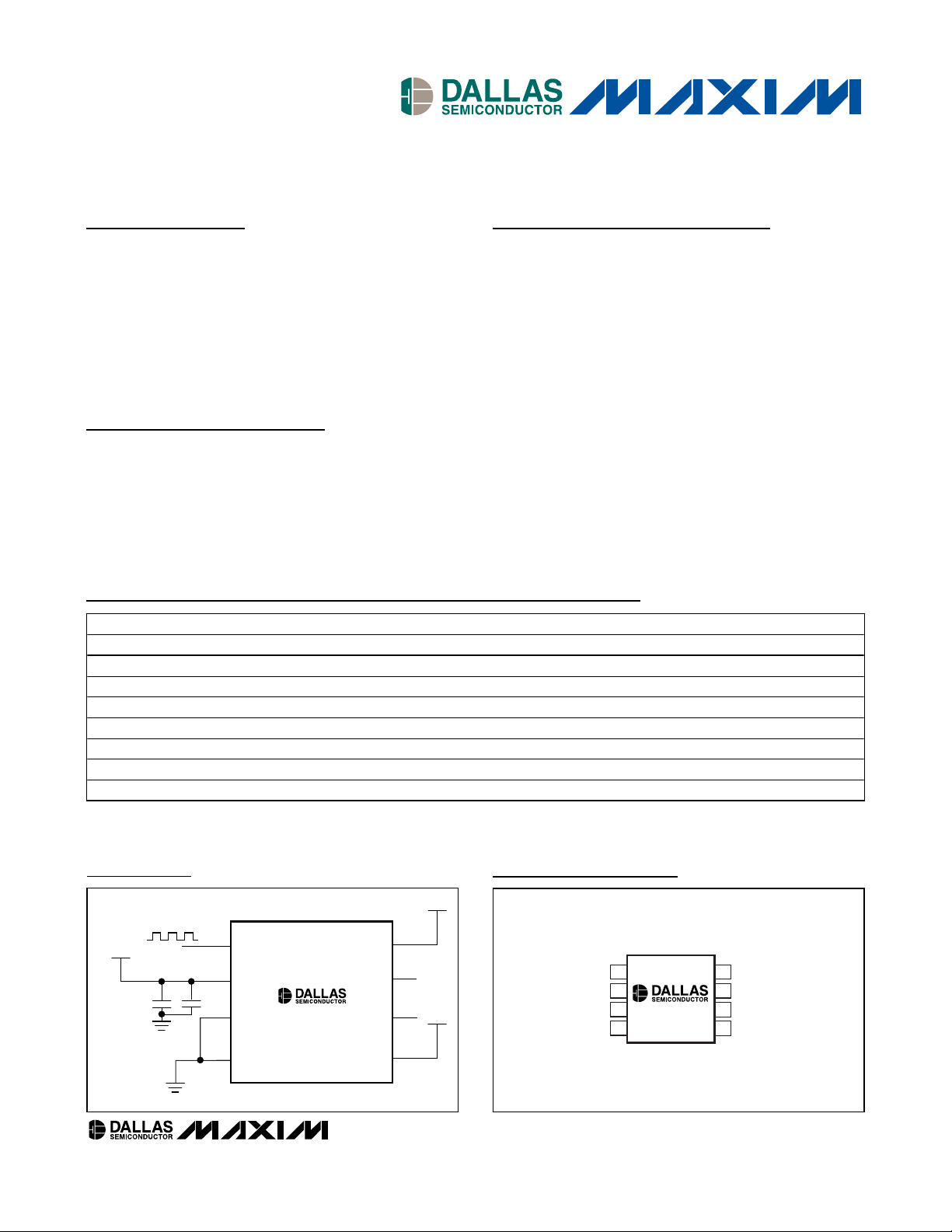
Pin Configuration
8
3
4
2
1
OUT
DR
8 μMAX
DS1091L
V
CC
V
CC
f
OUT
DECOUPLING
CAPACITORS
7
6
5
SEL0
V
CC
N.C.
N.C.
SEL1
GND
V
CC
Typical Operating Circuit
Rev 0; 9/06
For pricing, delivery, and ordering information, please contact Maxim/Dallas Direct! at
1-888-629-4642, or visit Maxim’s website at www.maxim-ic.com.
+
Denotes lead-free package.
xxx
Denotes factory-programmed custom frequencies.
Email Custom_EconOscillators_Info@dalsemi.com for information/questions concerning custom frequencies.
Ordering Information
µMAX
8 µMAX
PART TEMP RANGE PIN-PACKAGE SPREAD SPECTRUM OUTPUT FREQUENCY (MHz)
DS1091LUA+027 -40°C to +125°C 8 µMAX Center 27.0
DS1091LUA+033 -40°C to +125°C 8 µMAX Center 33.3
DS1091LUA+066 -40°C to +125°C 8 µMAX Center 66.6
DS1091LUA+xxx -40°C to +125°C 8 µMAX Center Custom (Contact Factory)
DS1091LUB+027 -40°C to +125°C 8 µMAX Down 27.0
DS1091LUB+033 -40°C to +125°C 8 µMAX Down 33.3
DS1091LUB+066 -40°C to +125°C 8 µMAX Down 66.6
DS1091LUB+xxx -40°C to +125°C 8 µMAX Down Custom (Contact Factory)
TOP VIEW
1
OUT
2
V
CC
3
GND
4
8
DR
7
N.C.
6
DS1091L
μMAX
N.C.
5
SEL0SEL1
Page 2
ABSOLUTE MAXIMUM RATINGS
RECOMMENDED OPERATING CONDITIONS
(TA= -40°C to +125°C.)
Stresses beyond those listed under “Absolute Maximum Ratings” may cause permanent damage to the device. These are stress ratings only, and functional
operation of the device at these or any other conditions beyond those indicated in the operational sections of the specifications is not implied. Exposure to
absolute maximum rating conditions for extended periods may affect device reliability.
Voltage on VCCRelative to Ground.......................-0.5V to +6.0V
Voltage on DR, SEL0, SEL1 Relative
to Ground*..............................................-0.5V to (V
CC
+ 0.5V)
Operating Temperature Range .........................-40°C to +125°C
Storage Temperature Range .............................-55°C to +125°C
Soldering Temperature...................See J-STD-020 Specification
DC ELECTRICAL CHARACTERISTICS
(TA= -40°C to +125°C; VCC= +3.0V to +3.6V, unless otherwise noted.)
*
This voltage must not exceed 6.0V.
AC ELECTRICAL CHARACTERISTICS
(TA= -40°C to +125°C; VCC= +3.0V to +3.6V, unless otherwise noted.)
DS1091L
Automotive Temperature Range
Spread-Spectrum Econoscillator
2 _____________________________________________________________________
PARAMETER SYMBOL CONDITIONS MIN TYP MAX UNITS
Supply Voltage V
High-Level Input Voltage
(SEL0, SEL1, DR)
Low-Level Input Voltage
(SEL0, SEL1, DR)
V
V
(Note 1) 3.0 3.3 3.6 V
CC
IH
IL
0.7 x
V
CC
-0.3
V
CC
0.3
0.3 x
V
+
CC
V
V
High-Level Output Voltage (OUT) V
Low-Level Output Voltage (OUT) V
High-Level Input Current
(SEL0, SEL1, DR)
Low-Level Input Current
(SEL0, SEL1, DR)
Supply Current (Active) I
PARAMETER SYMBOL CONDITIONS MIN TYP MAX UNITS
OHIOH
OL
I
IH
I
IL
CC
= -4mA, VCC = 3.0V 2.4 V
IOL = 4mA 0.4 V
VCC = 3.6V 1 µA
VIL = 0 -1 µA
(Note 2) 16 mA
Output Frequency Range f
Power-Up Time t
Load Capacitance C
PARAMETER SYMBOL CONDITIONS MIN TYP MAX UNITS
OUT
(Note 3) 0.130 66.6 MHz
VCC = 3.3V, TA = +25°C -0.25 0 +0.25
Across TA and V
OUT
0°C to +70°C, across V
(Note 4) 0.1 ms
PU
L
CC
CC
-1.75 +1.75Output Center Frequency Tolerance Δf
-1.2 +1.2
15 50 pF
%
Page 3

DS1091L
Automotive Temperature Range
Spread-Spectrum Econoscillator
_____________________________________________________________________ 3
Note 1: All voltages are referenced to ground. Currents entering the IC are specified positive and currents exiting the IC are negative.
Note 2: Supply current measured with C
L
= 15pF, VCC= 3.6V, TA = 25°C, f
OUT
= 66.6MHz, no dither.
Note 3: No dither.
Note 4: Guaranteed by design.
Note 5: For aging characteristics, contact factory.
Typical Operating Characteristics
(TA= +25°C, VCC= 3.3V, unless otherwise noted.)
AC ELECTRICAL CHARACTERISTICS (continued)
(TA= -40°C to +125°C; VCC= +3.0V to +3.6V.)
Duty Cycle
Jitter (RMS), 50MHz 0.3 %
PARAMETER SYMBOL CONDITIONS MIN TYP MAX UNITS
< 33.3MHz (Note 3) 50
≥ 33.3MHz (Note 3) 40 60
%
ICC vs. TEMPERATURE
9.2
9.0
8.8
8.6
8.4
(mA)
CC
I
8.2
8.0
7.8
7.6
7.4
-40 20-10 50 80 110
VCC = 3.6V
VCC = 3.3V
VCC = 3.0V
TEMPERATURE (°C)
1.75
1.25
DS1091L toc01
0.75
0.25
-0.25
-0.75
FREQUENCY VARIATION (%)
-1.25
-1.75
-40 20 50-10 80 110
FREQUENCY VARIATION (%)
vs. TEMPERATURE
VCC = 3.3V
NO DITHER
f
= 130kHz
OUT
f
= 66MHz
OUT
TEMPERATURE (°C)
0.25
0.20
DS1091L toc02
0.15
0.10
0.05
0.00
-0.05
-0.10
FREQUENCY VARIATION (%)
-0.15
-0.20
-0.25
FREQUENCY VARIATION (%)
vs. VOLTAGE
f
= 66MHz
OUT
f
= 130kHz
OUT
NO DITHER
3.0 3.23.1 3.3 3.4 3.5 3.6
VCC (V)
DS1091L toc03
DUTY CYCLE vs. V
52.0
51.5
f
= 66MHz
51.0
50.5
50.0
49.5
DUTY CYCLE (%)
49.0
48.5
48.0
3.0 3.23.1 3.3 3.4 3.5 3.6
OUT
f
OUT
VCC (V)
= 130kHz
NO DITHER
CC
DS1091L toc04
DUTY CYCLE (%)
DUTY CYCLE vs. TEMPERATURE
60
58
56
54
52
50
48
46
44
42
40
-40 -15 10 35 60 85 110
f
= 66MHz
OUT
f
= 130kHz
OUT
TEMPERATURE (°C)
NO DITHER
DS1091L toc05
Page 4

DS1091L
Automotive Temperature Range
Spread-Spectrum Econoscillator
4 _____________________________________________________________________
Typical Operating Characteristics (continued)
(TA= +25°C, VCC= 3.3V, unless otherwise noted.)
Pin Description
PIN
µMAX8
NAME FUNCTION
1 OUT Spread-Spectrum Clock Output
2VCCSupply Voltage
3 GND Ground
4 SEL1
5 SEL0
Spread Spectrum Dither Magnitude Select Inputs. Selects dither magnitude (see Table 1).
6, 7 N.C. No Connection
8 DR Spread-Spectrum Dither Rate Selector. Selects dither rate (see Table 2).
0.0
0.5
1.0
1.5
2.0
2.5
3.0
3.5
OUTPUT FALL TIME
DS1091L toc07
TIME (ns)
OUTPUT (V)
FALL TIME
= 1.13ns
TYPICAL
AT 12pF LOAD
-35
-30
-25
-20
-15
-10
-5
0
5
31.9 32.932.4 33.4 33.9 34.4
34.9
SPECTRUM ATTENUATION vs. FREQUENCY
AT DIFFERENT DITHER AMPLITUDES
DS1091L toc08
FREQUENCY (MHz)
ATTENUATION (dB)
0%
±1%
±2%
±4%
8dB
11dB
14dB
f
OUT
= 33.3MHz
RBW = 120kHz
CENTER DITHER
0.0
0.5
1.0
1.5
2.0
2.5
3.0
3.5
OUTPUT RISE TIME
DS1091L toc06
TIME (ns)
OUTPUT (V)
RISE TIME
= 1.02ns
TYPICAL
AT 12pF LOAD
Page 5

Detailed Description
The DS1091L is a clock generator that is capable of
output frequencies from 130kHz to 66.6MHz over the
full automotive temperature range (-40°C to +125°C).
The device also is capable of producing a spreadspectrum (dithered) square-wave output using four pinselectable dither percentages. Both center (DS1091LA)
and down (DS1091LB) dithering options are available.
The device also features two selectable dither rates.
The DS1091L is shipped from the factory programmed
to a customer-specified frequency.
Spread Spectrum
The DS1091L has the ability to reduce radiated emission peaks. The dither percentage is controlled by the
state of the SEL0 and SEL1 pins. The output frequency
can be dithered at 0%, ±1%, ±2%, and ±4%, centered
around the programmed frequency (for the DS1091LB
this can be down dithered by 0%, -2%, -4%, and -8%).
The two select pins SEL0 and SEL1 provide a means of
selecting the dither magnitudes as follows:
A triangle wave generator injects a control signal into
the master oscillator to dither its output. The dither rate
is a function of the output frequency, f
OUT
as well as the
setting of the DR pin (see the equation below). Figure 1
shows a plot of the output frequency versus time.
where n is defined in Table 2 as a function of output frequency. For example, for an output frequency of
27.0MHz, the dither rate would be 13.2kHz for DR = 0
and 6.6kHz for DR = 1.
DS1091L
Automotive Temperature Range
Spread-Spectrum Econoscillator
_____________________________________________________________________ 5
Block Diagram
Table 1.
Table 2.
DS1091L
V
V
CC
GND
WHERE f
CC
DITHER RATE DIVIDER
IS THE MASTER OSCILLATOR FREQUENCY.
MOSC
FACTORY-PROGRAMMED
MASTER OSCILLATOR
f
MOSC
TRIANGLE WAVE GENERATOR
f
OUT
DITHER RATE
=
2
n
f
MOSC
f
OUT
(max)
OUT
OUT
DITHER MAGNITUDE
DS1091LA DS1091LB
n
DR = LOGIC
LEVEL 1
DR = LOGIC
LEVEL 0
f
DITHER
PRESCALER
(DITHER %)
SEL0SEL1DR
FACTORY-PROGRAMMED
SEL1
LOGIC LEVEL
0 0 No Dither No Dither
0 1 ±1% -2%
1 0 ±2% -4%
1 1 ±4% -8%
SEL0
LOGIC LEVEL
OUTPUT FREQUENCY f
(MHz)
f
(min) f
OUT
0.130 0.260 4 5
0.261 0.521 5 6
0.522 1.042 6 7
1.043 2.083 7 8
2.084 4.167 8 9
4.168 8.333 9 10
8.334 16.667 10 11
16.668 33.333 11 12
33.334 66.667 12 13
OUT
Page 6

DS1091L
Automotive Temperature Range
Spread-Spectrum Econoscillator
Maxim cannot assume responsibility for use of any circuitry other than circuitry entirely embodied in a Maxim product. No circuit patent licenses are
implied. Maxim reserves the right to change the circuitry and specifications without notice at any time.
6
_____________________Maxim Integrated Products, 120 San Gabriel Drive, Sunnyvale, CA 94086 408-737-7600
© 2006 Maxim Integrated Products is a registered trademark of Maxim Integrated Products, Inc.
is a registered trademark of Dallas Semiconductor Corporation.
Springer
Power-Up
Upon the application of power, the DS1091L output is
held in the low state until t
PU
has elapsed. This
removes any possibility of erroneous output transitions
during initial power-up.
DS1091L Frequency Spreading Profile as a
Function of Dither %
Application Information
Power-Supply Decoupling
To achieve best results, it is highly recommended that
decoupling capacitors are used on the IC power-supply
pins. Typical values of decoupling capacitors are 0.01µF
and 0.1µF. Use a high-quality, ceramic, surface-mount
capacitor, and mount it as close as possible to the V
CC
and GND pins of the IC to minimize lead inductance.
Requesting Custom Frequencies
Email Custom_EconOscillators_Info@dalsemi.com for
information/questions concerning custom frequencies.
Chip Topology
TRANSISTOR COUNT: 4887
SUBSTRATE CONNECTED TO GROUND
Package Information
For the latest package outline information, go to
www.maxim-ic.com/DallasPackInfo
.
Figure 1B. Down Dithered
Figure 1A. Center Dithered
PROGRAMMED f
(1%, 2%, OR 4% OF f
PROGRAMMED f
PROGRAMMED f
(1%, 2%, OR 4% OF f
OUT
OUT
OUT
OUT
OUT
+
)
)
OUT
f
DITHER FREQ
IF DITHER AMOUNT = 0%
1
TIME
PROGRAMMED f
PROGRAMMED f
(2%, 4%, OR 8% OF f
OUT
OUT
OUT
-
)
IF DITHER AMOUNT = 0%
DITHER
AMOUNT
(±1%, ±2%,
OR ±4%)
DITHER
AMOUNT
(-2%, -4%,
OR -8%)
OUT
f
1
DITHER FREQ
TIME
 Loading...