

Page 1
General Description
The DS1087L is a clock generator that produces a
spread-spectrum (dithered) square-wave output of frequencies from 130kHz to 66.6MHz. The DS1087L is
shipped from the factory programmed at a specific frequency and spread-spectrum percentage. The user still
has access to an internal frequency divider, selectable
2% or 4% dithered output, and programmable output
power-down/disable mode through a 2-wire programming interface. All the device settings are stored in nonvolatile (NV) EEPROM allowing it to operate in
stand-alone applications. The DS1087L has powerdown and output-enable control pins for power-sensitive applications.
Applications
Printers
Copiers
PCs
Computer Peripherals
Cell Phones
Cable Modems
Features
♦ Factory Programmed Square-Wave Generator
from 130kHz to 66.6MHz
♦ No External Timing Components Required
♦ EMI Reduction
♦ 2.7V to 3.6V Supply
♦ User Programmable Down to 130kHz with Divider
(Dependent on Master Oscillator Frequency)
♦ 2% or 4% Selectable Dithered Output
♦ Glitchless Output-Enable Control
♦ 2-Wire Serial Interface
♦ Nonvolatile Settings
♦ Power-Down Mode
♦ Programmable Output Power-Down/Disable Mode
DS1087L
3.3V Spread-Spectrum EconOscillator
______________________________________________ Maxim Integrated Products 1
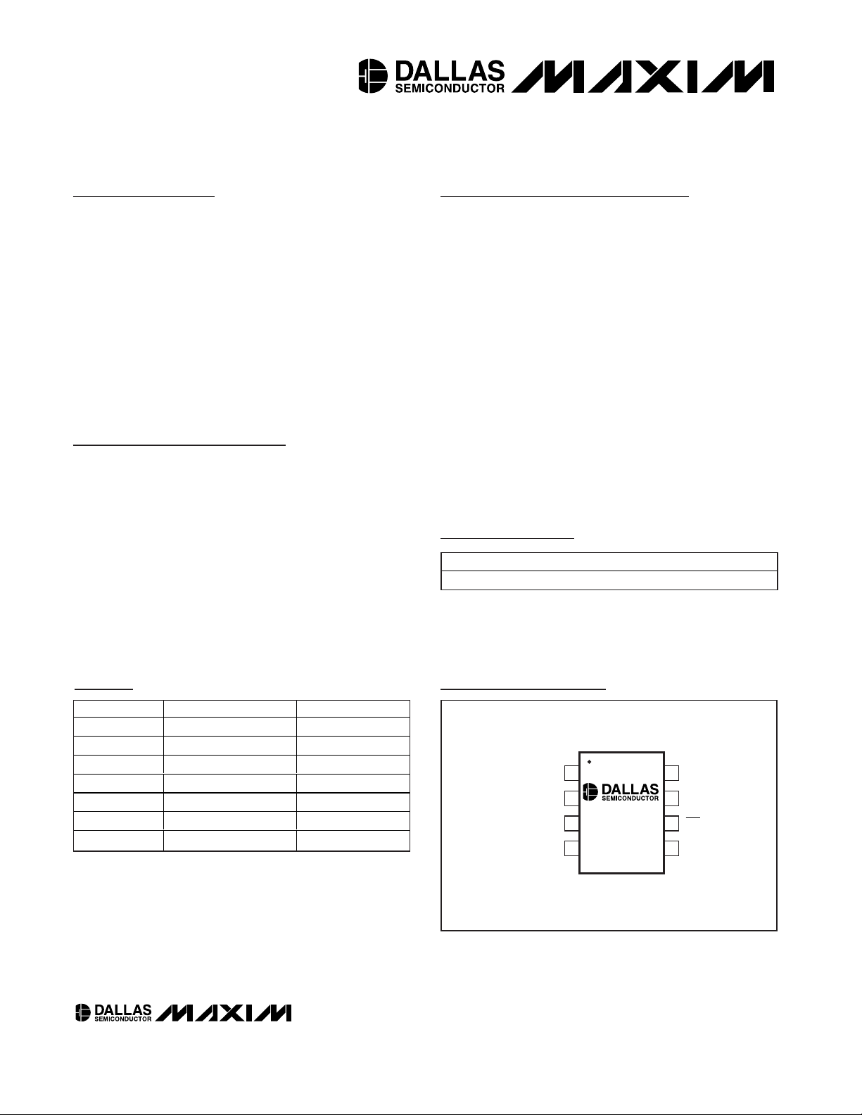
PDN
OEGND
1
2
87SCL
SDASPRD
V
CC
OUT
µSOP (118 mils)
TOP VIEW
3
4
6
5
DS1087L
Pin Configuration
Ordering Information
Rev 0; 7/03
For pricing, delivery, and ordering information, please contact Maxim/Dallas Direct! at
1-888-629-4642, or visit Maxim’s website at www.maxim-ic.com.
PART TEMP RANGE PIN-PACKAGE
DS1087LU-yxx -40°C to +85°C
8 µSOP (118 mils)
EconOscillator is a trademark of Dallas Semiconductor.
Typical Operating Circuits appear at end of data sheet.
Standard Frequency Options
PART
FREQUENCY (MHz)
SPREAD (%)
DS1087LU-202
2.0480 2
DS1087LU-402
2.0480 4
DS1087LU-210
10.0 2
DS1087LU-216
16.6 2
DS1087LU-266
66.6 2
DS1087LU-466
66.6 4
DS1087LU-yxx
Fixed up to 66.6 2 or 4
Custom frequencies and over 20 standard frequencies available, contact factory.
Page 2
DS1087L
3.3V Spread-Spectrum EconOscillator
2 _____________________________________________________________________
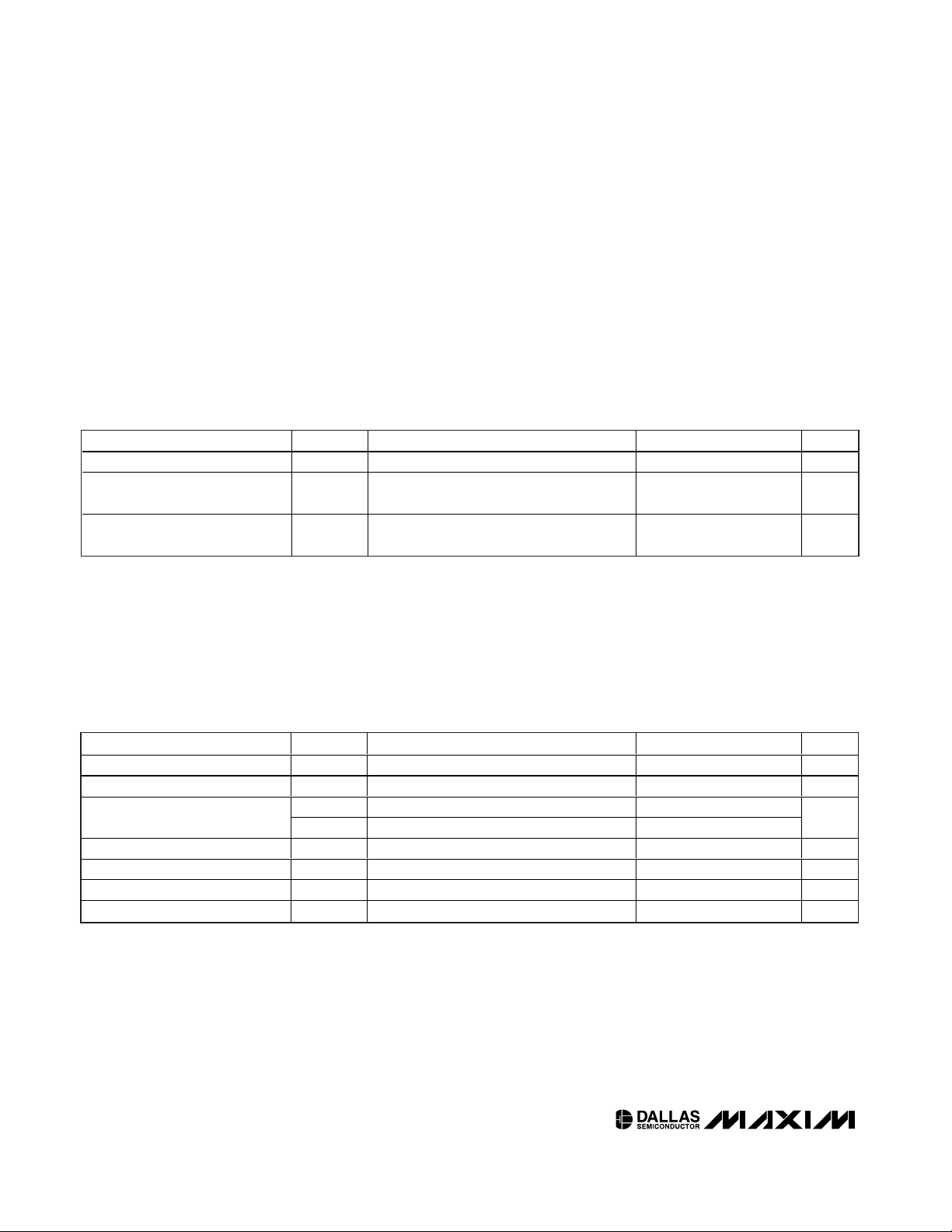
ABSOLUTE MAXIMUM RATINGS
RECOMMENDED DC OPERATING CONDITIONS
(VCC= 2.7V to 3.6V, TA= -40°C to +85°C.)
Stresses beyond those listed under “Absolute Maximum Ratings” may cause permanent damage to the device. These are stress ratings only, and functional
operation of the device at these or any other conditions beyond those indicated in the operational sections of the specifications is not implied. Exposure to
absolute maximum rating conditions for extended periods may affect device reliability.
PARAMETER
SYMBOL
CONDITION
MIN
TYP
MAX
UNITS
Supply Voltage V
CC
(Note 1) 2.7 3.6 V
High-Level Input Voltage
(SDA, SCL, SPRD, PDN, OE)
V
IH
0.7 x
V
CC
+
0.3
V
Low-Level Input Voltage
(SDA, SCL, SPRD, PDN, OE)
V
IL
0.3 x
V
DC ELECTRICAL CHARACTERISTICS
(VCC= 2.7V to 3.6V, TA= -40°C to +85°C.)
PARAMETER
CONDITION
UNITS
V
OH
IOH = -4mA, VCC = min 2.4 V
V
OL
IOL = 4mA 0.4 V
V
OL1
3mA sink current 0 0.4
V
OL2
6mA sink current 0 0.6
V
High-Level Input Current I
IH
VCC = 3.6V 1 µA
Low-Level Input Current I
IL
VIL = 0 -1 µA
Supply Current (Active) I
CC
CL = 15pF (output at f0)15mA
Standby Current (Power-Down) I
CCQ
Power-down mode 5 µA
Voltage Range on VCCRelative to Ground ..........-0.5V to +6.0V
Voltage Range on SPRD, PDN, OE, SDA, SCL
Relative to Ground* ................................-0.5V to (V
CC
+ 0.5V)
Operating Temperature Range ...........................-40°C to +85°C
Programming Temperature Range .........................0°C to +70°C
Storage Temperature Range .............................-55°C to +125°C
Soldering Temperature ..................See IPC/JEDEC J-STD-020A
*This voltage must not exceed 6.0V.
V
CC
High-Level Output Voltage (OUT)
Low-Level Output Voltage (OUT)
Low-Level Output Voltage (SDA)
SYMBOL
-0.3
MIN TYP MAX
V
CC
Page 3
DS1087L
3.3V Spread-Spectrum EconOscillator
_____________________________________________________________________ 3
MASTER OSCILLATOR CHARACTERISTICS
(VCC= 2.7V to 3.6V, TA= -40°C to +85°C.)
PARAMETER
CONDITION
UNITS
Master Oscillator Range
Available
f
0
MHz
Master Oscillator Frequency
Tolerance
∆
f
0
f
0
VCC = 3.3V, TA = +25°C (Note 2)
%
Voltage Frequency
Variation
∆
f
V
f
0
Over voltage range, TA = +25°C (Note 3)
%
Temperature Frequency Variation
∆
f
T
f
0
0°C to +70°C, VCC = 3.3V (Note 4)
%
Temperature Frequency Variation
∆
f
T
f
0
-40°C to +85°C, VCC = 3.3V (Note 4)
%
Prescaler bit J0 = 1 (Note 5) 2
Dither Frequency Range
Prescaler bit J0 = 0 (Note 5) 4
%
Dither Rate
Hz
AC ELECTRICAL CHARACTERISTICS
(VCC= 2.7V to 3.6V, TA= -40°C to +85°C.)
PARAMETER
SYMBOL
CONDITION
MIN
TYP
MAX
UNITS
Frequency Stable After
PRESCALER Change
1
period
Power-Up Time
t
POR
+
t
STAB
(Note 6) 0.1 0.5 ms
Enable of OUT After Exiting
Power-Down Mode
t
STAB
500 µs
OUT Disabled After Entering
Power-Down Mode
t
PDN
1ms
Load Capacitance C
L
(Note 7) 15 50 pF
Output Duty Cycle (OUT) TA = +25°C 45 55 %
SYMBOL
MIN TYP MAX
33.3 66.6
-0.5 +0.5
-0.75 +0.75
-0.5 +0.5
-1.5 +0.5
f0 / 2048
Page 4
DS1087L
3.3V Spread-Spectrum EconOscillator
4 _____________________________________________________________________
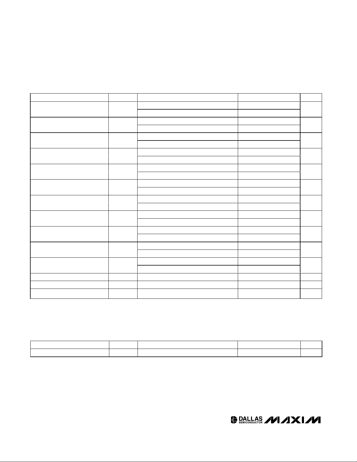
AC ELECTRICAL CHARACTERISTICS—2-WIRE INTERFACE
(VCC= 2.7V to 3.6V, TA= 0°C to +70°C.)
PARAMETER
SYMBOL
CONDITION
MIN
TYP
MAX
UNITS
Fast mode (Note 8) 400
SCL Clock Frequency f
SCL
Standard mode (Note 8) 100
kHz
Fast mode (Note 8)
Bus Free Time Between a STOP
and START Condition
t
BUF
Standard mode (Note 8) 4.7
µs
Fast mode (Notes 8 and 9) 0.6
Hold Time (repeated) START
Condition
Standard mode (Notes 8 and 9) 4.0
µs
Fast mode (Note 8) 1.3
LOW Period of SCL t
LOW
Standard mode (Note 8) 4.7
µs
Fast mode (Note 8) 0.6
HIGH Period of SCL t
HIGH
Standard mode (Note 8) 4.0
µs
Fast mode 0.6
Setup Time for a Repeated
START
t
SU:STA
Standard mode 4.7
µs
Fast mode (Notes 8, 10, and 11) 0 0.9
Data Hold Time
Standard mode (Notes 8, 10, and 11) 0 0.9
µs
Fast mode (Note 8)
Data Setup Time
Standard mode (Note 8)
ns
Fast mode (Note 12)
300
Rise Time of Both SDA and SCL
Signals
t
R
Standard mode (Note 12)
ns
Fast mode (Note 12)
300
Fall Time of Both SDA and SCL
Signals
t
F
Standard mode (Note 12)
ns
Fast mode 0.6
Setup Time for STOP
Standard mode 4.0
µs
Capacitive Load for Each Bus
C
B
(Note 12) 400 pF
NV Write Cycle Time t
WR
10 ms
Input Capacitance C
I
5pF
NONVOLATILE MEMORY CHARACTERISTICS
(VCC= 2.7V to 3.6V)
PARAMETER
SYMBOL
CONDITION
MIN
TYP
MAX
UNITS
Writes +70°C
1.3
t
HD:STA
t
HD:DAT
t
SU:DAT
t
SU:STO
100
250
20 + 0.1C
20 + 0.1C
20 + 0.1C
20 + 0.1C
10,000
B
B
B
B
1000
1000
Page 5

DS1087L
3.3V Spread-Spectrum EconOscillator
_____________________________________________________________________ 5
Note 1: All voltages are referenced to ground.
Note 2: This is the absolute accuracy of the master oscillator frequency at the default settings.
Note 3: This is the change that is observed in master oscillator frequency with changes in voltage from nominal voltage at
T
A
= +25°C.
Note 4: This is the percentage frequency change from the +25°C frequency due to temperature at V
CC
= 3.3V.
Note 5: The dither deviation of the master oscillator frequency is unidirectional and lower than the undithered frequency.
Note 6: This indicates the time elapsed between power-up and the output becoming active. An on-chip delay is intentionally
introduced to allow the oscillator to stabilize. t
stab
is equivalent to approximately 512 master clock cycles and depends
on the programmed master oscillator frequency.
Note 7: Output voltage swings may be impaired at high frequencies combined with high output loading.
Note 8: A fast-mode device can be used in a standard-mode system, but the requirement t
SU:DAT
> 250ns must then be met. This
is automatically the case if the device does not stretch the LOW period of the SCL signal. If such a device does stretch
the LOW period of the SCL signal, it must output the next data bit to the SDA line at least t
R MAX
+ t
SU:DAT
= 1000ns +
250ns = 1250ns before the SCL line is released.
Note 9: After this period, the first clock pulse is generated.
Note 10: A device must internally provide a hold time of at least 300ns for the SDA signal (referred to as the V
IH MIN
of the SCL sig-
nal) to bridge the undefined region of the falling edge of SCL.
Note 11: The maximum t
HD:DAT
need only be met if the device does not stretch the LOW period (t
LOW
) of the SCL signal.
Note 12: C
B
—total capacitance of one bus line, timing referenced to 0.9 x VCCand 0.1 x VCC.
Typical Operating Characteristics
(VCC= 3.3V, TA= +25°C, unless otherwise noted.)
ACTIVE SUPPLY CURRENT
vs. TEMPERATURE
DS1087L toc01
TEMPERATURE (°C)
CURRENT (mA)
80706050403020100-10-20-30
5.5
6.0
6.5
7.0
7.5
5.0
-40 90
VCC = 3.3V
FREQUENCY = 66.6MHz
OE = PDN = V
CC
15pF LOAD
8.2pF LOAD
4.7pF LOAD
UNLOADED
VOLTAGE (V)
3.5
3.42.8 2.9 3.0 3.23.1 3.3
1.0
2.0
3.0
4.0
5.0
6.0
7.0
8.0
0
2.7 3.6
ACTIVE SUPPLY CURRENT
vs. VOLTAGE
DS1087L toc02
CURRENT (mA)
FREQUENCY = 66.6MHz
OUTPUT UNLOADED
OE = PDN = V
CC
SUPPLY CURRENT vs. PRESCALER
DS1087L toc03
PRESCALER (DECIMAL)
10010
1 1000
1
2
3
4
5
6
7
0
CURRENT (mA)
OUTPUT UNLOADED
3.6V
3.3V
2.7V
Page 6

DS1087L
3.3V Spread-Spectrum EconOscillator
6 _____________________________________________________________________
FREQUENCY % CHANGE vs.
SUPPLY VOLTAGE
DS1087L toc07
VOLTAGE (V)
FREQUENCY % CHANGE (FROM 3.3V)
3.53.43.2 3.32.9 3.0 3.12.8
-0.80
-0.60
-0.40
-0.20
0
0.20
0.40
0.60
0.80
1.00
-1.00
2.7 3.6
OUTPUT LOADED WITH
12pF OSCILLOSCOPE PROBE
FREQUENCY = 66.6MHz
FREQUENCY % CHANGE vs.
TEMPERATURE
DS1087L toc08
TEMPERATURE (°C)
FREQUENCY % CHANGE (FROM 25°C)
80706050403020100-10-20-30
-1.00
-0.50
0
0.50
1.00
1.50
-1.50
-40 90
VCC = 3.3V
FREQUENCY = 66.6MHz
OUTPUT LOADED WITH
12pF OSCILLOSCOPE PROBE
ACTIVE SUPPLY CURRENT
vs. SCL FREQUENCY
SCL FREQUENCY (kHz)
SUPPLY CURRENT (mA)
300200100
1
2
3
4
5
6
7
0
0 400
DS1087L toc09
VCC = SDA = 3.3V
FREQUENCY = 66.6MHz
OUTPUT UNLOADED
DUTY CYCLE vs. VOLTAGE
DS1087L toc10
VOLTAGE (V)
DUTY CYCLE (%)
3.53.43.2 3.32.9 3.0 3.12.8
51
52
53
54
55
56
57
58
59
60
50
2.7 3.6
FREQUENCY = 66.6MHz
T
A
= +25°C
OUTPUT LOADED WITH
12pF OSCILLOSCOPE PROBE
TEMPERATURE (°C)
60
5030 402010070
DUTY CYCLE vs. TEMPERATURE
DS1087L toc11
DUTY CYCLE (%)
51
52
53
54
55
56
57
58
59
60
50
VCC = 3.3V
FREQUENCY = 66.6MHz
OUTPUT LOADED WITH
12pF OSCILLOSCOPE PROBE
Typical Operating Characteristics
(VCC= 3.3V, TA= +25°C, unless otherwise noted.)
1
2
3
4
5
6
0
SUPPLY CURRENT vs. PRESCALER
DS1087L toc04
PRESCALER (DECIMAL)
100101 1000
CURRENT (mA)
VCC = 3.3V
OUPUT UNLOADED
-40°C, +25°C, +85°C
0.5
1.0
1.5
2.0
2.5
3.0
3.5
4.0
0
SUPPLY CURRENT
vs. TEMPERATURE WITH OE = 0
DS1087L toc05
TEMPERATURE (°C)
CURRENT (mA)
80706050403020100-10-20-30-40 90
FREQUENCY = 66.6MHz
VCC = 2.7V
OUTPUT UNLOADED
FREQUENCY = 206.4kHz
SHUTDOWN SUPPLY CURRENT
vs. TEMPERATURE
DS1087L toc06
TEMPERATURE (°C)
CURRENT (µA)
807050 60-10 0 10 20 30 40-30 -20
0.2
0.4
0.6
0.8
1.0
1.2
1.4
1.6
1.8
2.0
0
-40 90
VCC = 3.3V
OUTPUT UNLOADED
Page 7

DS1087L
3.3V Spread-Spectrum EconOscillator
_____________________________________________________________________ 7
Pin Description
PIN NAME FUNCTION
1 OUT Oscillator Output
2 SPRD
Dither Enable. When the pin is high, the dither is enabled. When the pin is low, the dither is disabled.
3VCCPower Supply
4 GND Ground
5OE
Output Enable. When the pin is high, the output buffer is enabled. When the pin is low, the output is
disabled but the internal master oscillator is still on.
6 PDN
Power-Down. When the pin is high, the master oscillator is enabled. When the pin is low, the master
oscillator is disabled (power-down mode).
7 SDA 2-Wire Serial Data. This pin is for serial data transfer to and from the device.
8 SCL 2-Wire Serial Clock. This pin is used to clock data into and out of the device.
Figure 1. Functional Diagram
SDA
SCL
2-WIRE
INTERFACE
V
CC
EEPROM CONTROL
REGISTERS
PRESCALER
ADDR
SPRD
PDN
OUT
OE
TRIANGLE WAVE
GENERATOR
FACTORY-PROGRAMMED
OSCILLATOR
PRESCALER
BY 1, 2, 4...256
GND
MASTER
OSCILLATOR
OUTPUT
DITHER SIGNAL
DITHER
CONTROL
DS1087L
Page 8
DS1087L
3.3V Spread-Spectrum EconOscillator
8 _____________________________________________________________________
Detailed Description
A block diagram of the DS1087L is shown in Figure 1.
Output Frequency
The internal master oscillator can generate a square
wave with a frequency range of 33.3MHz to 66.6MHz.
The master oscillator frequency and output frequency
are factory programmed, although the user can use the
programmable divider to divide the master oscillator
frequency by 2x(where x equals 0 to 8).
Output Control and Power-Down
Two user control signals control the output. The outputenable pin, OE, gates the clock output buffer and the
PDN pin disables the master oscillator and turns off the
output for power-sensitive applications (note: the
power-down command must persist for at least two output frequency cycles plus 10µs for deglitching purpos-
es). On power-up, the output is disabled until power is
stable and the master oscillator has generated 512
clock cycles.
Both controls feature a synchronous enable, which
ensures there are no output glitches when the output is
enabled. The synchronous enable also ensures a constant time interval (for a given frequency setting) from
an enable signal to the first output transition.
Spread Spectrum
The DS1087L can reduce radiated emission peaks. The
output frequency can be dithered 2% or 4% below the
programmed frequency. Although the output frequency
changes when the dither is enabled, the duty cycle
does not change.
The dither is controlled by the J0 bit in the PRESCALER
register and enabled with the SPRD pin. The maximum
spectral attenuation occurs when the prescaler is set to
1. The spectral attenuation is reduced by 2.7dB for
every factor of 2 that is used in the prescaler. This happens because the prescaler’s divider function tends to
average the dither in creating the lower frequency.
However, the most stringent spectral emission limits are
imposed on the higher frequencies where the prescaler
is set to a low divider ratio.
A triangle-wave generator injects an offset element into
the master oscillator to dither its output. The dither rate
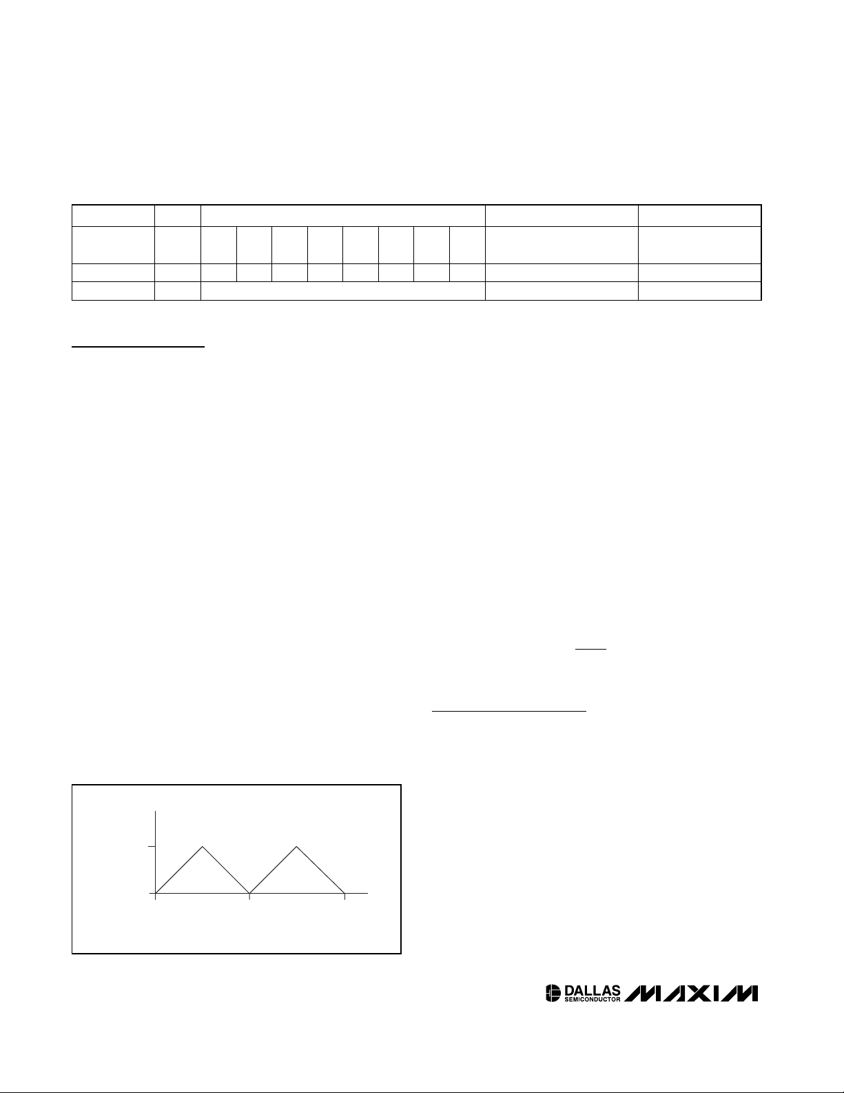
(see Equation 1) is based on the master oscillator frequency. Figure 2 shows a plot of the output frequency
versus dither rate.
where f0 = master oscillator frequency
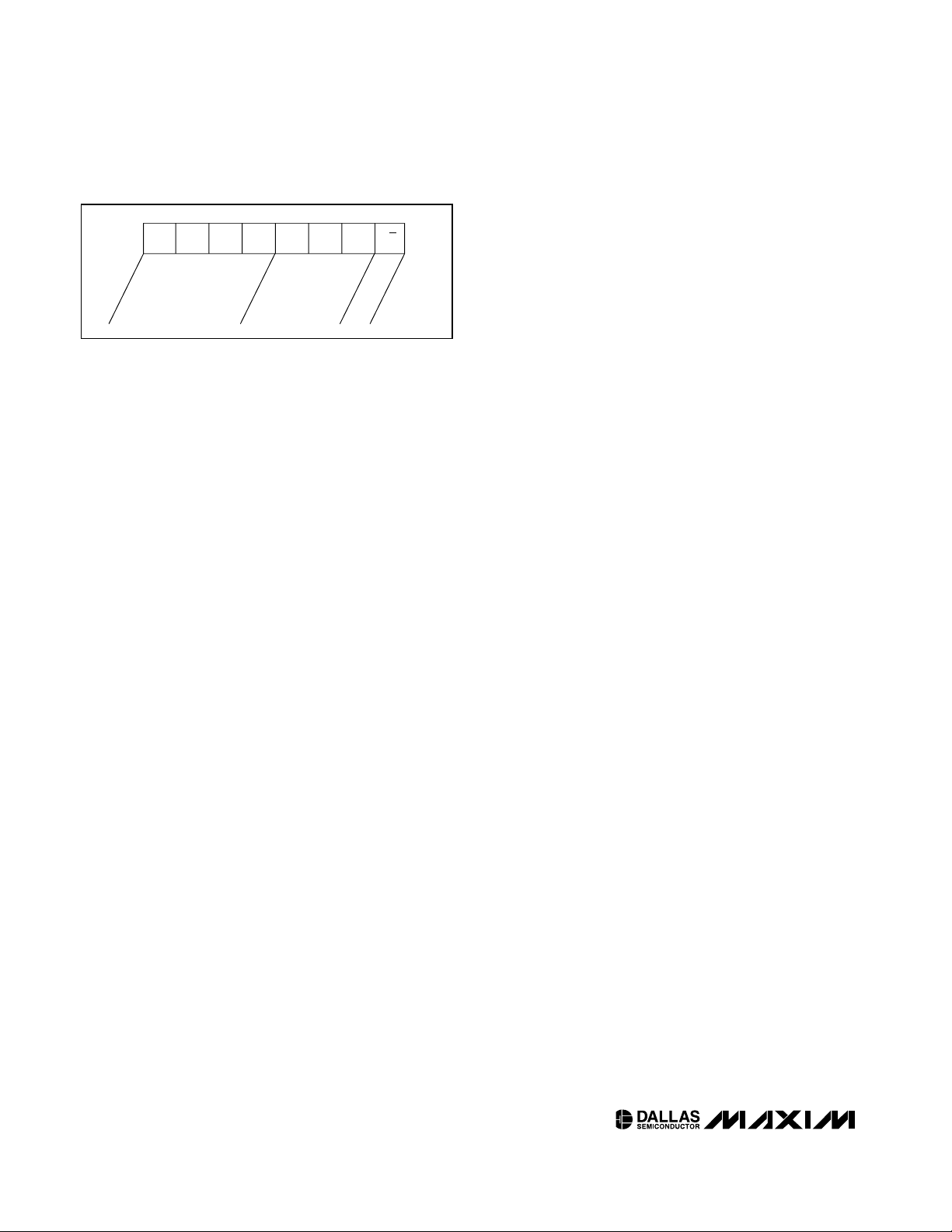
Register Summary
The DS1087L registers are used to change the dither
amount, output frequency, and slave address. A summary of the registers is shown in Table 1. Once programmed into EEPROM, the settings only need to be
reprogrammed if it is desired to reconfigure the device.
PRESCALER Register
Bit 5: Output Low or High-Z. The LO/HIZ bit
controls the output. During power-down,
while the output is deactivated, if the
LO/HIZ bit is set to 0, the output is high-Z.
If the LO/HIZ bit is set to 1, the output is
driven low.
Bit 4: Dither Control. The J0 bit controls the
dither applied to the output. When J0 is
high, 2% peak dither is selected. When
J0 is low, 4% peak dither is selected.
Dither Ratef =
0
2048
REGISTER
BINARY FACTORY DEFAULT ACCESS
PRESCALER
110- - - - - b R/W
ADDR
11110000b R/W
WRITE EE
No Data — —
Table 1. Register Summary
Figure 2. Output Frequency vs. Dither Rate
OUTPUT FREQUENCY
DITHER RATE
0
WHERE N = (2X)
f
0
= FACTORY PROGRAMMED MASTER OSCILLATOR FREQUENCY
2f
O
/2048fO/2048
f
O
/N
(f
O
/N) - 4%
(1)
X1= Don’t care; read as one.
ADDR
LO/
X
1
X
1
J0 P3 P2 P1 P0
HIZ
X
X1WC A2 A1 A0
1
02h X
0Dh X
3Fh
1
1
Page 9

DS1087L
3.3V Spread-Spectrum EconOscillator
_____________________________________________________________________ 9
Bits 3 to 0: Prescaler Divider. The prescaler bits
(bits P3 to P0) divide the master oscillator
frequency by 2xwhere x can be from 0 to
8. Any prescaler bit value entered that is
greater than 8 decodes as 8.
ADDR Register
Bit 3: Write Control. The WC bit determines if
the EEPROM is to be written to after register contents have been changed. If WC
= 0 (default), EEPROM is written automatically after a write. If WC = 1, the EEPROM is only written when the WRITE EE
command is issued. See the WRITE EE
Command section for more information.
Bits 2 to 0: Address. The A0, A1, A2 bits determine
the lower nibble of the 2-wire slave
address.
WRITE EE Command
The WRITE EE command is useful in closed-loop applications where the registers are frequently written. In
applications where the register contents are frequently
written, the WC bit should be set to 1 to prevent wearing out the EEPROM. Regardless of the value of the WC
bit, the value of the ADDR register is always written
immediately to EEPROM. When the WRITE EE command has been received, the contents of the registers
are copied into the EEPROM, thus locking in the register settings.
_______2-Wire Serial Port Operation
2-Wire Serial Data Bus
The DS1087L communicates through a 2-wire serial
interface. A device that sends data onto the bus is
defined as a transmitter, and a device receiving data
as a receiver. The device that controls the message is
called a "master." The devices that are controlled by the
master are "slaves." A master device that generates the
serial clock (SCL), controls the bus access, and generates the START and STOP conditions must control the
bus. The DS1087L operates as a slave on the 2-wire
bus. Connections to the bus are made through the
open-drain I/O lines SDA and SCL.
The following bus protocol has been defined (see
Figures 3 and 5):
• Data transfer can be initiated only when the bus is
not busy.
• During data transfer, the data line must remain
stable whenever the clock line is HIGH. Changes
in the data line while the clock line is HIGH are
interpreted as control signals.
Accordingly, the following bus conditions have been
defined:
Bus not busy: Both data and clock lines remain
HIGH.
Start data transfer: A change in the state of the
data line, from HIGH to LOW, while the clock is
HIGH, defines a START condition.
Stop data transfer: A change in the state of the
data line, from LOW to HIGH, while the clock line
is HIGH, defines the STOP condition.
STOP
CONDITION
OR REPEATED
START
CONDITION
REPEATED IF MORE BYTES
ARE TRANSFERRED
ACK
START
CONDITION
ACK
ACKNOWLEDGEMENT
SIGNAL FROM RECEIVER
ACKNOWLEDGEMENT
SIGNAL FROM RECEIVER
SLAVE ADDRESS
MSB
SCL
SDA
R/W
DIRECTION
BIT
12 678 9 12 893–7
Figure 3. 2-Wire Data Transfer Protocol
Page 10
DS1087L
3.3V Spread-Spectrum EconOscillator
10 ____________________________________________________________________
Data valid: The state of the data line represents
valid data when, after a START condition, the data
line is stable for the duration of the HIGH period of
the clock signal. The data on the line must be
changed during the LOW period of the clock signal. There is one clock pulse per bit of data.
Each data transfer is initiated with a START condition and terminated with a STOP condition. The
number of data bytes transferred between START
and STOP conditions is not limited, and is determined by the master device. The information is
transferred byte-wise and each receiver acknowledges with a ninth bit.
Within the bus specifications a standard mode
(100kHz clock rate) and a fast mode (400kHz
clock rate) are defined. The DS1087L works in
both modes.
Acknowledge: Each receiving device, when
addressed, is obliged to generate an acknowledge after the byte has been received. The master
device must generate an extra clock pulse that is
associated with this acknowledge bit.
A device that acknowledges must pull down the
SDA line during the acknowledge clock pulse in
such a way that the SDA line is stable LOW during
the HIGH period of the acknowledge-related clock
pulse. Of course, setup and hold times must be
taken into account. When the DS1087L EEPROM
is being written to, it is not able to perform additional responses. In this case, the slave DS1087L
sends a not acknowledge to any data transfer
request made by the master. It resumes normal
operation when the EEPROM operation is complete.
A master must signal an end of data to the slave
by not generating an acknowledge bit on the last
byte that has been clocked out of the slave. In this
case, the slave must leave the data line HIGH to
enable the master to generate the STOP condition.
Figures 3, 4, 5, and 6 detail how data transfer is
accomplished on the 2-wire bus. Depending upon
the state of the R/W bit, two types of data transfer
are possible:
1) Data transfer from a master transmitter to a slave
receiver. The first byte transmitted by the master is
the slave address. Next follows a number of data
bytes. The slave returns an acknowledge bit after
each received byte.
2) Data transfer from a slave transmitter to a master
receiver. The first byte (the slave address) is transmitted by the master. The slave then returns an
acknowledge bit. Next follows a number of data
bytes transmitted by the slave to the master. The
master returns an acknowledge bit after all
received bytes other than the last byte. At the end
of the last received byte, a not acknowledge is
returned.
The master device generates all the serial clock
pulses and the START and STOP conditions. A
transfer is ended with a STOP condition or with a
repeated START condition. Since a repeated
START condition is also the beginning of the next
serial transfer, the bus is not released.
The DS1087L can operate in the following two modes:
Slave receiver mode: Serial data and clock are
received through SDA and SCL. After each byte is
received, an acknowledge bit is transmitted.
START and STOP conditions are recognized as
the beginning and end of a serial transfer.
Address recognition is performed by hardware
after reception of the slave address and direction
bit.
Slave transmitter mode: The first byte is received
and handled as in the slave receiver mode.
However, in this mode, the direction bit indicates
that the transfer direction is reversed. Serial data
is transmitted on SDA by the DS1087L while the
serial clock is input on SCL. START and STOP
conditions are recognized as the beginning and
end of a serial transfer.
Slave Address
Figure 4 shows the first byte sent to the device. It
includes the device identifier, device address, and the
R/W bit. The device address must match the address
set in the ADDR register (bits A0, A1, and A2).
Registers/Commands
See Table 1 for the complete list of registers/commands and Figure 6 for an example of using them.
MSB
DEVICE
IDENTIFIER
DEVICE
ADDRESS
READ/WRITE BIT
1 011A2A1 A0 R/W
LSB
Figure 4. Slave Address
Page 11

DS1087L
3.3V Spread-Spectrum EconOscillator
____________________________________________________________________ 11
Application Information
Power-Supply Decoupling
To achieve the best results when using the DS1087L,
decouple the power supply with 0.01µF and 0.1µF
high-quality, ceramic, surface-mount capacitors.
Surface-mount components minimize lead inductance,
which improves performance, and ceramic capacitors
tend to have adequate high-frequency response for
decoupling applications. These capacitors should be
placed as close to the VCCand GND pins as possible.
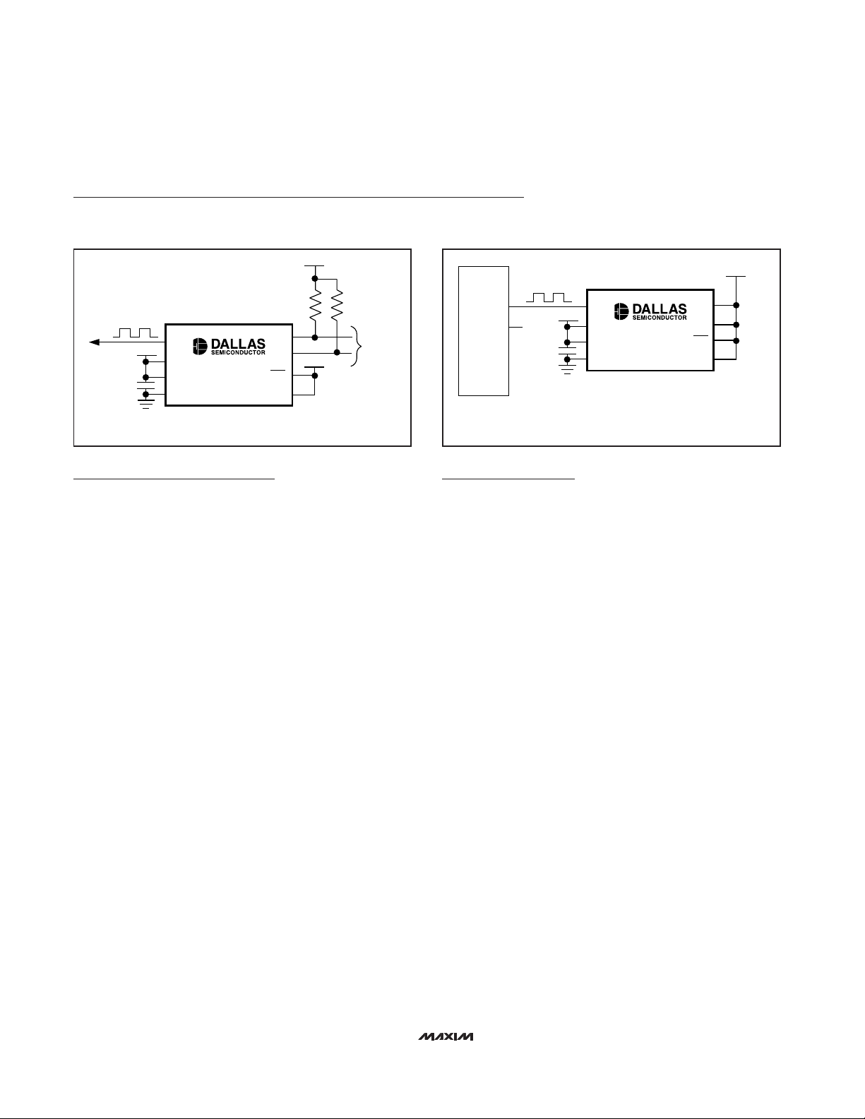
Stand-alone Mode
SCL and SDA cannot be left floating even in standalone mode. If the DS1087L never needs to be programmed in-circuit, including during production
testing, SDA and SCL can be wired high.
SDA
SCL
t
HD:STA
t
LOW
t
HIGH
t
R
t
F
t
BUF
t
HD:DAT
t
SU:DAT
REPEATED
START
t
SU:STA
t
HD:STA
t
SU:STO
t
SP
STOP START
Figure 5. 2-Wire AC Characteristics
SLAVE
ACK
10 1
1
R/WA0*A1*
SLAVE
ACK
A2*
MSB
LSB
DEVICE IDENTIFIER
DEVICE
ADDRESS
READ/
WRITE
MSB LSB
COMMAND/REGISTER ADDRESS
SLAVE
ACK
MSB LSB
b7 b6 b5 b4 b3 b2 b1 b0
SLAVE
ACK
STOP
*THE ADDRESS DETERMINED BY A0, A1, AND A2 MUST
MATCH THE ADDRESS SET IN THE ADDR REGISTER.
DATA
TYPICAL 2-WIRE WRITE TRANSACTION
EXAMPLE 2-WIRE TRANSACTIONS (WHEN A0, A1, AND A2 ARE ZERO)
A) SINGLE BYTE WRITE
-WRITE PRESCALER
REGISTER TO 128
B) SINGLE BYTE READ
-READ PRESCALER
REGISTER
START
START
START
B0h
B0h
SLAVE
ACK
SLAVE
ACK
02h
02h
SLAVE
ACK
SLAVE
ACK
DATA
SLAVE
ACK
STOP
10110000
10110000
b7 b6 b5 b4 b3 b2 b1 b0
00000010 10000000
10000000
00000010
REPEATED
START
DATA
MASTER
NACK
STOP
SLAVE
ACK
10110001
B1h
Figure 6. 2-Wire Transactions
Page 12
DS1087L
3.3V Spread-Spectrum EconOscillator
Maxim cannot assume responsibility for use of any circuitry other than circuitry entirely embodied in a Maxim product. No circuit patent licenses are
implied. Maxim reserves the right to change the circuitry and specifications without notice at any time.
12 ____________________Maxim Integrated Products, 120 San Gabriel Drive, Sunnyvale, CA 94086 408-737-7600
© 2003 Maxim Integrated Products Printed USA is a registered trademark of Maxim Integrated Products.
Chip Topology
TRANSISTOR COUNT: 10000
SUBSTRATE CONNECTED TO GROUND
Typical Operating Circuits
Package Information
For the latest package outline information, go to
www.maxim-ic.com/DallasPackInfo
DS1087L
DITHERED 130kHz TO
66.6MHz OUTPUT
DECOUPLING CAPACITORS
(0.1µF and 0.01µF)
SPRD
OUT
V
CC
V
CC
V
CC
4.7kΩ 4.7kΩ
V
CC
2-WIRE
INTERFACE
GND
SCL
SDA
PDN
OE
Processor-Controlled Mode
DS1087L
XTL1/OSC1
MICRO-
PROCESSOR
XTL2/OSC2
DITHERED 130kHz TO
66.6MHz OUTPUT
DECOUPLING CAPACITORS
(0.1µF and 0.01µF)
*SDA AND SCL CAN BE CONNECTED DIRECTLY HIGH IF THE DS1087L NEVER NEEDS
TO BE PROGRAMMED IN-CIRCUIT, INCLUDING DURING PRODUCTION TESTING.
SPRD
OUT
V
CC
V
CC
V
CC
GND
N.C.
SCL*
SDA*
PDN
OE
Stand-Alone Mode
 Loading...