

Page 1
General Description
The DS1081L is a spread-spectrum clock modulator IC
that reduces EMI in high clock-frequency-based, digital
electronic equipment.
Using an integrated phase-locked loop (PLL), the
DS1081L accepts an input clock signal in the range of
20MHz to 134MHz and delivers a spread-spectrum modulated output clock signal. The PLL modulates, or dithers,
the output clock about the center input frequency at a
pin-selectable magnitude and dither rate, allowing direct
EMI control and optimization. In addition, through an
enable pin the dithering can be enabled or disabled for
easy comparison of system performance during EMI testing. This same input pin also allows the DS1081L output
to be tri-stated.
By dithering the system clock, all the address, data,
and timing signals generated from this signal are also
dithered so that the measured EMI at the fundamental
and harmonic frequencies is greatly reduced. This is
accomplished without changing clock rise/fall times or
adding the space, weight, design time, and cost associated with mechanical shielding.
The DS1081L is provided in an 8-pin TSSOP package
and operates over a full automotive temperature range
of -40°C to +125°C.
Applications
LCD Panels for TVs, Desktop Monitors, and
Notebook and Tablet PCs
Automotive Telematics and Infotainment
Printers
Features
♦ Modulates a 20MHz to 134MHz Clock with Center
Spread-Spectrum Dithering
♦ Selectable Spread-Spectrum Modulation
Magnitudes of:
±0.5%
±1.0%
±1.5%
±2.0%
♦ Low 75ps Cycle-to-Cycle Jitter
♦ Spread-Spectrum Disable Mode
♦ Pin Compatible with Alliance/PulseCore
Semiconductor P2040 Series Devices
♦ Clock Output Disable
♦ Low Cost
♦ Low Power Consumption
♦ 3.3V Single Voltage Supply
♦ -40°C to +125°C Temperature Range
♦ Small 8-Pin TSSOP Package
DS1081L
20MHz to 134MHz Spread-Spectrum
Clock Modulator for LCD Panels
______________________________________________
Maxim Integrated Products
1
Rev 0; 4/07
For pricing, delivery, and ordering information, please contact Maxim/Dallas Direct! at
1-888-629-4642, or visit Maxim’s website at www.maxim-ic.com.
+
Denotes lead-free package.
T
Denotes tape-and-reel.
Ordering Information
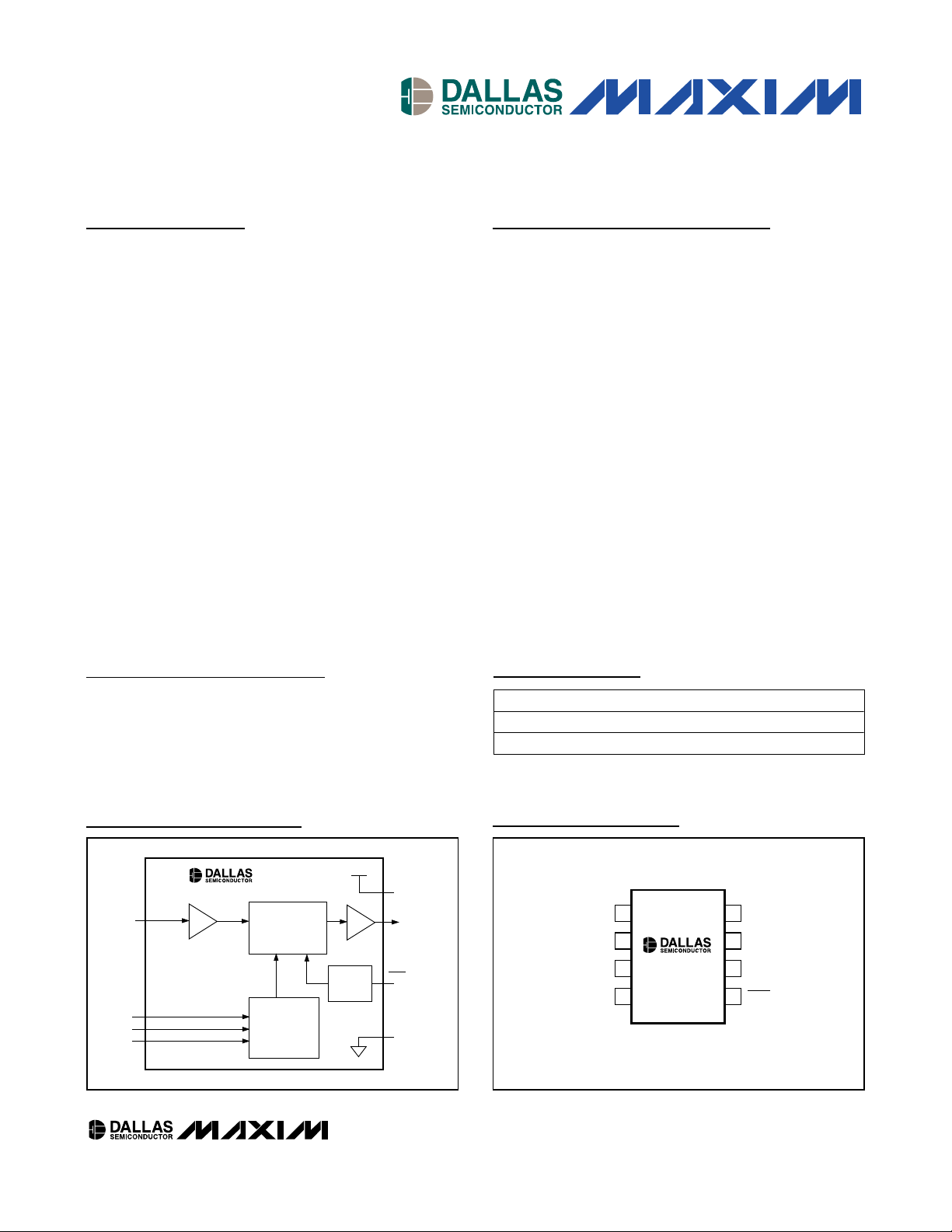
Block Diagram
Pin Configuration and Typical Operating Circuit appear at
end of data sheet.
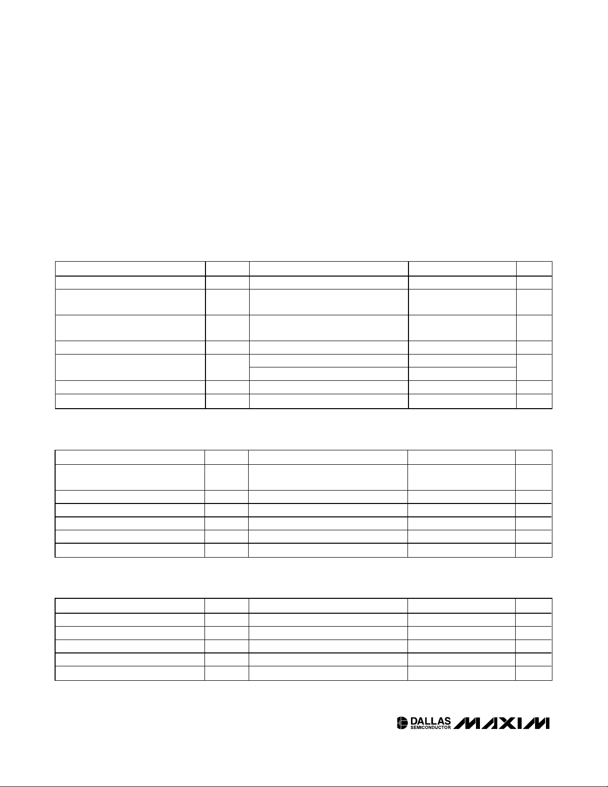
SSO
GND
1
2
8
7 CRSELSMSEL1
SMSEL2
CLKIN
TSSOP
(4.40mm)
TOP VIEW
3
4
6
5
DS1081L
V
CC
SSEN
Pin Configuration
PART TEMP RANGE PIN-PACKAGE
DS1081LE+ -40°C to +125°C 8 TSSOP
DS1081LE+T -40°C to +125°C 8 TSSOP
V
CC
DS1081L
CLKIN
fIN = 20MHz TO
134MHz
CRSEL
SMSEL1
SMSEL2
PLL WITH CENTER-
CONFIGURATION
DITHERED
SPREAD
SPECTRUM
DECODE AND
CONTROL
ENABLE
LOGIC
V
CC
SSO
= 20MHz to
f
SSO
134MHz (DITHERED)
SSEN
GND
Page 2
ABSOLUTE MAXIMUM RATINGS
RECOMMENDED OPERATING CONDITIONS
(TA= -40°C to +125°C, unless otherwise noted.)
Stresses beyond those listed under “Absolute Maximum Ratings” may cause permanent damage to the device. These are stress ratings only, and functional
operation of the device at these or any other conditions beyond those indicated in the operational sections of the specifications is not implied. Exposure to
absolute maximum rating conditions for extended periods may affect device reliability.
Voltage Range on VCCRelative to GND .............-0.5V to +3.63V
Voltage Range on Any Lead Relative
to GND ................-0.5V to (V
CC
+ 0.5V), not to exceed +3.63V
Operating Temperature Range .........................-40°C to +125°C
Storage Temperature Range .............................-55°C to +125°C
Soldering Temperature...................See J-STD-020 Specification
DC ELECTRICAL CHARACTERISTICS
(VCC= +3.0V to +3.6V, TA= -40°C to +125°C, unless otherwise noted.)
AC ELECTRICAL CHARACTERISTICS
(VCC= +3.0V to +3.6V, TA= -40°C to +125°C, unless otherwise noted.)
DS1081L
20MHz to 134MHz Spread-Spectrum
Clock Modulator for LCD Panels
2 _____________________________________________________________________
Note 1: All voltages referenced to ground. Currents into the IC are positive and out of the IC are negative.
Note 2: Time between power applied to device and stable output.
Supply Voltage VCC (Note 1) 3.0 3.6 V
Input Logic 1 V
Input Logic 0 VIL -0.3
Input Logic Float (SSEN, CRSEL) V
SSO Load C
CLKIN Frequency fIN 20 134 MHz
CLKIN Duty Cycle f
PARAMETER SYMBOL CONDITIONS MIN TYP MAX UNITS
IH
0V < VIN < VCC ±1 μA
FLOAT
SSO < 80MHz 15
L
80MHz SSO < 134MHz 7
40 60 %
INDC
0.8 x
V
CC
VCC +
0.3
0.2 x
V
CC
V
V
pF
Supply Current I
SMSEL1/SMSEL2/CLKIN Input Leakage I
CRSEL/SSEN Input Leakage I
Output Leakage (SSO) I
Low-Leve l Output Voltage (SSO) VOL IOL = 4mA 0.4 V
High-Level Output Voltage (SSO) VOH IOH = -4mA 2.4 V
PARAMETER SYMBOL CONDITIONS MIN TYP MAX UNITS
CL = 7pF
CC
IL:1
IL:2
OZ
= 134MHz
f
IN
0V < VIN < VCC -1 +1 μA
0V < VIN < VCC -100 +100 μA
SSEN = float -1 +1 μA
15 mA
SSO Duty Cycle f
SSO Ri se Time tR CL = 7pF 1 ns
SSO Fal l Time tF CL = 7pF 1 ns
Peak Cycle-to-Cycle Jitter tJ TA = -40°C to +85°C, 10,000 cyc les 75 ps
Power-Up Time t
PARAMETER SYMBOL CONDITIONS MIN TYP MAX UNITS
Measured at VCC/2 40 60 %
SSODC
(Note 2) 50 ms
POR
Page 3

DS1081L
20MHz to 134MHz Spread-Spectrum
Clock Modulator for LCD Panels
_____________________________________________________________________
3
Typical Operating Characteristics
(TA = +25°C, unless otherwise noted.)
SUPPLY CURRENT vs. SUPPLY VOLTAGE
DS1081L toc01
SUPPLY VOLTAGE (V)
SUPPLY CURRENT (mA)
3.53.43.33.23.1
2
4
6
8
10
12
14
0
3.0 3.6
CLKIN = 134MHz
CLKIN = 20MHz
CLKIN = 66MHz
SUPPLY CURRENT vs. TEMPERATURE
DS1081L toc02
TEMPERATURE (°C)
SUPPLY CURRENT (mA)
12010080604020-20 0
2
4
6
8
10
12
14
0
-40
CLKIN = 134MHz
CLKIN = 33MHz
CLKIN = 66MHz
134
SUPPLY CURRENT vs. FREQUENCY
DS1081L toc03
FREQUENCY (MHz)
SUPPLY CURRENT (mA)
11696765636
2
4
6
8
10
12
14
0
20
VCC = 3.6V
VCC = 3.0V
DUTY CYCLE vs. TEMPERATURE
DS1081L toc04
TEMPERATURE (°C)
DUTY CYCLE (%)
12010060 800 20 40-20
42
44
46
48
50
52
54
56
58
60
40
-40
CLKIN = 66MHz
DUTY CYCLE vs. SUPPLY VOLTAGE
DS1081L toc05
SUPPLY VOLTAGE (V)
DUTY CYCLE (%)
3.53.43.33.23.1
42
44
46
48
50
52
54
56
58
60
40
3.0 3.6
CLKIN = 66MHz
SPECTRUM ATTENUATION vs. FREQUENCY
AT DIFFERENT DITHER AMPLITUDES
DS1081L toc06
FREQUENCY (MHz)
ATTENUATION (dB)
f
OUT
= 40MHz
±
2%
±
1.5%
0.5%
6dB
4.5dB
3dB
±
1%
f
OUT
= 40MHz
RBW = 120KHz
CENTER DITHER
Page 4

Detailed Description
The DS1081L modulates an input clock to generate a
center-dithered spread-spectrum output. A 20MHz to
134MHz clock is applied to the CLKIN pin. An internal
PLL dithers the output clock about its center frequency
at a user-selectable magnitude.
Spread-Spectrum Dither Magnitude
The DS1081L can generate dither magnitudes up to
±2%. The desired magnitude is selected using input pins
SMSEL1 and SMSEL2 as shown in Table 1.
Spread-Spectrum Dither Rate
The output spread-spectrum dither rate is determined
by the input frequency to maximize EMI reduction and
to ensure that the dither rate is always above the audio
frequency range. The user must configure CRSEL,
based on Table 2, depending on the input frequency
(fIN) so that the appropriate dither rate is programmed.
DS1081L
20MHz to 134MHz Spread-Spectrum
Clock Modulator for LCD Panels
4 _____________________________________________________________________
Pin Description
PIN NAME FUNCTION
1
CLKIN
Clock Input. 20MHz to 134MHz clock input (fIN).
Spread-Spectrum Magnitude Select Inputs. The se digital inputs select the desired spread-spectrum
magnitude as shown in the table below.
SMSEL2 SMSEL1 MAGNITUDE SELECTED
2 SMSEL2
0 0 ±2.0%
0 1 ±1.5%
1 0
±1.0%
3SMSEL1
1 1 ±0.5%
4
GND Ground
5 SSEN
Spread-Spectrum Enable. Three-level input to enable/di sable spread-spectrum and to tri-state the output.
0 = Power-up/spread-spectrum enabled.
Float = SSO tri-stated.
1 = Power-up/spread-spectrum disabled (not a bypas s mode).
6 SSO
Spread-Spectrum Clock Output. Outputs a center-dithered spread-spectrum version of the clock input at
CLKIN.
Cloc k Range and Dither Rate Select. Three-level input that determines the dither rate. See the Detailed
Description section for details.
CRSEL CLKIN RANGE DITHER RATE
0 66MHz to 134MHz fIN/2048
Float 33MHz to 80MHz fIN/1024
7 CRSEL
1 20MHz to 38MHz f
IN
/512
8
V
CC
Supply Voltage
Table 2.
Table 1.
SMSEL2
00±2.0%
01±1.5%
10±1.0%
11±0.5%
SMSEL1 MAGNITUDE
CRSEL CLKIN RANGE DITHER RATE
0 66MHz to 134MHz fIN/2048
Float 33MHz to 80MHz fIN/1024
1 20MHz to 38MHz fIN/512
Page 5

DS1081L
20MHz to 134MHz Spread-Spectrum
Clock Modulator for LCD Panels
Maxim cannot assume responsibility for use of any circuitry other than circuitry entirely embodied in a Maxim product. No circuit patent licenses are
implied. Maxim reserves the right to change the circuitry and specifications without notice at any time.
Maxim Integrated Products, 120 San Gabriel Drive, Sunnyvale, CA 94086 408-737-7600 _____________________
5
© 2007 Maxim Integrated Products is a registered trademark of Maxim Integrated Products, Inc.
is a registered trademark of Dallas Semiconductor Corporation.
Spread-Spectrum Enable
On power-up, the output clock (SSO) remains tri-stated
until the internal PLL reaches a stable frequency. The
SSEN input can be used to disable the spread-spectrum modulation and to tri-state the SSO output. If the
SSEN pin is pulled high, the spread-spectrum modulation is turned off, but the device still uses the internal
PLL to generate the clock signal at SSO. If the SSEN pin
is floated, the output will be tri-stated.
Application Information
Power-Supply Decoupling
To achieve best results, it is highly recommended that a
decoupling capacitor is used on the IC power-supply
pins. Typical values of decoupling capacitors are 0.01µF
and 0.1µF. Use a high-quality, ceramic, surface-mount
capacitor, and mount it as close as possible to the V
CC
and GND pins of the IC to minimize lead inductance.
Figure 1. DS1081L Spread-Spectrum Frequency Modulation
CLKIN
SMSEL1
SMSEL2
GND
CRSEL
V
CC
DECOUPLING
CAPACITOR
V
CC
SSO
fIN = 20MHz TO
134MHz
NOTE: IN THE ABOVE CONFIGURATION WITH SMSEL1, SMSEL2, AND SSEN CONNECTED TO GND AS WELL AS
CRSEL CONNECTED TO V
CC
AND SSEN CONNECTED TO GND, THE DEVICE IS CONFIGURED WITH A
SPREAD-SPECTRUM MAGNITUDE OF ±2.0%, AND ALLOWS A CLKIN BETWEEN 20MHz and 38MHz.
DS1081L
f
SSO
DITHERED
SSEN
Typical Operating Circuit
Package Information
For the latest package outline information, go to www.maxim-ic.com/DallasPackInfo.
fIN + (0.5%, 1.0%, 1.5%, OR 2.0% OF fIN)
f
IN
fIN - (0.5%, 1.0%, 1.5%, OR 2.0% OF fIN)
f
SSO
CLKIN RANGE (MHz) DITHER RATE
66 TO 134 f
33 TO 80 f
20 TO 38 f
IN
IN
IN
/2048
/1024
/512
1
DITHER CYCLE
RATE
IF SSEN = 1
DITHER AMOUNT
(±0.5%, ±1.0%, ±1.5%, OR ±2.0%)
TIME
 Loading...