

Page 1
April 2002
CLC5957
12-Bit, 70 MSPS Broadband Monolithic A/D Converter
CLC5957 12-Bit, 70 MSPS Broadband Monolithic A/D Converter
General Description
The CLC5957 is a monolithic 12-bit, 70MSPS analog-todigital converter. The device has been optimized for use in
IF-sampled digital receivers and other applications where
high resolution, high sampling rate, wide dynamic range, low
power dissipation, and compact size are required. The
CLC5957 features differential analog inputs, low jitter differential universal clock inputs, a low distortion track-and-hold
with 0-300MHz input bandwidth, a bandgap voltage reference, data valid clock output, TTL compatible CMOS (3.3V
or 2.5V) programmable output logic, and a proprietary 12-bit
multi-stage quantizer. The CLC5957 is fabricated on the
ABIC-V 0.8 micron BiCMOS process.
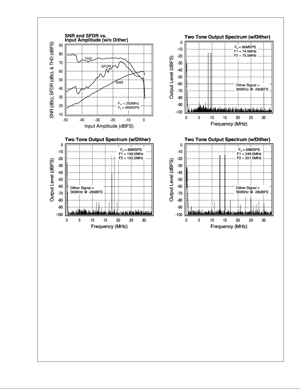
The CLC5957 features a 74dBc spurious free dynamic
range (SFDR) and a 67dB signal to noise ratio (SNR). The
wideband track-and-hold allows sampling of IF signals to
greater than 250MHz. The part produces two-tone, dithered,
SFDR of 83dBFS at 75MHz input frequency. The differential
analog input provides excellent common mode rejection,
while the differential universal clock inputs minimize jitter.
The 48-pin TSSOP package provides an extremely small
footprint for applications where space is a critical consideration. The CLC5957 operates from a single +5V power
supply. Operation over the industrial temperature range of
-40˚C to +85˚C is guaranteed. National Semiconductor tests
each part to verify compliance with the guaranteed specifications.
Features
n 70MSPS
n Wide dynamic range:
— SFDR: 74dBc
— SFDR with dither: 85dBFS
— SNR: 67dB
n IF sampling capability
n Input bandwidth = 0-300MHz
n Low power dissipation: 640mW
n Very small package: 48-pin TSSOP
n Single +5V supply
n Data valid clock output
n Programmable output levels: 3.3V or 2.5V
Applications
n Cellular base stations
n Digital communications
n Infrared/CCD imaging
n IF sampling
n Electro-optics
n Instrumentation
n Medical imaging
n High definition video
01502928
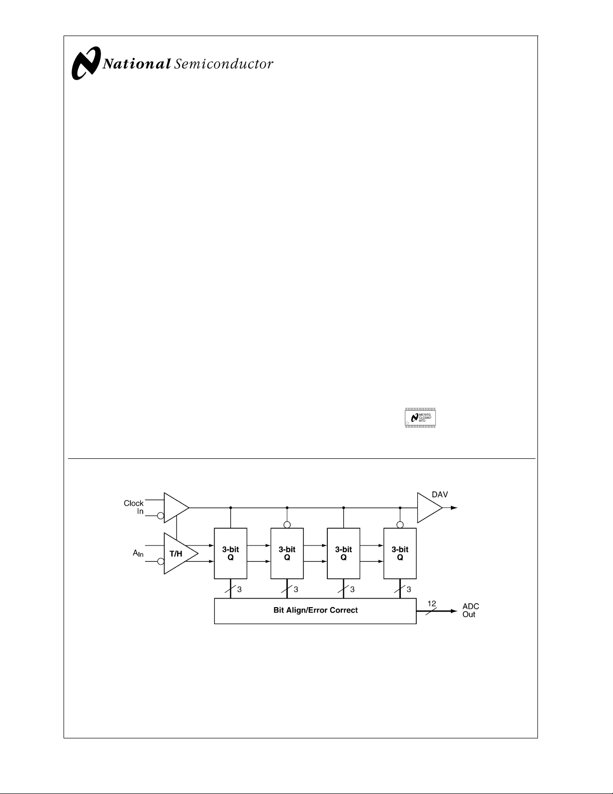
Block Diagram
01502902
© 2002 National Semiconductor Corporation DS015029 www.national.com
Page 2
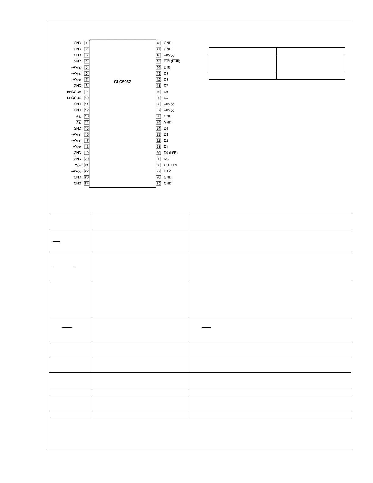
Pin Configuration
CLC5957
01502901
Ordering Information
CLC5957MTD 48-Pin TSSOP
CLC5957MTDX 48-Pin TSSOP (Taped
Reel)
CLC5957PCASM Evaluation Board
Pin Descriptions
Pin
Name
A
IN
A
IN
ENCODE
ENCODE
V
CM
D0–D11
GND
+AV
+DV
CC
CC
1–4, 8, 11, 12, 15, 19,
20, 23–26, 35, 36, 47, 48
NC 29 No connect. May be left open or grounded.
DAV 27
OUTLEV 28 Output Logic 3.3V or 2.5V option. Open = 3.3V, GND = 2.5V.
Pin
No.
13, 14
9, 10
21
30–34,
39–45
5–7, 16–18, 22
37, 38, 46
Description
Differential input with a common mode voltage of +2.4V. The ADC
full scale input is 1.024 VPPon each of the complimentary input
signals.
Differential clock where ENCODE initiates a new data conversion
cycle on each rising edge. Logic for these inputs are a 50% duty
>
cycle universal differential signal (
internally biased to V
/2 with a termination impedance of 2.5kΩ.
CC
200mV). The clock input is
Internal common mode voltage reference. Nominally +2.4V. Can be
used for the input common mode voltage. This voltage is derived
from an internal bandgap reference. V
should be buffered when
CM
driving any external load. Failure to buffer this signal can cause
errors in the internal bias currents.
Digital data outputs are CMOS and TTL compatible. D0 is the LSB
and D11 is the MSB. MSB is inverted. Output coding is two’s
complement. Current limited to source/sink 2.5mA typical.
Circuit ground.
+5V power supply for the analog section. Bypass to ground with a
0.1 µF capacitor.
+5V power supply for the digital section. Bypass to ground with a
0.1 µF capacitor.
Data Valid Clock. Data is valid on rising edge. Current limited to
source/sink 5mA typical.
www.national.com 2
Page 3
CLC5957
Absolute Maximum Ratings (Note 1)
If Military/Aerospace specified devices are required,
Recommended Operating Conditions
please contact the NationalSemiconductorSales Office/
Distributors for availability and specifications.
Positive Supply Voltage (V
) −0.5V to +6V
CC
Differential Voltage between any two
<
100 mV
Positive Supply Voltage (VCC) +5V±5%
Analog Input Voltage Range 2.048 V
PP
Operating Temperature Range −40˚C to +85˚C
Grounds
Analog Input Voltage Range GND to V
Digital Input Voltage Range −0.5V to +V
Output Short Circuit Duration
CC
CC
Package Thermal Resistance (Note 7)
Package θ
JA
48-Pin TSSOP 56˚C/W 16˚C/W
θ
JC
(one-pin to ground) Infinite
Junction Temperature (Note 7) 175˚C
Storage Temperature Range −65˚C to +150˚C
Lead Solder Duration (+300˚C) 10 sec.
Reliability Information
Transistor Count 5000
ESD tolerance
human body model
machine model
2000V
200V
Converter Electrical Characteristics
The following specifications apply for AVCC=DVCC= +5V, 66MSPS. Boldface limits apply for TA=T
+85˚C, all other limits T
= 25˚C (Note 3).
A
Symbol Parameter Conditions Min Typ Max Units
DYNAMIC PERFORMANCE
BW Large-Signal Bandwidth A
Overvoltage Recovery Time A
t
A
t
AJ
Effective Aperture Delay −0.41 ns
Aperture Jitter 0.3 ps(rms)
= −3 dBFS 300 MHz
IN
= 1.5 FS (0.01%) 12 ns
IN
NOISE AND DISTORTION
= 5 MHz, AIN= −1dBFS 67 dBFS
f
IN
SNR
*
(Note 2)
SFDR
IMD
Signal-to-Noise Ratio (without 50
harmonics)
Spurious-Free Dynamic Range
Spurious-Free Dynamic Range
(dithered)
Intermodulation Distortion
Intermodulation Distortion (dithered)
f
= 25 MHz, AIN= −1dBFS
IN
f
= 75 MHz, AIN= −3dBFS 65 dBFS
IN
f
= 150 MHz, AIN= −15dBFS 66 dBFS
IN
f
= 250 MHz, AIN= −15dBFS 66 dBFS
IN
f
= 5 MHz, AIN= −1dBFS 74 dBc
IN
f
= 25 MHz, AIN= −1dBFS
IN
f
= 75 MHz, AIN= −3dBFS 72 dBc
IN
f
= 150 MHz, AIN= −15dBFS 69 dBc
IN
f
= 250 MHz, AIN= −15dBFS 65 dBc
IN
= 19 MHz, AIN= −6dBFS 85 dBFS
f
IN
= 149.84 MHz, f
f
IN1
MHz, A
f
IN1
MHz, A
f
IN1
A
IN
= −10dBFS
IN
= 249.86 MHz, f
= −10dBFS
IN
= 74 MHz, f
= −12dBFS
IN2
IN2
= 75 MHz,
IN2
*
*
= 149.7
= 249.69
60 66 dBFS
60 74 dBc
68 dBFS
58 dBFS
83 dBFS
DC ACCURACY AND PERFORMANCE
DNL Differential Non-Linearity f
INL Integral Non-Linearity f
= 5MHz, AIN= −1dBFS
IN
= 5MHz, AIN= −1dBFS
IN
±
0.65 LSB
±
1.5 LSB
Offset Error (Note 2) −30 0 30 mV
Gain Error 1.2 % FS
V
REF
Reference Voltage (Note 2) 2.2 2.37 2.6 V
No Missing Codes (Note 2) f
= 5MHz, AIN= -1dBFS Guaranteed
IN
= −40˚C to T
min
max
diff.
=
www.national.com3
Page 4
Converter Electrical Characteristics (Continued)
The following specifications apply for AVCC=DVCC= +5V, 66MSPS. Boldface limits apply for TA=T
+85˚C, all other limits T
CLC5957
= 25˚C (Note 3).
A
Symbol Parameter Conditions Min Typ Max Units
ANALOG INPUTS
V
IN
RIN(SE)
R
IN
C
IN
Analog Diff Input Voltage Range 2.048 V
Analog Input Resistance
(Single-Ended)
500 Ω
(Diff) Analog Input Resistance (Differential) 1000 Ω
Analog Input Capacitance
(Single-ended)
2pF
ENCODE INPUTS (UNIVERSAL)
V
IH
V
IL
Logic Input High Voltage (Note
4),(Note 5)
Logic Input Low Voltage(Note
4),(Note 5)
Differential Input Swing (Note
4),(Note 5)
0V
0.2 V
DIGITAL OUTPUTS
V
OL
V
OH
Logic Output Low Voltage (Note 2) 0.01 0.4 V
Logic Output High Voltage (Note 2)
OUTLEV = 1 (open) 3.2 3.5 3.8 V
OUTLEV = 0 (GND) 2.4 2.7 3.0 V
TIMING (Note 6)
t
t
t
t
t
t
t
P
M
DNV
DGV
DAV
S
H
Maximum Conversion Rate
(ENCODE) (Note 2)
Minimum Conversion Rate
(ENCODE)
Pulse Width High (ENCODE) (Note
4)
50% threshold 7.1 ns
Pulse Width Low (ENCODE) (Note 4) 50% threshold 7.1 ns
ENCODE falling edge to DATA not
valid (Note 4)
ENCODE falling edge to DATA
guaranteed valid (Note 4)
Rising ENCODE to rising DAV delay
(Note 4)
50% threshold 8.3 12.6 ns
DATA setup time before rising DAV
(Note 4)
DATA hold time after rising DAV
(Note 4)
70 75 MSPS
10 MSPS
8.3 ns
−2.4 ns
t
M
−1.6 ns
t
P
Pipeline latency 3.0 clk cycle
= −40˚C to T
min
5V
17.8 ns
max
=
PP
www.national.com 4
Page 5
Converter Electrical Characteristics (Continued)
The following specifications apply for AVCC=DVCC= +5V, 66MSPS. Boldface limits apply for TA=T
+85˚C, all other limits T
= 25˚C (Note 3).
A
Symbol Parameter Conditions Min Typ Max Units
POWER REQUIREMENTS
I
CC
Total Operating Supply Current (Note
2)
128 150 mA
Power Dissipation (Note 2) 640 750 mW
Power Supply Rejection Ratio 64 dB
Note 1: “Absolute Maximum Ratings” are limiting values, to be applied individually, and beyond which the serviceability of the circuit may be impaired. Functional
operability under any of these conditions is not necessarily implied. Exposure to maximum ratings for extended periods may affect device reliability.
Note 2: These parameters are guaranteed by test.
Note 3: Typical specifications are based on the mean test values of deliverable converters from the first three diffusion lots.
Note 4: Values guaranteed based on characterization and simulation.
Note 5: See page 14, Figure 3 for ENCODE inputs circuit.
Note 6: C
Note 7: The absolute maximum junction (T
junction-to-ambient thermal resistance (θ
TSSOP, θ
under normal operation will typically be about 650 mW (640 mW quiescent power + 10 mW due to 1 TTL load on each digital output). The values of absolute
maximum power dissipation will only be reached when the CLC5957 is operated in a severe fault condition (e.g., when input or output pins are driven beyond the
power supply voltages, or the power supply polarity is reversed). Obviously, such conditions should always be avoided.
= 7pF DATA; 10pF DAV.
L
is 56˚C/W, so PDmax = 2.68W at 25˚C and 1.6W at the maximum operating ambient temperature of 85˚C. Note that the power dissipation of this device
JA
max) temperature for this device is 175˚C. The maximum allowable power dissipation is dictated by TJmax, the
J
), and the ambient temperature (TA), and can be calculated using the formula PDmax=(TJmax – TA)/θJA. For the 48-pin
JA
= −40˚C to T
min
max
CLC5957
=
www.national.com5
Page 6

Typical Performance Characteristics (AV
CLC5957
=DVCC= +5V)
CC
01502905 01502904
01502903
01502907
www.national.com 6
01502906
01502908
Page 7

CLC5957
Typical Performance Characteristics (AV
01502909 01502910
=DVCC= +5V) (Continued)
CC
01502911
01502913 01502914
01502912
www.national.com7
Page 8
Typical Performance Characteristics (AV
CLC5957
=DVCC= +5V) (Continued)
CC
01502930
01502916 01502917
01502915
www.national.com 8
Page 9

Timing Diagrams
CLC5957
CLC5957 APERTURE DELAY Diagram
CLC5957 ENCODE to Data Timing Diagram
CLC5957 ENCODE to DAV Timing Diagram
CLC5957 DAV to Data Timing Diagram
015029F8
015029F9
015029H1
015029H2
www.national.com9
Page 10

Single IF Down Converter (Diversity Receiver Chipset)
CLC5957
01502920
01502922
www.national.com 10
Page 11

Evaluation Board
CLC5957
Evaluation Board Schematic
01502923
www.national.com11
Page 12

Evaluation Board (Continued)
CLC5957
CLC5957PCASM Layer 1
01502924
CLC5957PCASM Layer 2
www.national.com 12
01502926
Page 13

Evaluation Board (Continued)
CLC5957
CLC5957PCASM Layer 3
01502925
CLC5957PCASM Layer 4
01502927
www.national.com13
Page 14

CLC5957 Applications
Analog Inputs and Bias
CLC5957
Figure 1
the differential analog inputs are internally biased to a nominal voltage of 2.40V DC through a 500Ω resistor to a low
impedance buffer. This enables a simple interface to a
broadband RF transformer with a center-tapped output winding that is decoupled to the analog ground. If the application
requires the inputs to be DC coupled, the V
used to establish the proper common-mode input voltage for
the ADC. The V
internal bandgap source that is very accurate and stable.
depicts the analog input and bias scheme. Each of
CM
voltage reference is generated from an
CM
output can be
015029F1
015029F3
FIGURE 3. CLC5957 ENCODE Clock Inputs
The internal bias resistors simplify the clock interface to
another center-tapped transformer as depicted in
Figure 4
.A
low phase noise, RF synthesizer of moderate
amplitude (1 − 4V
) can drive the ADC through this inter-
PP
face.
FIGURE 1. CLC5957 Bias Scheme
The V
When the V
output may also be used to power down the ADC.
CM
pin is pulled above 3.5V, the internal bias
CM
mirror is disabled and the total current is reduced to less than
10mA.
Figure 2
depicts how this function can be used. The
diode is necessary to prevent the logic gate from altering the
ADC bias value.
015029F2
FIGURE 2. Power Shutdown Scheme
ENCODE Clock Inputs
The CLC5957’s differential input clock scheme is compatible
with all commonly used clock sources. Although small differential and single-ended signals are adequate, for best aperture jitter performance a low noise differential clock with a
high slew rate is preferred. As depicted in
ENCODE clock inputs are internally biased to V
Figure 3
/2 through
CC
, both
a pair of 5kΩ resistors. The clock input buffer operates with
any common-mode voltage between the supply and ground.
FIGURE 4. Transformer Coupled Clock Scheme
Figure 5
shows the clock interface scheme for square wave
clock sources.
015029F5
015029F4
www.national.com 14
FIGURE 5. TTL, 3V CMOS or 5V CMOS Clock Scheme
Page 15

CLC5957 Applications (Continued)
Digital Outputs and Level Select
Figure 6
CLC5957. Although each of the twelve output bits uses a
controlled current buffer to limit supply transients, it is recommended that parasitic loading of the outputs is minimized.
Because these output transients are harmonically related to
the analog input signal, excessive loading will degrade ADC
performance at some frequencies.
The logic high level is slaved to the internal 2.4V reference.
The OUTLEV control pin selects either a 3.3V or 2.5V logic
high level. An internal pull up resistor selects the 3.3V level
as the default when the OUTLEV pin is left open. Grounding
the OUTLEV pin selects the 2.5V logic high level.
To ease user interface to subsequent digital circuitry, the
CLC5957 has a data valid clock output (DAV). In order to
match delays over IC processing variables, this digital output
also uses the same output buffer as the data bits. The DAV
clock output is simply a delayed version of the ENCODE
input clock. Since the ADC output data change is slaved to
the falling edge of the ENCODE clock, the rising DAV clock
edge occurs near the center of the data valid window (or
eye) regardless of the sampling frequency.
Minimum Conversion Rate
ThisADC is optimized for high-speed operation. The internal
bipolar track and hold circuits will cause droop errors at low
sample rates. The point at which these errors cause a degradation of performance is listed on the specification page as
the minimum conversion rate. If a lower sample rate is
desired, the ADC should be clocked at a higher rate, and the
output data should be decimated. For example, to obtain a
10MSPS output, the ADC should be clocked at 20MHZ, and
every other output sample should be used. No significant
depicts the digital output buffer and bias used in the
015029F7
FIGURE 6. CLC5957 Digital Outputs
power savings occurs at lower sample rates, since most of
the power is used in analog circuits rather than digital circuits.
CLC5957 Evaluation Board
Description
The Evaluation board for the CLC5957 allows for easy test
and evaluation of the product. The part may be ordered with
all components loaded and tested. The order number is the
CLC5957PCASM. The user supplies an analog input signal,
encode signal and power to the board and is able to take
latched 12-bit digital data out of the board.
ENCODE Input (ENC)
The ENCODE input is an SMA connector with a termination
of 50Ω. The encode signal is converted to an AC coupled,
differential clock signal centered between V
The user should supply a sinusoidal or square wave signal of
>
200mVPPand<4VPPwith a 50% duty cycle. The duty
cycle can vary from 50% if the minimum clock pulse width
times are observed. A low jitter source will be required for
IF-sampled analog input signals to maintain best performance.
CLC5957 Clock Option
The CLC5957 evaluation board is configured for use with an
optional crystal clock oscillator source. The component Y1
may be loaded with a ’Full-sized’, HCMOS type, crystal
oscillator.
Analog Input (AIN)
The analog input is an SMA connector with a 50Ω termination. The signal is converted from single to differential by a
transformer witha5to260MHz bandwidth and approximately one dB loss. Full scale is approximately 11dBm or
2.2V
. It is recommended that the source for the analog
PP
input signal be low jitter,low noise and low distortion to allow
for proper test and evaluation of the CLC5957.
Supply voltages (J1 pins 31 A&B and 32 A&B)
The CLC5957PCASM is powered from a single 5V supply
connected from the referenced pins on the Eurocard connector. The recommended supplies are low noise linear
supplies.
Digital Outputs (J1 pins 7B (MSB, D11) through 18B (LSB) and 20B (Data Valid))
The digital outputs are provided on the Eurocard connector.
The outputs are buffered by 5V CMOS latches with 50Ω
series output resistors. The rising edge of Data Valid may be
used to clock the output data into data collection cards or
logic analyzers. The board has a location for the HP
01650-63203 termination adapter for HP 16500 logic analyzers to simplify connection to the analyzer.
and ground.
CC
CLC5957
www.national.com15
Page 16

Physical Dimensions inches (millimeters) unless otherwise noted
48-Lead TSSOP (Millimeters Only)
Order Number CLC5957MTD
NS Package Number MTD48
CLC5957 12-Bit, 70 MSPS Broadband Monolithic A/D Converter
LIFE SUPPORT POLICY
NATIONAL’S PRODUCTS ARE NOT AUTHORIZED FOR USE AS CRITICAL COMPONENTS IN LIFE SUPPORT
DEVICES OR SYSTEMS WITHOUT THE EXPRESS WRITTEN APPROVAL OF THE PRESIDENT AND GENERAL
COUNSEL OF NATIONAL SEMICONDUCTOR CORPORATION. As used herein:
1. Life support devices or systems are devices or
systems which, (a) are intended for surgical implant
into the body, or (b) support or sustain life, and
whose failure to perform when properly used in
accordance with instructions for use provided in the
labeling, can be reasonably expected to result in a
significant injury to the user.
National Semiconductor
Corporation
Americas
Email: support@nsc.com
www.national.com
National Semiconductor
Europe
Fax: +49 (0) 180-530 85 86
Email: europe.support@nsc.com
Deutsch Tel: +49 (0) 69 9508 6208
English Tel: +44 (0) 870 24 0 2171
Français Tel: +33 (0) 1 41 91 8790
2. A critical component is any component of a life
support device or system whose failure to perform
can be reasonably expected to cause the failure of
the life support device or system, or to affect its
safety or effectiveness.
National Semiconductor
Asia Pacific Customer
Response Group
Tel: 65-2544466
Fax: 65-2504466
Email: ap.support@nsc.com
National Semiconductor
Japan Ltd.
Tel: 81-3-5639-7560
Fax: 81-3-5639-7507
National does not assume any responsibility for use of any circuitry described, no circuit patent licenses are implied and National reserves the right at any time without notice to change said circuitry and specifications.
 Loading...