

Page 1
1
Standard ICs
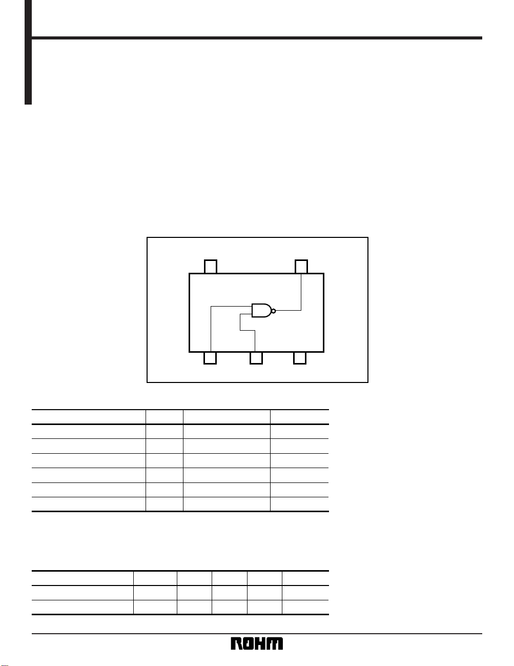
Single 2-input NAND gate
BU4S11
The BU4S11 is a dual-input positive logic NAND gate. This is an ultra-compact logic IC with one circuit of the
BU4011B built into an SMP package.
•
Features
1) Low current dissipation.
2) Super-mini mold package designed for surface
mounting.
3) Wide range of operating power supply voltage.
4) Capable of driving two L-TTL inputs and one LS-TTL
input directly
•
Block diagram
•
Recommended operating conditions (Ta = 25°C, VSS = 0 V)
Parameter Symbol Limits Unit
V
DD VSS – 0.3 ~ VSS + 18 V
Pd 170 mW
I
IN ± 10 mA
Topr – 40 ~ + 85 °C
Tstg – 55 ~ + 150 °C
V
IN VSS – 0.3 ~ VDD + 0.3 V
Power supply voltage
Power dissipation
Input current
Operating temperature
Storage temperature
Input voltage
Note 1: These values indicate the range limits of the voltage that can be applied to each pin without
destroying it. Operation cannot be guaranteed at these values.
Note 2: Power dissipation is reduced by 1.7mW for each increase in Ta of 1°C each 25°C.
Parameter Symbol Min. Typ. Max. Unit
V
DD 3 — 16 V
V
IN 0—VDD V
Power supply voltage
Input voltage
54
123
V
DD Y
ABV
SS
•
Absolute maximum ratings (Ta = 25°C)
Page 2
2
Standard ICs BS4S11
•
Electrical characteristics
DC characteristics (unless otherwise noted, V
SS = 0V, Ta = 25°C)
Parameter Symbol Min. Typ. Max. Unit
Measurement
circuit
V
DD (V)
V
IH
3.5 — — V 5
V
OUT = 0.5V
V
OUT = 1.0V
V
OUT = 1.5V
Fig.1
7.0 — — V 10
11.0 — — V 15
| I
OUT | < 1µA
V
IL
— — 1.5 V 5
V
OUT = 4.5V
V
OUT = 9.0V
V
OUT = 13.5V
— — 3.0 V 10
— — 4.0 V 15
| I
OUT | < 1µA
I
IH — — 0.3 µA15VIH = 15V
I
IL — — – 0.3 µA15VIL = 0V
V
OH
4.95 — — V 5
| I
OUT | < 1µA
V
IN = VSS
9.95 — — V 10
14.95 — — V 15
V
OL
— — 0.05 V 5
| I
OUT | < 1µA
V
IN = VDD
— — 0.05 V 10
— — 0.05 V 15
I
OH
– 0.51 — — mA 5 VOH = 4.6V
– 2.1 — — mA 5 V
OH = 2.5V
– 1.3 — — mA 10 V
OH = 9.5V
– 3.4 — — mA 15
V
OH = 13.5V
V
IN = VSS
IOL
0.51
——mA 5V
OL = 0.4V
1.3
— — mA 10 V
OL = 0.5V
3.4 — — mA 15
V
OL = 1.5V
V
IN = VDD
IDD
— — 0.25 µA5
V
IN = VSS, VDD— — 0.5 µA10
— — 1.0 µA15
Conditions
Input high level voltage
Input low level voltage
Input high level current
Input low level current
Output high level voltage
Output low level voltage
Output high level current
Output low level current
Static current dissipation
Page 3

3
Standard ICs BS4S11
Switching characteristics (unless otherwise noted, VSS = 0V, Ta = 25°C, CL = 50 pF)
Parameter Symbol Min. Typ. Max. Unit
Measurement
circuit
V
DD (V)
Conditions
t
TLH
— 70 — ns 5
—
Fig.2
— 35 — ns 10
— 30 — ns 15
t
THL
— 70 — ns 5
—— 35 — ns 10
— 30 — ns 15
t
PLH
— 85 — ns 5
—— 40 — ns 10
— 30 — ns 15
t
PHL
— 85 — ns 5
—— 40 — ns 10
— — ns 15
C
IN —5—pF 5 — —
30
Output rise time
Output fall time
Propagation delay time
Input capacitance
•
Measurement circuits
V
A
VDD
VSS
Fig.1 DC characteristics measurement circuit
VDD
P.G
C
L = 50pF
VSS
tTLH tTHL
20ns 20ns
90%
50%
10%
90%
50%
10%
tPHL
VOL
VSS
VDD
tPLH
VOH
Input waveform
Output waveform
Fig.2 Switching characteristics measurement circuit
Page 4
4
Standard ICs BS4S11
•
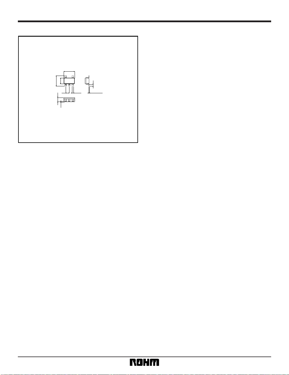
External dimensions (Units: mm)
SMP5
0.5
2.9 ± 0.2
1.6 ± 0.2
2.8 ± 0.3
0.4 ± 0.1
0.95
(5) (4)
(2)
(3)
1.1 ± 0.2
0.05
(1)
0.1
+ 0.1
– 0.05
 Loading...