

Page 1
Low voltage·High-accuracy detection
CMOS VOLTAGE DETECTOR IC
with delay time circuit
BU42XXFVE/F/G series
BU43XXFVE/F/G series
Description
ROHM's BU42XXFVE/F/G and BU43XXFVE/F/G series are low
voltage and high-accuracy detection type of VOLTAGE DETECTOR
ICs with built-in delay time circuit adopting CMOS process.
Low voltage of 0.9V detection can be realized. Adoption of highresistance process enable to reduce current consumption and to
set delay time by small capacitor.
Features
1) Detection voltage: 0.1V step line-up 0.9~4.8V (Typ.)
2) High-accuracy detection voltage: ±1.0% (Max.)
3) Low current consumption: 0.55µA typ. (Typ.) (VDET=4.8V, VDD=6.8V)
4) Excellent detection voltage temperature characteristic: ±30ppm/˚C
5) Delay time can be set by capacitor. (100msec: CT=0.015µF)
6) Open drain output (BU42XXseries), CMOS output (BU43XXseries)
7) Various package lineup
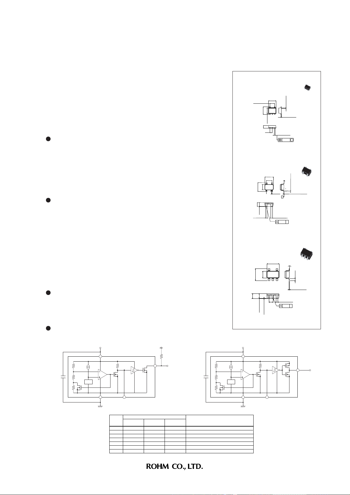
VSOF5 : (BU42XXFVE, BU43XXFVE)
SOP4 : (BU42XXF, BU43XXF)
SSOP5 : (BU42XXG, BU43XXG)
Application
Portable appliances with microcontroller and logic circuit
Application Circuit
BU42XXFVE
BU43XXFVE
1.0±0.05
BU42XXF
BU43XXF
2.1±0.2
1.05MAX
0.32±
BU42XXG
BU43XXG
2.8±0.2
1.25MAX
0.1
0.2
1.25±
0.9
0.05±0.05
0.05
0.04
0.2
1.6±
1.1±0.05
1.6±0.05
0.6Max.
2.0±0.2
±0.05
0.1
0.05±0.05
1.6±0.05
0.5
4
1
45
321
1.2±0.05
0.22±0.05
VSOF5
1.3
3
2
0.05
0.42
SOP4
2.9±0.2
5
4
1
2 3
0.95
SSOP5
0.2Max.
0.13±0.05
0.08
+5˚
4˚
-4˚
s
0.05
±
0.04
s
0.1
0.05
0.42
±
0.04
0.1
4˚
0.27±0.15
+6˚
-4˚
s
M
0.13
0.13
5
1
2
3
1pin : VOUT
2pin : SUB
3pin : CT
4pin : VDD
5pin : GND
4
1
2
0.05
±
0.03
1pin : GND
2pin : VDD
3pin : CT
4pin : VOUT
5
1
2
3
0.2Min.
0.05
±
0.03
1pin : VOUT
2pin : VDD
3pin : GND
4pin : N.C.
5pin : CT
4
3
4
(BU42XXFVE/F/G) BU43XXFVE/F/G
Vref
VDD
VDD
GND CT
Pin
name
Package
GND
VDD
CT
VOUT
N.C.
SUB
BU42XXF
BU43XXF
SOP4
1
2
3
4
-
- -
VDD
Vout
Pin number
BU42XXFVE
BU43XXFVE
VSOF5 SSOP5
5 3
4 2
3 5
1 1
2
Reset
BU42XXG
BU43XXG
4
Vref
Pin explanation
GND
Supply voltage
Capacitor connect pin for output delay time setting
Reset output
Non connection pin
Sub straight (Connect to VDD)
VDD
VDD
GND CT
Vout
Reset
Page 2
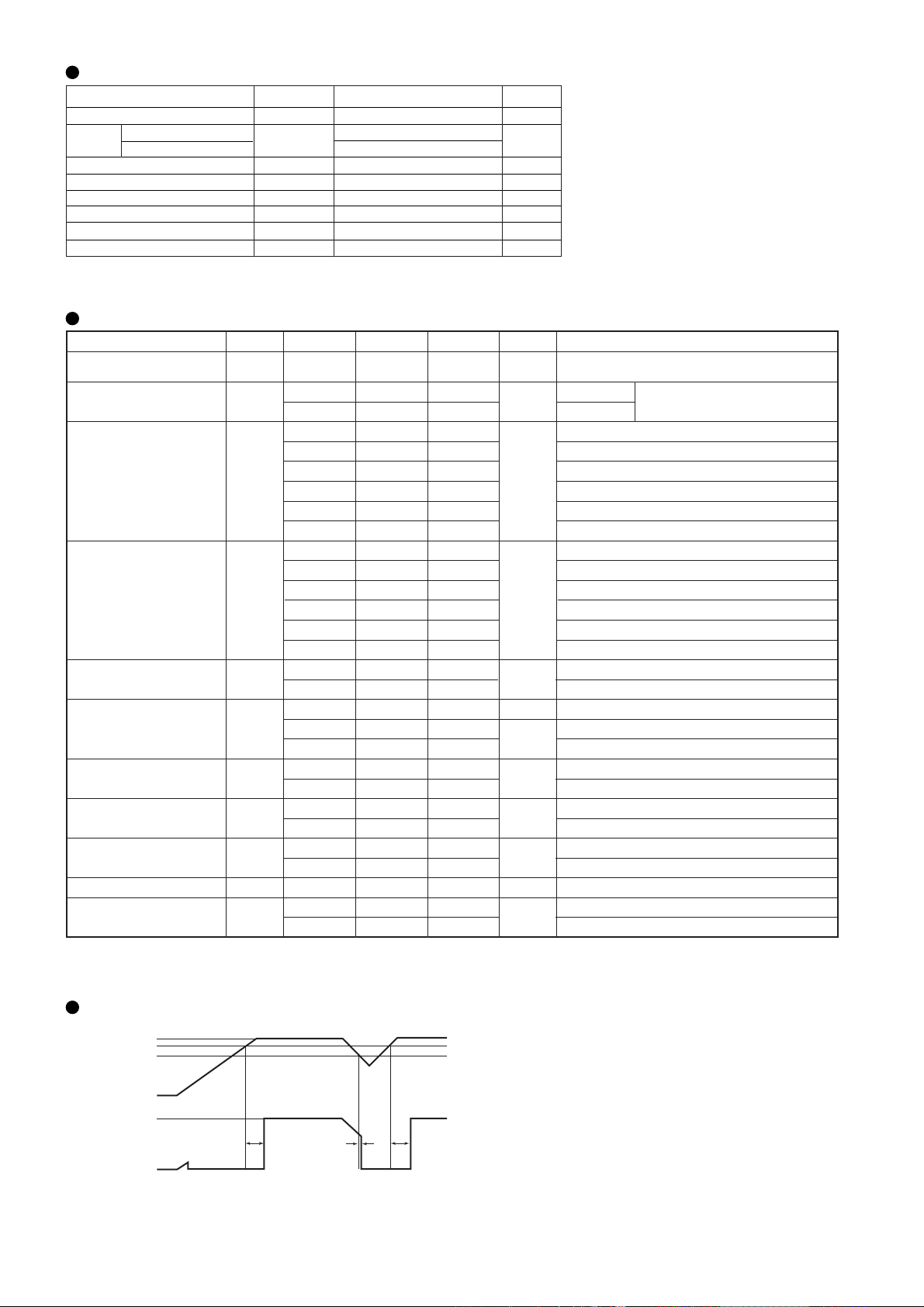
Absolute Maximum Ratings (Ta=25˚C)
Parameter Symbol Unit
Supply voltage
Output
voltage
CT pin input voltage
Power dissipation: VSOF5
Power dissipation: SOP4
Power dissipation: SSOP5
Operating temperature range
Storage temperature range
∗1 Derating : 2.1mW/˚C for operation above Ta=25˚C PCB (70mmx70mm, t=1.6mm) glass epoxy mounting.
∗2 Derating : 4.0mW/˚C for operation above Ta=25˚C PCB (70mmx70mm, t=1.6mm) glass epoxy mounting.
∗3 Derating : 5.4mW/˚C for operation above Ta=25˚C PCB (70mmx70mm, t=1.6mm) glass epoxy mounting.
Nch open drain output
CMOS output
VDD – GND
VOUT
VCT
∗1
Pd
2
∗
Pd
∗3
Pd
Topr
Tstg
GND – 0.3 ~ VDD + 0.3
GND – 0.3 ~ VDD + 0.3
Limits
– 0.3 ~ + 7
GND – 0.3 ~ + 7
210
400
540
– 40 ~ + 125
– 55 ~ + 125
V
V
V
mW
mW
mW
˚C
˚C
Electrical characteristics (Unless otherwise noted; Ta=
Parameter
Temperature coefficient
of detection voltage
Hysteresis voltage
Symbol Min. Max. Unit Conditions
∗4
VDET/∆T — ±30 — ppm/˚C
∆VDET
VDET × 0.03 VDET × 0.05 VDET × 0.08
VDET × 0.03 VDET × 0.05 VDET × 0.07
— 0.880.15
— 1.050.20
Circuit current ON
IDD1
— 1.230.25
— 1.400.30
— 1.580.35
— 1.750.40
— 1.40
— 1.58
Circuit current OFF
IDD2
— 1.75
— 1.93
— 2.10
—
Operating voltage range
VOPL
0.7 — —
0.9 — —
20 100 —
"L" output current (Nch)
IOL
1.0 3.3 —
4.0 7.2 —
"H" output current (Pch)
(BU43XX series only)
Output leak current
(BU42XX series only)
IOH
Ileak
CT pin
threshold voltage
∗4
CT pin output current
∗4 All shipment is not inspected for design guarantee.
Note) This product is not designed for protection against radioactive rays.
ICT
1.7 3.4 —
2.0 4.0 —
— 0 0.1
— 0 1
VDD × 0.35 VDD × 0.45
VDD × 0.40 VDD × 0.50 VDD × 0.60
9.0 10.0 11.0
5 40 —
200 400
Typ.
0.30
0.35
0.40
0.45
0.50
0.55 2.28
-
25°C ~ +125°C)
VDD × 0.55
—
V
=
>
VDET 1.1V
=
RL=470kΩ, VDD=L→H→L,
Ta=-40°C ~ +125°C
<
VDET 1.0V
VDD=VDET-0.2V, VDET=0.9~1.3V
VDET=1.4~2.1V
µA
VDET=2.2~2.7V
VDET=2.8~3.3V
VDET=3.4~4.2V
VDET=4.3~4.8V
VDD=VDET+2.0V, VDET=0.9~1.3V
VDET=1.4~2.1V
µA
VDET=2.2~2.7V
VDET=2.8~3.3V
VDET=3.4~4.2V
VDET=4.3~4.8V
<
VOL 0.4V, Ta=25°C ~ 125°C
V
µA
mA
mA
µA
VVCTH
=
<
VOL 0.4V, Ta=-25°C ~ +25°C
=
VDS=0.05V, VDD=0.85V
VDS=0.5V, VDD=1.5V, VDET=1.7V~4.8V
VDS=0.5V, VDD=2.4V, VDET=2.7V~4.8V
VDS=0.5V, VDD=4.8V, VDET=0.9V~3.9V
VDS=0.5V, VDD=6.0V, VDET=4.0V~4.8V
VDD=VDS=7V, Ta=-40°C ~ +85°C
VDD=VDS=7V, Ta=+85°C ~ +125°C
VDD=VDET×1.1, RL=470kΩ, Ta=25°C, VDET=0.9V~2.5V
VDD=VDET×1.1, RL=470kΩ, Ta=25°C, VDET=2.6V~4.8V
MΩRCTOutput delay resistance VDD=VDET×1.1, VCT=0.5V, Ta=25°C
VCT=0.1V, VDD=0.85V
µA
VCT=0.5V, VDD=1.5V, VDET=1.7V~4.8V
Timing chart and delay time setting
VDD
VDET + ∆VDET
VDET
VDD
0V
VOH
VOUT
VOL
tPLH tPLHtPHL
∗ Delay time setting (
tPLH = τ × RCT × CCT(Sec)
τ :
RCT(Ω) :
CCT(F) :
-
Reference
-
( τ × RCT) :
VDET = 0.9V ~ 2.5V
VDET = 2.6V ~ 4.8V
)
tPLH
Time constant
Designed to 10MΩ(Typ.) by resistance of the built-in IC
Capacitance of external capacitor
Capacitance of recommended CT capacitor is 100pF or more
Ta = 25°C
Ta = -25°C ~ 125°C
Ta = 25°C
Ta = -25°C ~ 125°C
(min : 5.1E6, typ. : 6.0E6, max. : 6.9E6)
(min : 3.3E6, typ. : 6.0E6, max. : 8.7E6)
(min : 5.9E6, typ. : 6.9E6, max. : 7.9E6)
(min : 3.8E6, typ. : 6.9E6, max. : 10.0E6)
Page 3
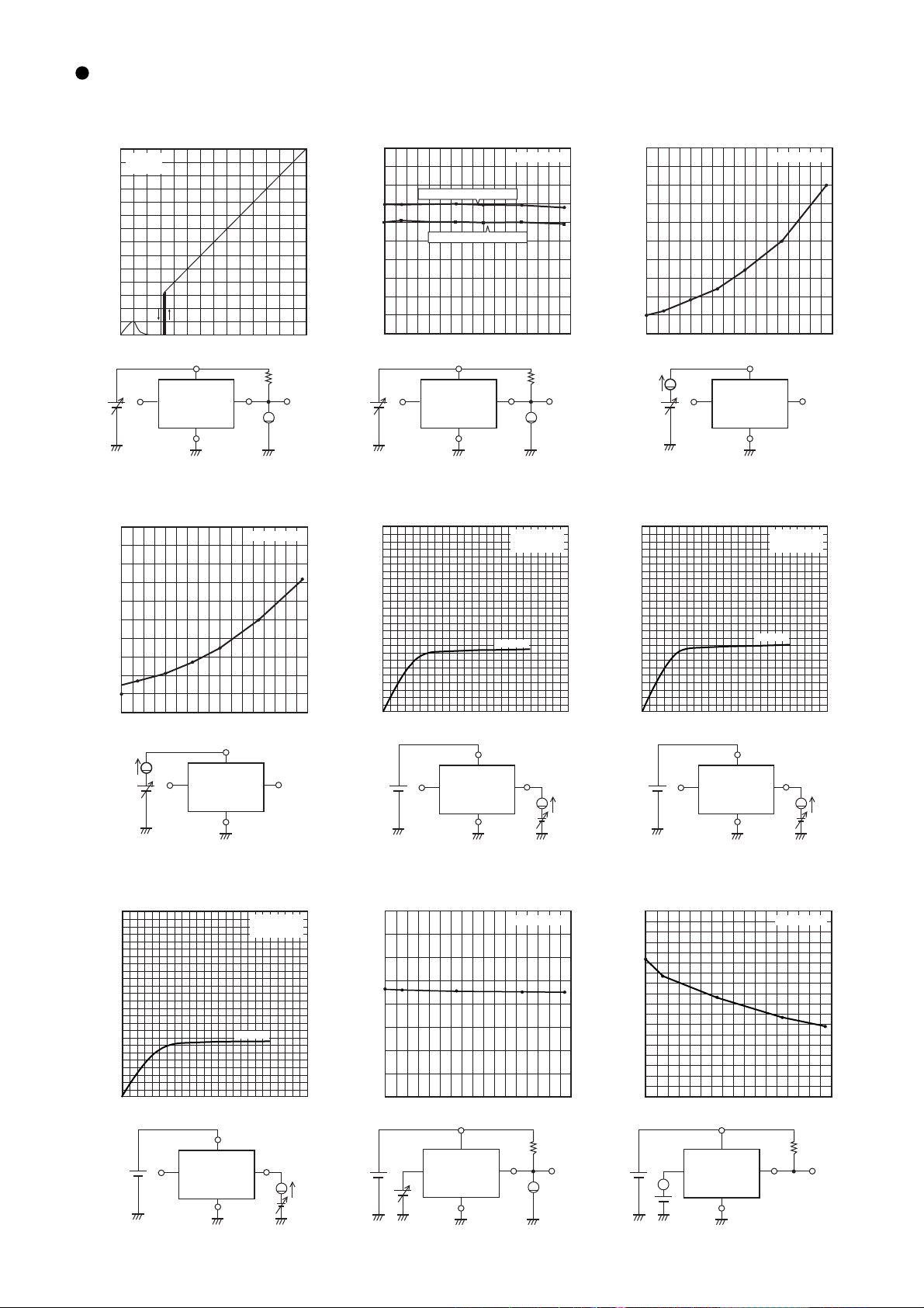
Characteristic chart and measurement circuit
I/O characteristic Detection voltage/Release voltage Circuit current when ON
VDD
[V]
VO
1.0
0.8
7
6
5
4
3
2
1
0
BU4216F
Vcc - Vo
2.0
(
low to high
VDET+∆VDET
1.5
[V]
VDET
1.0
-
3 54 7621
[V]
VCC
VDD
CT
VOUT
GND
RL=470KΩ
V
40 130100
VDD
high to low
0 50
Ta
VDD
CT
GND
[°C]
VOUT
(
VDET
[BU4216F]
)
)
RL=470KΩ
V
"L" output current [Ta=25°C]Circuit current when OFF
[BU4216F] [BU4216F]
5.0
Ta=25°C
4.0
0.5
0.4
0.3
[ µA ]
ICC
0.2
0.1
0
-
0 50
40 130100
Ta
A
VDD
CT
[BU4216F]
[°C]
VDD
VOUT
GND
"L" output current [Ta=-40°C]
5.0
4.0
[BU4216F]
Ta=-40°C
0.6
[ µA ]
ICC
0.4
0.2
0
-
0 50
40 130100
A
VDD
[°C]
Ta
VDD
CT
GND
VOUT
3.0
[mA]
IO
2.0
1.0
0.5 1
0
VDD
CT
Vcc=1.2V
1.5 2 2.5
[V]
VO
VDD
VOUT
GND
A
VDS
3.0
[mA]
IO
2.0
1.0
0.5 1
0
VDD
CT
Vcc=1.2V
1.5 2 2.5
[V]
VO
VDD
VOUT
GND
"L" output current [Ta=125°C] Threshold voltage CT pin circuit resistance
5.0
4.0
3.0
[mA]
IO
2.0
1.0
0.5 1
0
VO
[BU4216F]
Ta=125°C
Vcc=1.2V
1.5 2 2.5
[V]
1.00
0.95
0.90
0.85
0.80
[V]
CT
0.75
0.70
0.65
0.60
-
0 50
40 130100
[°C]
Ta
[BU4216F]
18
16
14
12
10
[V]
8
RCT
6
4
2
0
-
0 50
40 130100
[°C]
Ta
[BU4216F]
A
VDS
VDD
VDD
GND
VOUT
VDD
A
VDS
VCT
CT
VDD
CT
VOUT
GND
RL=470KΩ
V
VDD
VDD
CT
A
VCT
VOUT
GND
RL=470KΩ
Page 4
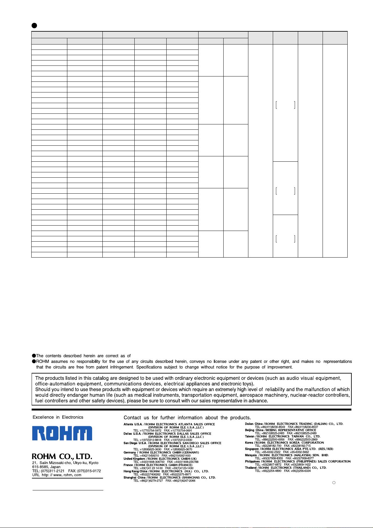
Series lineup
Open drain output CMOS output
BU4248G/FVE/F
BU4247G/FVE/F
BU4246G/FVE/F
BU4245G/FVE/F
BU4244G/FVE/F
BU4243G/FVE/F
BU4242G/FVE/F
BU4241G/FVE/F
BU4240G/FVE/F
BU4239G/FVE/F
BU4238G/FVE/F
BU4237G/FVE/F
BU4236G/FVE/F
BU4235G/FVE/F
BU4234G/FVE/F
BU4233G/FVE/F
BU4232G/FVE/F
BU4231G/FVE/F
BU4230G/FVE/F
BU4229G/FVE/F
BU4228G/FVE/F
BU4227G/FVE/F
BU4226G/FVE/F
BU4225G/FVE/F
BU4224G/FVE/F
BU4223G/FVE/F
BU4222G/FVE/F
BU4221G/FVE/F
BU4220G/FVE/F
BU4219G/FVE/F
BU4218G/FVE/F
BU4217G/FVE/F
BU4216G/FVE/F
BU4215G/FVE/F
BU4214G/FVE/F
BU4213G/FVE/F
BU4212G/FVE/F
BU4211G/FVE/F
BU4210G/FVE/F
BU4209G/FVE/F
Part No.
BU4348G/FVE/F
BU4347G/FVE/F
BU4346G/FVE/F
BU4345G/FVE/F
BU4344G/FVE/F
BU4343G/FVE/F
BU4342G/FVE/F
BU4341G/FVE/F
BU4340G/FVE/F
BU4339G/FVE/F
BU4338G/FVE/F
BU4337G/FVE/F
BU4336G/FVE/F
BU4335G/FVE/F
BU4334G/FVE/F
BU4333G/FVE/F
BU4332G/FVE/F
BU4331G/FVE/F
BU4330G/FVE/F
BU4329G/FVE/F
BU4328G/FVE/F
BU4327G/FVE/F
BU4326G/FVE/F
BU4325G/FVE/F
BU4324G/FVE/F
BU4323G/FVE/F
BU4322G/FVE/F
BU4321G/FVE/F
BU4320G/FVE/F
BU4319G/FVE/F
BU4318G/FVE/F
BU4317G/FVE/F
BU4316G/FVE/F
BU4315G/FVE/F
BU4314G/FVE/F
BU4313G/FVE/F
BU4312G/FVE/F
BU4311G/FVE/F
BU4310G/FVE/F
BU4309G/FVE/F
Detection voltage VDET (V)
4.752
4.653
4.554
4.455
4.356
4.257
4.158
4.059
3.960
3.861
3.762
3.663
3.564
3.465
3.366
3.267
3.168
3.069
2.970
2.871
2.772
2.673
2.574
2.475
2.376
2.277
2.178
2.079
1.980
1.881
1.782
1.683
1.584
1.485
1.386
1.287
1.188
1.089
0.990
0.891
Typ.Min.
4.800
4.700
4.600
4.500
4.400
4.300
4.200
4.100
4.000
3.900
3.800
3.700
3.600
3.500
3.400
3.300
3.200
3.100
3.000
2.900
2.800
2.700
2.600
2.500
2.400
2.300
2.200
2.100
2.000
1.900
1.800
1.700
1.600
1.500
1.400
1.300
1.200
1.100
1.000
0.900
Max.
4.848
4.747
4.646
4.545
4.444
4.343
4.242
4.141
4.040
3.939
3.838
3.737
3.636
3.535
3.434
3.333
3.232
3.131
3.030
2.929
2.828
2.727
2.626
2.525
2.424
2.323
2.222
2.121
2.020
1.919
1.818
1.717
1.616
1.515
1.414
1.313
1.212
1.111
1.010
0.909
Circuit current (µA Typ.)
ON
OFF
0.40 0.55
0.35 0.50
0.30 0.45
0.25
0.40
0.20 0.35
0.300.15
Hysteresis
voltage
( V, Typ. )
VDET×0.05
“L”output
current
(Typ.)
7.2mA
VDD=2.4V
VDS=0.5V
3.3mA
VDD=1.5V
VDS=0.5V
100µA
VDD=0.85V
VDS=0.05V
Delay circuit
resistance
(MΩ)Typ.
10.0
Package
SSOP5
⁄
VSOF5
⁄
SOP4
Published by
LSI Application Engineering Group
July, 2004
Catalog NO.04P092A '04.7 ROHM 5000 KW
C
Page 5

Appendix
No technical content pages of this document may be reproduced in any form or transmitted by any
means without prior permission of ROHM CO.,LTD.
The contents described herein are subject to change without notice. The specifications for the
product described in this document are for reference only. Upon actual use, therefore, please request
that specifications to be separately delivered.
Application circuit diagrams and circuit constants contained herein are shown as examples of standard
use and operation. Please pay careful attention to the peripheral conditions when designing circuits
and deciding upon circuit constants in the set.
Any data, including, but not limited to application circuit diagrams information, described herein
are intended only as illustrations of such devices and not as the specifications for such devices. ROHM
CO.,LTD. disclaims any warranty that any use of such devices shall be free from infringement of any
third party's intellectual property rights or other proprietary rights, and further, assumes no liability of
whatsoever nature in the event of any such infringement, or arising from or connected with or related
to the use of such devices.
Upon the sale of any such devices, other than for buyer's right to use such devices itself, resell or
otherwise dispose of the same, no express or implied right or license to practice or commercially
exploit any intellectual property rights or other proprietary rights owned or controlled by
ROHM CO., LTD. is granted to any such buyer.
Products listed in this document are no antiradiation design.
Notes
The products listed in this document are designed to be used with ordinary electronic equipment or devices
(such as audio visual equipment, office-automation equipment, communications devices, electrical
appliances and electronic toys).
Should you intend to use these products with equipment or devices which require an extremely high level of
reliability and the malfunction of with would directly endanger human life (such as medical instruments,
transportation equipment, aerospace machinery, nuclear-reactor controllers, fuel controllers and other
safety devices), please be sure to consult with our sales representative in advance.
About Export Control Order in Japan
Products described herein are the objects of controlled goods in Annex 1 (Item 16) of Export Trade Control
Order in Japan.
In case of export from Japan, please confirm if it applies to "objective" criteria or an "informed" (by MITI clause)
on the basis of "catch all controls for Non-Proliferation of Weapons of Mass Destruction.
Appendix1-Rev1.1
 Loading...