

Page 1
1
Standard ICs
BCD-to-decimal decoder
BU4028B
The BU4028B is a decoder which converts BCD signals to decimal signals.
Of the ten outputs Q
0 to Q9, those corresponding to the A to D input codes are set to “H”, and the others are all set to
“L”.
If inputs A to C are used and input D is used as disabled input, the BU4028B can also be used as a 1-of-8 decoder.
•
Features
1) Low power dissipation.
2) Wide range of operating power supply voltages.
3) High input impedance.
4) High fan-out.
5) Direct drive of 2 L-TTL inputs and 1LS-TTL input.
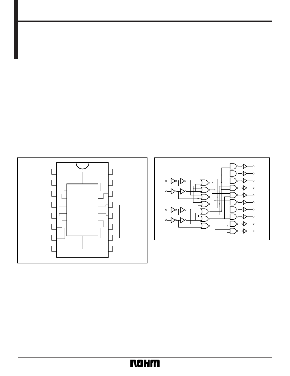
•
Block diagram
Q2
Q4
Q8
Q7
Q9
Q5
Q6
Q0
B
C
D
A
Q
1
Q3
2
Q
2
Q4
Q7
Q9
Q5
Q6
Q0
3
4
5
6
7
8
15
14
13
12
11
10
9
V
SS
1
V
DD
B
C
IN
D
A
Q
1
Q3
Q8
16
•
Logic circuit diagram
A
B
C
D
Q0
Q1
Q2
Q3
Q4
Q5
Q6
Q7
Q8
Q9
Page 2
2
Standard ICs BA4028B
•
Absolute maximum ratings (Ta = 25°C, VSS = 0V)
Parameter Symbol Limits Unit
Power supply voltage V
DD V
Power dissipation mW
Operating temperature – 40 ~ + 85
°C
Storage temperature – 55 ~ + 150 °C
Input voltage V
IN – 0.3 ~ VDD + 0.3 V
– 0.3 ~ + 18
1000 (DIP)Pd
Topr
Tstg
•
Truth table
INPUT OUTPUT
DCBAQ
9 Q8 Q7 Q6 Q5 Q4 Q3 Q2 Q1 Q0
L
L
L
L
L
L
L
L
L
L
H
H
L
H
L
H
L
L
L
L
L
L
L
L
L
L
L
L
L
L
L
L
L
L
L
L
L
L
L
L
L
L
L
H
L
L
H
L
L
H
L
L
H
L
L
L
L
L
L
L
H
H
H
H
L
L
H
H
L
H
L
H
L
L
L
L
L
L
L
L
L
L
L
H
L
L
H
L
L
H
L
L
H
L
L
L
L
L
L
L
L
L
L
L
L
L
L
L
L
L
L
L
H
H
H
H
L
L
L
L
L
L
H
H
L
H
L
H
L
H
L
L
H
L
L
L
L
L
L
L
L
L
L
L
L
L
L
L
L
L
L
L
L
L
L
L
L
L
L
L
L
L
L
L
L
L
L
L
H
H
H
H
H
H
H
H
L
L
H
H
L
H
L
H
L
L
L
L
L
L
L
L
L
L
L
L
L
L
L
L
L
L
L
L
L
L
L
L
L
L
L
L
L
L
L
L
L
L
L
L
L
L
L
L
Page 3

3
Standard ICs BA4028B
Parameter Symbol Min. Typ. Max. Unit Conditions
V
DD
(V)
Input high level voltage
V
IH
3.5
——
V
5
—
Fig.17.0
——
10
11.0
——
15
Input low level voltage
V
IL
——
1.5
V
5
—
Fig.1
——
3.0 10
——
4.0 15
Input high level current
I
IH
——
0.3
µ
A15V
IH
=
15V Fig.1
Input low level current
I
IL
— — –
0.3
µ
A15V
IL
=
0V Fig.1
Output high level voltage
V
OH
4.95
——
V
5
Fig.19.95
——
10
14.95
——
15
Output low level voltage
V
OL
——
0.05
V
5
I
O
=
0mA Fig.1
——
0.05 10
——
0.05 15
Output high level current
I
OH
–
0.16
——
mA
5V
OH
=
4.6V
Fig.1
–
0.4
——
10 VOH =
9.5V
–
1.2
——
15 VOH =
13.5V
Output low level current
I
OL
0.44
——
mA
5V
OL
=
0.4V
FIg.11.1
——
10 VOL =
0.5V
3.0
——
15 VOL =
1.5V
Static current dissipation
I
DD
——
1
µ
A
5
VI =
VDD or GND
———
210
——
415
I
O
=
0mA
Measurement
circuit
•
Electrical characteristics
DC characteristics (unless otherwise noted, Ta = 25°C, V
SS = 0V)
Page 4

4
Standard ICs BA4028B
Switching characteristics (Ta = 25°C, CL = 50pF, VSS = 0V)
Parameter Symbol Min. Typ. Max. Unit Conditions
Measurement
circuit
t
TLH
—
180
—
ns
5
—
Fig.2, 3
—
90
—
10
—
65
—
15
t
THL
—
100
—
ns
5
—
Fig.2, 3
—
50
—
10
—
40
—
15
“L” to “H” propagation delay time
t
PLH
—
300
—
ns
5
—
Fig.2, 3
—
130
—
10
—
90
—
15
“H” to “L” propagation delay time
t
PHL
—
300
—
ns
5
—
Fig.2, 3
—
130
—
10
—
90
—
15
Input capacitance C
IN
—
5
—
pF
—— —
V
DD
(V)
Output rise time
Output fall time
Page 5

5
Standard ICs BA4028B
•
Measurement circuits
VDD
VDD
VSS
VSS
VIN
TABLE
3
Q
0
A
10
16
B
13
C
12
D
11
14
Q
1
2
Q
2
15
Q
3
1
Q
4
6
Q
5
7
Q
6
4
Q
7
9
Q
8
5
Q
9
Fig. 1 DC characteristics measurement circuit
TEST
NO.
INPUT OUTPUT
A B C D Pos. Neg.
1V
IN VSS VSS VSS Q1 Q0
Q6 Q4
Q7 Q3
Q9 Q1
Q2 Q0
Q5 Q1
Q8 Q0
Q4 Q0
Q3 Q2
2VSS VIN VDD VSS
3VDD VDD VIN VSS
4VDD VSS VSS VIN
5VSS VIN VSS VSS
6VDD VSS VIN VSS
7VSS VSS VSS VIN
8VSS VSS VIN VSS
9VIN VDD VSS VSS
VIN
OUTPUT
Pos.
OUTPUT
Neg.
VDD
TABLE
3
A
10
16
B
13
C
12
D
11
14
2
15
1
6
7
4
9
5
P.G.
Note: Connect C
L = 50pF to each output pin.
8
VDD
VSS
VSS
Q0
Q1
Q2
Q3
Q4
Q5
Q6
Q7
Q8
Q9
Fig. 2 Switching characteristics measurement circuit
90%
50%
10%
20ns 20ns
90%
50%
10%
tPHL
VDD
Input
GND
Neg.
Pos.
Output
t
THL
tPLH
tTLH
Fig. 3 Switching time test waveform
TEST
NO.
INPUT OUTPUT
A B C D Pos. Neg.
1
2
3
4
5
6
7
8
9
P.G. V
SS VSS VSS Q1 Q0
Q6 Q4
Q7 Q3
Q9 Q1
Q2 Q0
Q5 Q1
Q8 Q0
Q4 Q0
Q3 Q2
VSS P.G. VDD VSS
VDD VDD P.G. VSS
VDD VSS VSS P.G.
V
SS P.G. VSS VSS
VDD VSS P.G. VSS
VSS VSS VSS P.G.
V
SS VSS P.G. VSS
P.G. VDD VSS VSS
Page 6

6
Standard ICs BA4028B
•
Electrical characteristics curve
POWER DISSIPATION: Pd (mW)
1200
1000
800
600
400
200
0
0255075100125150
AMBIENT TEMPERATURE: Ta (°C)
Fig.4 Power dissipation vs. Ta
•
External dimensions (Units: mm)
DIP16
0.51Min.
0.3
± 0.1
916
81
6.5 ± 0.3
3.2
±
0.2
4.25
±
0.3
0.5 ± 0.1
19.4 ± 0.3
2.54
0° ~ 15°
7.62
 Loading...