

Page 1
®
Rayson Bluetooth
Module
BC03/04-audio Class2 Module BTM-350
Features Outline
The module is a Max.4dBm( Class2 ) module.
Bluetooth standard Ver. 2.0 conformity.
Low current consumption :
Park, Sniff, Hold and Deep Sleep
2.2v to 3.6V operation
Built-in 15-bit Linear Audio Codec
Embedded 6Mbit Flash/ROM Memory
Integrated 32Kbits EEPROM
Integrated Switch-mode Regulator
Integrated Battery Charger with programmable current
Interface: USB,UART&PCM(for voice CODEC)
HCI or Headset,Gateway,SPP firmware is available
Small outline. 16.5 x 13 x 2.2 mm
Applications
z Notebook PC,PDA
z Cellular Phone
z Cordless headset
z Domestic and industrial applications
z Headsets
z Automotive hands-free kits
z General purpose Bluetooth system requiring an
On-chip CODEC
Electrical Characteristics
Absolute Maximum Ratings
Ratings Min. Max.
Storage Temperature
Supply Voltage VDD -0.4 V 3.7 V
Recommended Operating Condition
Operating Condition Min. Max.
Operating Temperature range
Supply Voltage VDD 3.0 V 3.6 V
Power Consumption: VDD=1.8V Temperature=+20℃ Output power=+4dBm
Mode Average Unit
SCO connection HV3(no sniff mode)(slave)
SCO connection HV1 (master) (slave) 37.6 mA
ACL data transfer 921kpbs UART (slave) 30.9 mA
Standby mode (connected to host, no RF activity) 0.10 mA
-40 ℃ +150 ℃
-20 ℃ +85 ℃
24.2 mA
Parked slave, 1.28s beacon interval, 38.4kbps UART 0.28 mA
Reset(RESETB low) 57 uA
CODEC
Microphone input and ADC 0.85 mA
DAC and loudspeaker driver, no signal 1.4 mA
Page 2
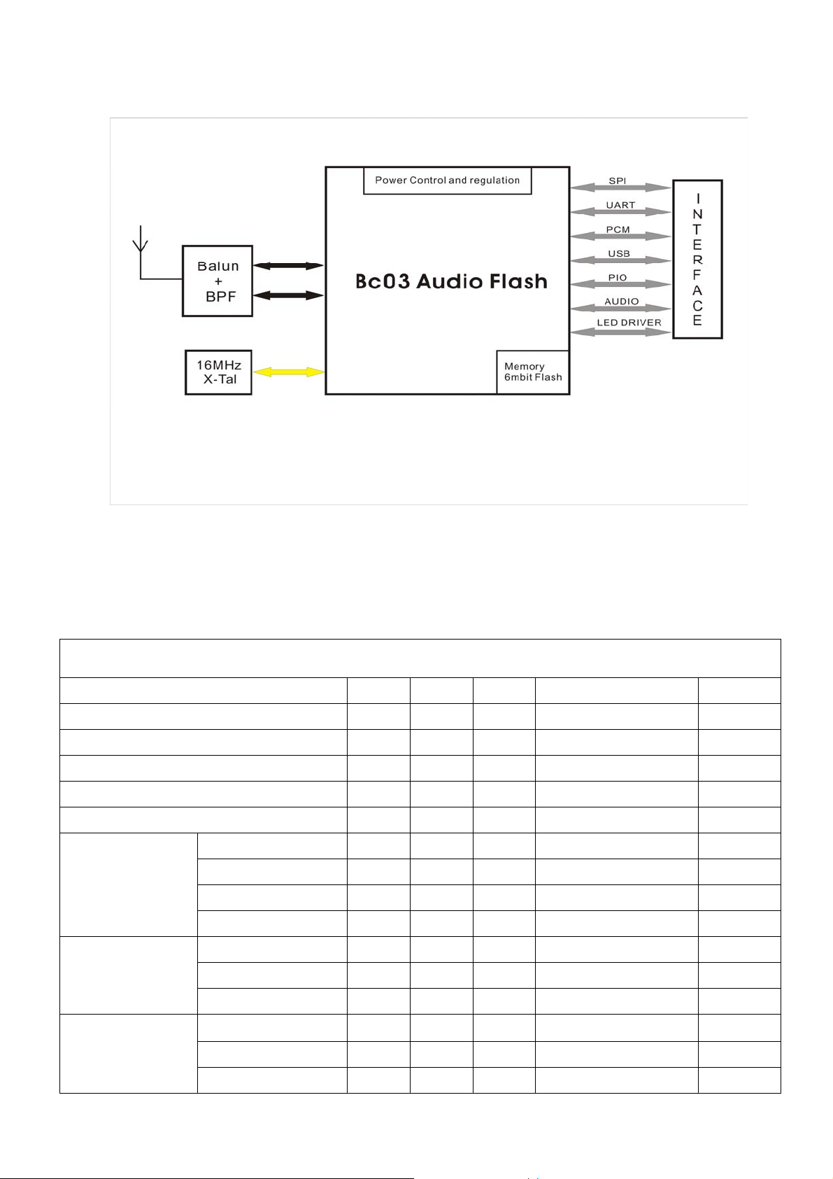
Block Diagram
Radio Characteristics:VDD=1.8V Temperature=+20℃
Transmitter Performance
Parameter Min. Type Max. Bluetooth Spec. Unit
RF transmit power - 2 - -6 to +4 dBm
RF power control range - 35 RF power range control resolution - 0.5 -
20dB bandwidth for modulated carrier - 820 Initial carrier frequency tolerance - 3.0 -
Drift Rate - 8.0 -
Carrier frequency
drift
DH1 - 8.0 DH3 - 9.0 -
≥16
≤1000
±75
±20
±24
±40
KHz
KHz
KHz/50uS
KHz
KHz
Adjacent
characteristic
Modulation
characteristic
DH5 - 10 +/- 2 MHz - -45 +/- 3 MHz - -48 +/- 4MHz -
△F1avg
△F2avg
△F1avg/△F1avg
- 165 -
- 151 - 115 KHz
- 0.99 -
<-50
140≤△F1avg≤175
±40
≤- 20
≤- 40
≤- 40
≥0.8
KHz
dBm
dBm
dBm
KHz
Page 3

Receiver Performance
Parameter Frequency
Min. Type Max. Bluetooth Spec. Unit
(GHz)
Sensitivity at 0.1% BER
for all packet types
Maximum receive signal at 0.1% BER -20
C/I performance
Adjacent channel
sensitivity
Max. level of intermodulation interferers - -27 -
Spurious output level -
2402 - -84 - dBm
2441 - -82 - dBm
2480 - -85 -
>0
C/I co-channel - 10 F=F0+1MHz - -2 F=F0-1MHz - 0 F=F0+2MHz - -38 F=F0-2MHz - -22 F=F0+3MHz - -50 F=F0-5MHz - -50 F=F
-
image
-27
<-150
-
-
- dBm/Hz
≤- 70
≥- 20
≤11
≤0
≤0
≤- 30
≤- 20
≤- 40
≤- 40
≤- 9
≥- 39
dBm
dBm
dB
dB
dB
dB
dB
dB
dB
dB
dBm
Page 4

BTM-350 Pins Function
No. Pin Name Pin Type Pin description
1 GND GND Common ground
2 RF_IO Analogue Antenna interface
3 GND GND Common ground
4 PIO[0] Bi-directional Programmable I/O terminal, RX Enable
5 PIO[1] Bi-directional Programmable I/O terminal, TX Enable
6 PIO[2] Bi-directional Programmable I/O terminal, external CLK_REQ
7 PIO[3] Bi-directional Programmable I/O terminal
8 SPK_N Analogue Speaker ou tput negative
9 SPK_P Analogue Speaker ou tput positive
11 MIC_N Analogue Microphone input negative
10 MIC_P Analogue Microphone input positive
12 GND GND Common ground
13
14 VREG_EN CMOS input Internal Regulator enable control input
15 AIO[0] Bi-directional Programmable Input/Output Line
16 AIO[1] Bi-directional Programmable Input/Output Line
17 UART_RTS CMOS output UART request to send(active low)
18 UART_TX CMOS output UART data output
NC No Connection Reserved
19 UART_RX CMOS input UART data input
20 UART_CTS CMOS input UART clear to send(active low)
21
22
23
24
25
26
27
28
29
30
31
32
33
34 VBAT
35
36
37
38
39 1.8V P ower 1.8V Internal Power Output
40
41
42
PIO[4] Bi-directional Programmable I/O terminal
USB_DN Bi-directional USB data minus
USB_DP Bi-directional USB data plus
PCM_IN CMOS input Synchronous data input
PCM_SYNC Bi-directional Synchronous data sync
PCM_CLK Bi-directional Synchronous data clock
PCM_OUT CMOS output Synchronous data output
PIO[5]
RESETB CMOS input
SPI_CLK CMOS input Serial Peripheral Interface clock
SPI_MISO CMOS output Serial Peripheral Interface data output
V_CHG Power Lithium lion battery charger input
GND GND Common ground
SPI_MOSI CMOS input Serial Peripheral Interface data input
SPI_CSB CMOS input Chip select for Synchronous Serial Interface(active low)
LED[1] Open drain output Current sink to drive LED
LED[0] Open drain output Current sink to drive LED
PIO[9]
PIO[10] Bi-directional Programmable I/O terminal
PIO[11] Bi-directional Programmable I/O terminal
Bi-directional Programmable I/O terminal
Reset input (Active low)
Power Battery power input
Bi-directional Programmable I/O terminal
Page 5

Dimension
Unit:mm
TOP VIEW
Bottom View
Design to Micro
Strip Line
PCB LAYOUT(Top View)
Page 6

Headset Application
 Loading...