

Page 1
®
Rayson’s Bluetooth
Module
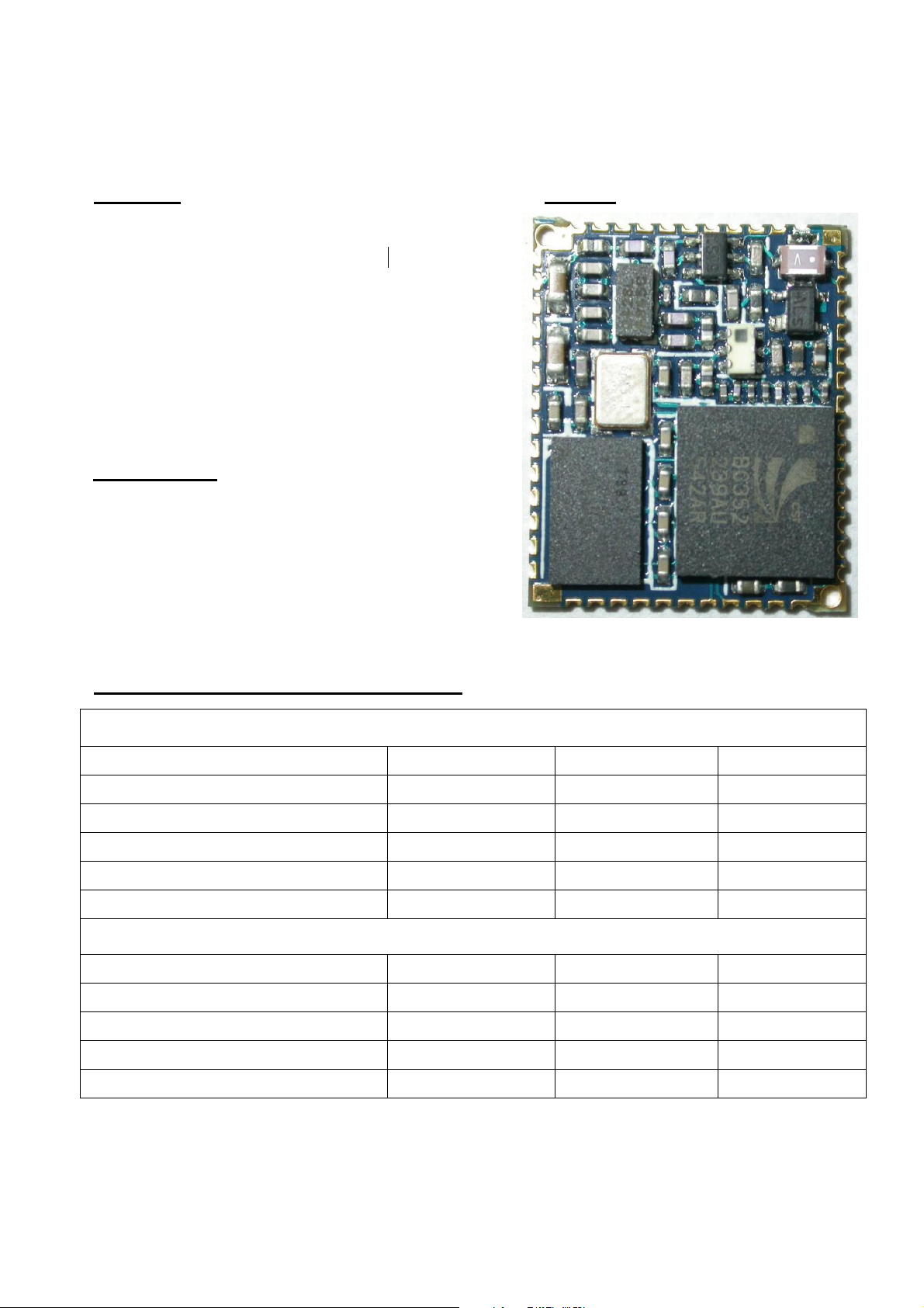
BC03-mm Class1 Stereo Module BTM-240/250
Features Outline
The module is a Max.18dBm( Class1 ) module.
Bluetooth standard Ver. 2.0 conformity.
Low current consumption
3.0V or 1.8V operation
Embedded Kalimba DSP Co-Processor
Integrated 16-bit Stereo Audio CODEC
Scatternet Support
Interface: USB,UART&PCM(for voice CODEC)
Support Digital Audio Bus : I
Headset/Handsfree firmware is available
A2DP/AVRCP profile support
RoHS compliant
Small outline. 16 x 14 x 2.0 mm
Applications
z Cellular Phone
z Cordless headset
z Echo Cancellation
z Stereo headphones
z Enhance Audio application
z Automotive Hands-free Kits
z High performance telephone headsets
2
S or SPDIF
General Electrical Specification
Absolute Maximum Ratings
Parameter Min. Max. Unit
Storage Temperature -40 +150 ℃
Supply Voltage(VDD 3.3V, BTM-240) -0.4 3.7 DCV
Supply Voltage(VDD 1.8V, BTM-250) -0.4 2.2 DCV
Supply Voltage(PA) -0.4 3.7 DCV
Other Pin Voltage Vss-0.4 VDD+0.4 DCV
Recommended Operating Conditions
Parameter Min. Max. Unit
Operating Temperature -20 +85 ℃
Supply Voltage(VDD 3.3V, BTM-240) 2.7 3.6 DCV
Supply Voltage(VDD 1.8V, BTM-250) 1.7 1.9 DCV
Supply Voltage(PA) 3.0 3.6 DCV
Page 2
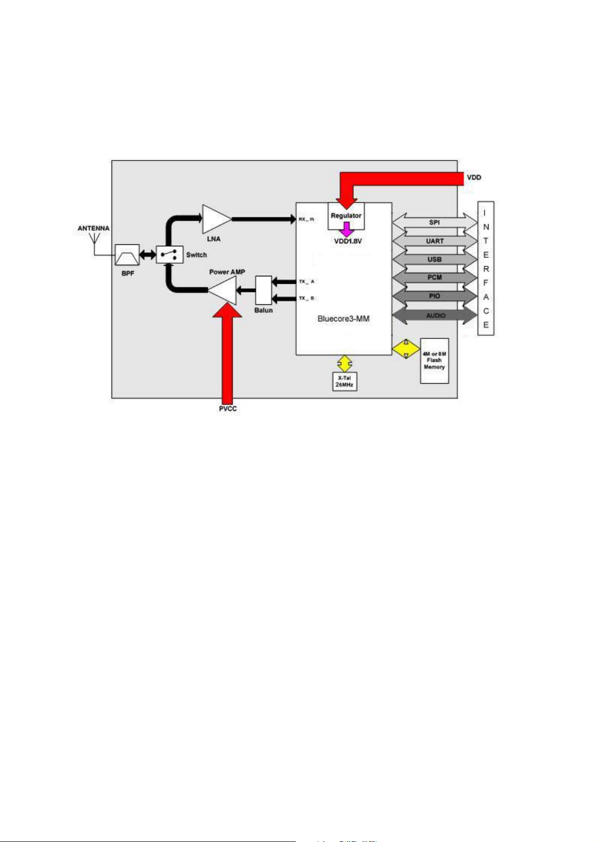
Block Diagram
Page 3

RF Specification: VDD=1.8V Temperature=+20℃
Transmitter Performance
Parameter Min. Type Max. Bluetooth Spec. Unit
RF transmit power - 17 - 0 to +20 dBm
RF power control range - 20 RF power range control resolution - 0.5 -
20dB bandwidth for modulated carrier - 720 Initial carrier frequency tolerance - 2.0 -
Drift Rate - 8.0 -
Carrier frequency
drift
Adjacent
characteristic
Modulation
characteristic
DH1 - 8.0 DH3 - 9.0 DH5 - 10 +/- 2 MHz - -40 +/- 3 MHz - -47 +/- 4MHz - -50 -
△F1avg
△F2avg
△F1avg/△F1avg
- 166 -
- 157 - 115 KHz
- 0.97 -
140≤△F1avg≤175
≥16
≤1000
±75
±20
±24
±40
±40
≤- 20
≤- 40
≤- 40
≥0.8
KHz
KHz
KHz/50uS
KHz
KHz
KHz
dBm
dBm
dBm
KHz
Receiver Performance
Parameter Frequency
Min. Type Max. Bluetooth Spec. Unit
(GHz)
Sensitivity at 0.1%
BER for all packet
types
Maximum receive signal at 0.1% BER - -10 -
C/I performance
Adjacent channel
sensitivity
Max. level of intermodulation
interferers
Spurious output level - -142 - dBm/Hz
2402 - -88 - dBm
2441 - -88 - dBm
2480 - -88 -
C/I co-channel - 9 F=F0+1MHz - -3 F=F0-1MHz - -7 F=F0+2MHz - -41 F=F0-2MHz - -42 F=F0+3MHz - -43 F=F0-5MHz - -42 F=F
image
- -22 -
- -27 -
≤- 70
≥- 20
≤11
≤0
≤0
≤- 30
≤- 20
≤- 40
≤- 40
≤- 9
≥- 39
dBm
dBm
dB
dB
dB
dB
dB
dB
dB
dB
dBm
Page 4

BTM-240/250 Pin Functions
_
g
)
)
)
)
)
A
(
VDD_
)
)
K
/SCK
A
PIN NAME TYPE FUNCTION
1 GND GND Ground
2 PIO(0) Bi-directional Programmable Input / Output Line
3
4 AUDIO_IN_LN Analogue Microphone & Audio Signal input negative(Left channel
5 AUDIO_IN_RP Analogue Microphone & Audio Signal input positive(Right channel
6 AUDIO_IN_RN Analogue Microphone & Audio Signal inputnegative(Right channel
7 AUDIO_OUT_RN Analogue Speaker & Audio Signal output negative(Right channel
8 AUDIO_OUT_RP Analogue Speaker & Audio Signal output positive(Right channel)
9 AUDIO_OUT_LN Analogue Speaker & Audio Signal output negative(Left channel)
10 AUDIO_OUT_LP Analogue Speaker & Audio Signal output positive(Left channel)
11 GND GND Ground
12 GND GND Ground
13 +V_PA Power Power supply for P
14 +1V8 Power Leave open, when VDD_IN 1.8V operate, please wire with VDD_IN
15
16 NC Reserved
17 AIO0 Bi-directional ADC/DAC Input/Output Line
18 AIO1 Bi-directional ADC/DACInput/Output Line, Battery Monitor Input
19 AIO3 Bi-directional ADC/DAC Input/Output Line
20 PCM_SYNC/WS Bi-directional Synchronous Data Sync / I2S ws (typically SCK=64*WS
21 PCM_IN/SD_IN CMOS Input Synchronous Data Input / I2S serial data in
22 PCM_OUT/SD_OUT CMOS Output Synchronous Data Output / I2S serial data out
23 PCM_CL
24 UART_CTS CMOS Input UART Clear To Send (Active Low)
25 UART_RTS CMOS Output UART Request To Send (Active Low)
26 UART_RX CMOS Input UART Data Input
27 UART_TX CMOS Output UART Data Output
28 PIO(4) Bi-directional Programmable Input / Output Line
29 PIO(5) Bi-directional Programmable Input/Output line
30 PIO(6) Bi-directional Programmable Input/Output line
31 PIO(7) Bi-directional Programmable Input/Output line
32 USB_DP Bi-directional USB Data Plus
33 USB_DN Bi-directional USB Data Minus
34 SPI_MOSI CMOS Input Serial Peripheral Interface Data Input
35 SPI_CSB CMOS Input Chip Select For Synchronous Serial Interface active low
36 GND GND Ground
37 GND GND Ground
38 SPI_CLK CMOS Input Serial Peripheral Interface Clock
39 SPI_MISO CMOS Output Serial Peripheral Interface Data Output
40 RESET CMOS Input Reset if high. must be high for >5ms to cause a reset
41 PIO(8) Bi-directional Programmable Input/Output Line
42 PIO(9) Bi-directional Programmable Input/Output Line
43 PIO(10) Bi-directional Programmable Input/Output Line
44 PIO(11) Bi-directional Programmable Input/Output Line
45 PIO(3) Bi-directional Programmable Input/Output Line
46 PIO(2) Bi-directional Programmable Input / Output Line
47 PIO(1) Bi-directional Programmable Input/Output Line
48 GND GND Ground
49 RF_IO Analogue
50 GND GND Ground
AUDIO
IN_LP
IN Power Power Input (normal 3.3V
Analo
Bi-directional Synchronous Data Clock / I2S serial data clock
ue Microphone & Audio Signal input positive(Left channel
recommend 3.3V)
ntenna Interface
Page 5

Dimension
Unit:mm
TOP VIEW
Bottom View
Design to Micro
Strip Line
PCB LAYOUT(Top View)
Page 6

Stereo Headset Application
100K
R48
RESET
473
C4
C3
C2
VOUT
XC9216A33CMR
3
C1
12
5
PROG
GND
2
104
C7
ZD1
5V6/0.5W
C8
4U7 / 0805
112233445
100K
PIO9
VOL_DOWN1
R2
104
4U7 / 0805
104
R13
100K
PIO10
R49
R50
VOL_UP1
U2
R1
100K
1K
VBat
ON/OFF1
2K2
5
Mini U SB
X C6219A332MRN
VBAT
R14
47K
R16
1M
ANT
1
12
C28
22U/10V
12345
100K
100K
PIO4
PIO3
R4
STOP1
RX_EN1
1 2
3V3
R3
4K7
+V_PA
BAT_DET
R12
47K
100K
PIO7
PIO8
R46
R47
TX_EN1
FWD1
RESET1
1 2
R6
0R
3V3
L1
6.8uH
5
4
Lx
IN1VSS2CE
U3
VBat
BT1
BATTERY
3
U4
BAT
LTC4054
Vcc
4
C
1
CHRG
R11
2R2
JACK1
A0
of
4U7
C24
100K
R38
1
R39
LED1
PIO5
PIO7
PIO6
MOSI
33
34
29
31
32
PIO 630PIO 7
USB_D P
USB_DN
SPI_MOSI
U1
BTM240
AUDIO_IN_LP3AUDIO_IN_LN4AUDIO_IN_RP5AUDIO_IN_RN6EAR_R_N7EAR_R_P8EAR_L_N9EAR_L_P
1UF
C17
22K
R42
C16
10P
8
C21
1UF
IN2-
TPA6112A2
6
CHRG
PIO5PIO6
Q3
2712
3 2
R37
100K
R36
470R
R21
470R
32
32
1 4
R5
470R
PIO4
26
27
PIO 428PIO 5
UART_TX
UART_RX
GND
10
11
C14
C13
1UF
R45 22K
100K
1
Q1
2712
Q2
2712
1
R35
100K
R34
100K
VBAT
R10
220K 1%
R9
150K 1%
UART_RTS
25
UART_CTS
24
PCM_CLK
23
PCM_OUT
22
PCM_IN
21
PCM SYN C
20
AIO 3
19
AIO 1
18
AIO 0
17
I/O
16
+V_SUP
15
+1V8
14
+V_PA
13
GND
12
104
104
L2
12345
J1
BAT_DET
220K
R8
220K
R7
3V3
+V_PA
C15
15P
15P
C12
R22
C10
473
C9
473
R25
2K2
VDD_AUDI O
C11
15P
15NF
MIC _P
1M
150K
R24
R23
100K
VDD_AUDI O
5
BYP4Vout
GND
2
Vin
CE
1
3
PIO11
C23
104
J3
3V3
MISO
CLK
PIO8
RESET
PIO10
PIO9
PIO11
PIO3
L3
0R
C6
NC
C5
NC
R41 22K
C25
10P
2
R44 22K
C29
32165
GND
C18
IN1-
1 2
22U/10V
L4
4
1UF
3
VO11VDD
BAT_DET
0R
32
VBAT
CON6
CSB
35
36
GND
SPI_CSB
GND
37
SPI_CLK
38
SPI_MISO
39
RESET
40
PIO 8
41
PIO 9
42
PIO 10
43
PIO 11
44
PIO 3
45
PIO 2
46
PIO 1
47
GND
48
RF_IO
49
GND
50
GND1PIO 0
2
1UF
C19
C20
22K
R32
R33 22K
22K
22K
R40
R43
7
4
IN1+
IN2+
BYPASS
VO29shutdown
VSS
5
10
11Monday, August 14, 2 006
BTA230
RAY SON Bluet ooth
Title
Size Document Number Rev
Date: Sheet
C22
J2
VDD_AUDI O
PHONEJACK-5
104
 Loading...